Copyright. Stephen Christopher Johnson
|
|
|
- Deborah Gilmore
- 6 years ago
- Views:
Transcription
1 Copyright by Stephen Christopher Johnson 2005
2 The Dissertation Committee for Stephen Christopher Johnson Certifies that this is the approved version of the following dissertation: Step and Flash Imprint Lithography: Materials and Process Development Committee: C. Grant Willson, Supervisor John G. Ekerdt Roger T. Bonnecaze Gyeong S. Hwang Douglas J. Resnick
3 Step and Flash Imprint Lithography: Materials and Process Development by Stephen Christopher Johnson, B.S.; M.S. Dissertation Presented to the Faculty of the Graduate School of The University of Texas at Austin in Partial Fulfillment of the Requirements for the Degree of Doctor of Philosophy The University of Texas at Austin May, 2005
4 Acknowledgements The work performed during the course this Ph.D. program could not have been accomplished without the assistance of a number of people. First and foremost, thanks to my wife, Alisha, for her support throughout my graduate studies. I would also like to thank my parents and sister for their continual support and advice. A number of people at The University of Texas at Austin have made this work possible. I would like to thank my dissertation committee members, Doctors Willson, Ekerdt, Bonnecaze, Hwang and Resnick, for agreeing to serve on my committee and for their advice and guidance. A number of graduate students including Matt Colburn, Jin Choi, Todd Bailey, Britain Smith, EK Kim, Frank Palmieri, Michael Dickey, and Michael Stewart have worked on the SFIL project and made it what it is today. Thanks to Ravin Singh and Justin Murray, two outstanding undergraduate students I have had the pleasure to work with. Two summers spent with Doug Resnick s group at Motorola Labs in Temple, AZ were very enjoyable and educational. Thanks to Doug and his group including Dave Mancini, Bill Dauksher, Kevin Nordquist, Ngoc Le, Kathy Gehoski, and Laura Dues. Thanks to Dr. S.V. Sreenivasan for his guidance during my masters degree studies. Finally, special thanks to Dr. Grant Willson for his guidance and inspiration during my graduate studies at UT. I have learned a great deal from him, both in and out of the laboratory. iv
5 Step and Flash Imprint Lithography: Materials and Process Development Publication No. Stephen Christopher Johnson, Ph.D. The University of Texas at Austin, 2005 Supervisor: C. Grant Willson Step and flash imprint lithography (SFIL) is a high resolution, low cost patterning technique developed at The University of Texas at Austin. Envisioned as an alternative to conventional photolithographic techniques currently used to pattern semiconductor substrates, SFIL utilizes photocurable monomers in a micromolding process to replicate features etched into a transparent template. The elimination of expensive projection optics and sources required for photolithography offers tremendous potential cost savings. This dissertation presents an overview of the SFIL process and provides a description of each process step. Particular attention is paid to development of SFIL compatible etch processes as well as to the effects of polymerization induced densification on feature profile. Modeling of polymerization induced feature shrinkage and simulation of line profiles during etch processing are also presented. v
6 Table of Contents List of Tables... viii List of Figures... ix Chapter 1: Introduction Semiconductor Microlithography Nanoimprint Lithography Step and Flash Imprint Lithography Conclusions...12 References...13 Chapter 2. SFIL Process Overview Materials Templates Substrates Transfer Layer Materials Imprint Resists Acrylate Imprint Resists Vinyl Ether Imprint Resists SFIL Process Steps Dispense Imprint Exposure Template Separation Breakthrough and Transfer Etches...45 References...48 Chapter 3: SFIL Process Development Imprint Resist Refinement Etch Development...59 vi
7 3.2.1 Etch Process Development Etch Process Refinement Polymerization Induced Shrinkage...75 References...82 Chapter 4: Modeling Finite Element Model Etch Simulation Conclusions References Chapter 5: Applications, Conclusions, and Future Work Applications Gallium Arsenide Patterning Multi-Layer Templates Functional Materials Conclusions Future Work Functional materials Improved Etch Properties Adhesion Promoters Resist mechanical properties Template release mechanisms References Appendix A: Adhesion of Acrylic Elastomers to Patterned Glass Substrates in Step and Flash Imprint Lithography Appendix B: MATLAB Code to Import Pro/Engineer 2001 Data for Use in Solid-C Appendix C: Etch Simulation Profiles and Line Width Data Bibliography Vita vii
8 List of Tables Table 2.1 Viscosities of Vinyl Ether and Acrylate Monomers Table 2.2 Silylated Vinyl Ether Etch Barrier Components...31 Table 3.1 Early Imprint Resist Composition...51 Table 3.2 Methyl Methacrylate and SIM Resist Formulations...53 Table 3.3 n-butyl Acrylate and SIB Resist Formulations...53 Table 3.4 t-butyl Acrylate and EGDA Resist Formulations...53 Table 3.5 Refined Resist Components (Formulation E4)...58 Table 3.6 Optical Constant for Resist and Transfer Layer...63 Table 3.7 Etch Recipe Parameters...64 Table 3.8 Breakthrough Etch Process...67 Table 3.9 Transfer Etch Process...67 Table A.1: Mode 1 fracture stress Table A.2: Mode 2 fracture stress viii
9 List of Figures Figure 1.1 Photolithographic Process....3 Figure 1.2 Thermal Nanoimprint Lithography Process...6 Figure 1.3 Step and Squish Imprint Lithography Process...8 Figure 1.4 Step and Flash Imprint Lithography (SFIL) Process...10 Figure 1.5 Early SFIL printed images...11 Figure 2.1 SFIL Process...14 Figure 2.2 Photomask after coat, resist development, and final etch...16 Figure 2.3 SFIL Template Fabrication...17 Figure 2.4 SFIL ITO template fabrication process...18 Figure 2.5 Bilayer resist scheme produces high aspect ratio features...21 Figure 2.6 Common acrylate imprint resist components...27 Figure 2.7 Dense 80 nm features printed with acrylate imprint resist Figure 2.8 Three tier structure printed in one step in acrylate imprint resist...28 Figure 2.9 Imprinted Vinyl Ether Etch Barrier...31 Figure 2.10 SFIL etch barrier drop dispense patterns...35 Figure 2.11 Residual layer nonuniformities...36 Figure 2.12 Inhibition period during etch barrier polymerization Figure 2.13 Monomer concentration profile Figure 2.14 Template release scenarios...43 Figure 2.15a Imprinted sample...46 Figure 2.15b Sample after breakthrough etch to remove residual layer...46 Figure 2.15c Sample after transfer etch...46 Figure 3.1 Feature rounding due to resist reflow...51 Figure 3.2 Silylated resist components Figure 3.3 Methacrylate resist crosssections...55 Figure 3.4 T-butyl acrylate and SIB formulations...56 Figure 3.5 Acrylate resist samples Figure 3.6 EB-E series resist components Figure 3.7 SFIL defect template layout Figure 3.8a Template resist image of brick pattern (upper left) and alignment marks...61 Figure 3.8b Resist images of 1x4 micron brick pattern (left) and alignment mark (right) Figure 3.9 SFIL samples after breakthrough and transfer etches Figure 3.10 SFIL etch process sequence: (top) imprinted lines; (center) after breakthrough etch; (bottom) after transfer etch...70 Figure 3.11a Imprinted sample Figure 3.11b Sample after breakthrough etch...72 Figure 3.11c Sample after transfer etch...73 Figure 3.11d Sample after oxide etch Figure 3.12 Feature Width as a function of processing step...74 Figure 3.13 Impact of polymerization induced resist shrinkage on feature profile ix
10 Figure 3.14 Dense line space patterns imprinted in resist...77 Figure 3.15 Cross section of template used to print features shown in figure Figure 3.16 Comparison of template and resist feature width at base Figure 3.17 Comparison of template and resist feature width at top Figure 3.18 Comparison of template and resist feature height Figure 4.1 Cured imprint resist structure for FEM Figure 4.2. Finite element model of imprinted lines. 200 nm (left) through 30 nm (right) lines are shown. a) horizontal component b) vertical component c) total displacement magnitude...86 Figure 4.3 Line widths at base of feature. Comparison of FEM simulation, template dimension and imprinted line dimension Figure 4.4 Line widths at top of feature. Comparison of FEM simulation, template dimension and imprinted line dimension Figure 4.5 Feature height. Comparison of FEM simulation, template dimension and imprinted line dimension...89 Figure 4.6 Etch samples used for etch model tuning: (top) imprinted features, (center) breakthrough etch, (bottom) transfer etch Figure 4.7 Varying sidewall angle structures (top) no shrinkage (center) densified (bottom) densified with final oxide patterning layer Figure 4.8 Features with varying sidewall angle transferred to oxide...94 Figure 4.9 Calibrated etch profiles. Line width measured at top of features for imprint, breakthrough etch (BT Etch), transfer etch (TL ETCH), and oxide etch...96 Figure 4.10 Calibrated etch profiles. Line width measured at base of features...96 Figure 4.11 Anisotropic etch, top feature widths...97 Figure 4.12 Anisotropic etch, base feature widths...98 Figure 4.13 High selectivity etch, top feature width...99 Figure 4.14 High selectivity etch, bottom feature width...99 Figure 4.15 Anisotropic and selective etch, top feature width Figure 4.16 Anisotropic and selective etch, base feature width Figure 5.1 Sub-100 nm posts printed on gallium arsenide wafer. (top) after breakthrough etch (bottom) after transfer etch Figure 5.2 Sub-100 nm lines printed on gallium arsenide wafer. (top) after breakthrough etch (bottom) after transfer etch Figure 5.3 Two tiered template Figure 5.4 Three level images printed in E4 imprint resist Figure 5.5 Methacrylate functionalized oxide precursor monomers (left) methacrylated tetraethyl orthosilicate (right) methacrylated tetramethly orthosilicate Figure 5.6 SFIL printed oxide precursors Figure A.1 SFIL process Figure A.2: Region of interest with mode 1 and mode 2 surfaces Figure A.3: Separation of an interface under normal tensile load Figure A.4: Mode 2 separation x
11 Figure A.5: Looking at sidewall drag after initial adhesion breaks down Figure A.6: Log-log plot of friction forces due to VdW interactions Figure A.7: Total shear force (F T = F a + F VdW ) Figure B.1 Edge selection user interface Figure C.1 Calibrated etch: imprinted profile Figure C.2 Calibrated etch: breakthrough etch Figure C.3 Calibrated etch: transfer etch Figure C.4 Calibrated etch: oxide etch Figure C.5 Calibrated etch: Top line width v process step Figure C.6 Calibrated etch: Base line width v process step Figure C.7 Calibrated etch: Top line width v sidewall angle Figure C.8 Calibrated etch: Base line width v sidewall angle Figure C.9 Anisotropic etch: imprinted profile Figure C.10 Anisotropic etch: breakthrough etch Figure C.11 Anisotropic etch: transfer etch Figure C.12 Anisotropic etch: oxide etch Figure C.13 Anisotropic etch: top line width v process step Figure C.14 Anisotropic etch: base line width v process step Figure C.15 Anisotropic etch: top line width v sidewall angle Figure C.16 Anisotropic etch: base line width v sidewall angle Figure C.17 Selective etch: imprinted profile Figure C.18 Selective etch: breakthrough etch Figure C.19 Selective etch: transfer etch Figure C.20 Selective etch: oxide etch Figure C.21 Selective etch: top line width v process step Figure C.22 Selective etch: base line width v process step Figure C.23 Selective etch: top line width v sidewall angle Figure C.24 Selective etch: base line width v sidewall angle Figure C.25 Selective anisotropic etch: imprinted profile Figure C.26 Selective anisotropic etch: breakthrough etch Figure C.27 Selective anisotropic etch: transfer etch Figure C.28 Selective anisotropic etch: oxide etch Figure C.29 Selective anisotropic etch: top line width v process step Figure C.30 Selective anisotropic etch: base line width v process step Figure C.31 Selective anisotropic etch: top line width v sidewall angle Figure C.32 Selective anisotropic etch: base line width v sidewall angle xi
12 Chapter 1: Introduction Step and Flash Imprint Lithography (SFIL) replicates three dimensional patterns with nanometer resolution at low cost. Developed at The University of Texas at Austin as an alternative to more conventional photolithographic techniques, SFIL traps a photocurable mixture between a substrate, typically a silicon wafer, and a transparent template. Upon ultraviolet exposure, the mixture polymerizes and the template is then removed leaving behind a copy of the original template pattern. Those familiar with the semiconductor industry will recognize this technique as photocurable imprint lithography; those new to semiconductor lithography will recognize SFIL as a photocure injection molding technique with nanometer resolution. In either case, Step and Flash Imprint Lithography offers the promise of printing nanometer scale features at costs significantly lower than those currently associated with photolithography. To truly understand this technology, one must first consider the industry and context in which it has been created. With the development of the monolithic integrated circuit by Jack Kilby and Robert Noyce in 1960, the semiconductor industry began manufacturing solid-state devices with ever increasing densities on silicon wafers. 1 As manufacturing techniques improved and device feature sizes decreased, semiconductor producers were able to realize benefits in device performance and cost. Smaller active components facilitated the design of intricate devices capable of reproducing complex tasks, such as those of a calculator, on a single chip. Smaller feature sizes also yielded faster device speeds. In addition, cost benefits were realized by spreading per wafer manufacturing costs over a greater number of devices on each substrate. These dual 1
13 benefits of increased performance and lower production cost have motivated a great deal of research over the past forty years. Gordon Moore, former CEO of Intel is widely credited with first quantifying the trend of increasing device densities with time. His now famous Moore s Law predicts that circuit density doubles approximately every 18 months. Although the original paper presented in 1965 predicted a doubling of circuit densities every 12 months, 2 the original trend has turned out to be largely true. In fact, the increased performance and reduced cost realized by this trend have driven the economics of the semiconductor industry the past few decades. Companies that have led this trend have thrived while those that lagged behind have suffered. 1.1 SEMICONDUCTOR MICROLITHOGRAPHY Semiconductor microlithography, or photolithography, has in large part made these economic and performance gains possible. Solid-state devices are manufactured via a series of thin film deposition, patterning, and etch steps. Taken together these steps comprise the photolithographic process as depicted in Figure 1.1. A layer of device material such as metal, oxide, or polysilicon is first coated on the substrate. Once patterned, this material will remain behind in the device to become a component such as a conductor or insulator. This film is then coated with a photodefinable, etch resistant organic film commonly referred to as a photoresist or resist. The resist is then exposed with light through a mask patterned with the desired circuit pattern. Light passing through the mask forms an aerial image that is absorbed by the photoresist. Exposed 2
14 regions of a positive tone photoresist become soluble in developer, and exposed regions of a negative tone resist become insoluble in developer. Once the resist has been exposed and developed, the pattern in the resist is then transferred to the underlying device layer via wet or plasma etching. After the etch is complete, residual photoresist is stripped from the wafer leaving behind a substrate with a newly patterned device layer. This process is repeated multiple times to build device structures on the substrate. Photoresist Substrate hυ Device material Spin Coat Mask Negative Positive Expose Develop Etch Strip Figure 1.1 Photolithographic Process. 3
15 Although photolithography continues to be the semiconductor industry s standard patterning technology, it presents a number of technical challenges. The ultimate resolution of an imaging system is limited by optical diffraction of the aerial image before it enters the resist. The Rayleigh equation describes the role of resist processing, exposure wavelength, and lens numerical aperture in determining the ultimate resolution of an optical projection system: 3 k R = 1λ (1.1) NA DOF k λ 2 = (1.2) 2 NA For these equations, R is the minimum printable line width in nanometers, DOF is the depth of focus of the system in nanometers, NA is the numerical aperture of the lens system, λ is the exposure wavelength in nanometers, and k 1 and k 2 are factors describing resist processing and aerial image formation technology. From these equations, one can see that exposure wavelength and the numerical aperture of the lens are crucial for imaging resolution. Thus, the pursuit of high resolution imaging has motivated the use of short wavelength exposure, high NA lenses, and improved resist and processing parameters. Historically, industry has utilized a progression of imaging wavelengths from 365 nm mercury arc lamps to 248 nm KrF lasers to 193 nm ArF lasers. In addition, 4
16 stepper companies have also incorporated increasingly larger optics in their products in order to achieve higher numerical aperture imaging systems. However, these improvements to performance have come with increased technical challenges and greater complexity in the manufacturing process. As imaging sources shift to shorter wavelengths, many materials become opaque and are no longer viable candidates for use as resist or lens materials. As one might expect, exposure tool costs have increased exponentially with circuit densities. 4,5 Techniques such as phase shift mask technology, optical proximity correction, and immersion lithography extend the lifetime of a toolset, but they too increase complexity and cost. Although these trends have been offset somewhat by the migration from 25 mm diameter wafer substrates to the 200 mm and 300 mm substrates of today, exposure tool cost is approaching prohibitive levels. Although lithographers are capable of pushing feature sizes and pitches well into the sub 100 nm range, they must find a way to do so at acceptable production costs. 1.2 NANOIMPRINT LITHOGRAPHY The desire for economically viable, high resolution printing techniques has motivated the search for alternative lithographic schemes. Millions of dollars have been invested in research designed to push imaging wavelengths into the x-ray regime, but these efforts have never produced a production tool. Similar interest in direct write or template assistied electron beam writing schemes such as SCALPEL have failed to yield a process capable of manufacturing devices for profit. More recent investigations of extreme ultraviolet lithography with 13.5 nm light have proved to be very expensive with several remaining technical challenges as well. Immersion lithography, or immersing the 5
17 exposure lens and substrate in liquid, is currently a favorite modification of existing 193 nm processes and may well find a place in manufacturing in the near future. Each of these techniques is based on the same basic premise: modification of existing patterning technology to improve feature size and pitch at the price of increases in complexity and cost. Nanoimprint lithography (NIL) takes a completely different approach to the patterning process. It simplifies it while improving resolution and pitch. NIL achieves this by discarding complex exposure sources and optics in favor of simpler broadband sources and templates that define patterns based on physical topography. The Chou group at Princeton developed the thermal nanoimprint lithography process shown in figure template PMMA Coat and Heat Substrate Imprint Separate Etch Figure 1.2 Thermal Nanoimprint Lithography Process In the thermal NIL process, a substrate is spin coated with a polymeric material, often PMMA. The substrate and a patterned silicon or silicon dioxide template are heated above the glass transition temperature of the resist film. Once the film is 6
18 completely heated, the template is pressed into the film for a sufficient time for the polymer to flow into the voids in the template. The template is then removed. Some processes call for immediate removal of the template and others allow the substratetemplate stack to cool before separation. After template removal, a thin film of resist material remains behind in the patterned regions on the substrate. This layer must be removed, typically with a reactive ion plasma etch step, yielding a substrate with patterned resist features much like those present after photoresist post exposure bake and develop. Early work with this technique produced very high resolution results. The process was shown to reproduce features as small as 25 nanometers with the promise of better than 10 nanometer resolution. 6 Initial imprint lithography work at The University of Texas focused on a similar thermal NIL technique. This process, referred to as Step and Squish Lithography and shown in Figure 1.3, uses a bilayer scheme to achieve high aspect ratio features with a thermal imprint lithography process. In place of a single PMMA-like resist, two layers are coated on the substrate: first an organic crosslinkable underlayer such as a negative resist, and then a non-crosslinked silylated imprint layer. The crosslinked transfer layer remains firm during processing while the imprint layer flows when heated above its glass transition temperature. As with other thermal NIL processes, the template is pressed into the resist at elevated temperature and pressure. Once the film is patterned, the template is removed leaving an inverse replica of the original pattern in the template in the imprint resist. A series of etch steps first clears patterned areas in the imprint resist and then transfers the image in the resist into the underlying transfer layer. Silicon in the imprint 7
19 resist allows for etch selectivity, and hence, higher final aspect ratio features on the substrate. Coat and Heat Substrate Silylated imprint resist template Crosslinked transfer layer Imprint Separate Etch Figure 1.3 Step and Squish Imprint Lithography Process The step and squish process was also found to reproduce high resolution features in the resist. However, in early development this process exhibited fundamental flaws that would make it incompatible with the fabrication of multi-level devices. Most significantly, thermal NIL requires high temperatures and pressures to pattern the imprint resist. Chou s group reports imprint temperatures above 140 C and pressures of 600 to 1900 psi (40 to 130 atm). 6 Thermal expansion and mechanical strain due to these process conditions would drive errors in alignment and overlay beyond acceptable limits for multilayer devices. 8
20 In addition, work at The University of Texas 7 as well as work by H.C. Scheer et. al. 8 has documented problems with pattern density dependence during thermal NIL processing. Isolated spaces in resist printed well, but dense features and isolated lines proved much more difficult to print. Once heated above its glass transition temperature, the thermal resist acts as a highly viscous glassy material. Given time and significant pressures, the resist can flow moderate distances to fill features in the imprint mold. Large discrepancies in pattern density, however, require the resist to flow longer distances. Resist in sparsely patterned regions must flow to regions of high pattern density in order to completely print all features on the template. Failure to do so results in non-uniform imprints at best and missing features at worst. 1.3 STEP AND FLASH IMPRINT LITHOGRAPHY These problems motivated the search for improvements to thermal NIL that would make it compatible with solid state silicon device manufacturing. Inspiration was found in the so called 2P process Philips developed to manufacture compact discs. 9 The 2P process uses acrylate monomers that may be photocured through a transparent template. The use of low viscosity photocurable imprint resists allows for room temperature, low pressure processing and reduces feature density dependence problems. Researchers at The University of Texas decided to incorporate similar acrylate materials in a UV cure nanoimprint processed called Step and Flash Imprint Lithography (SFIL). 7 This process capitalizes on the many advantages of ultraviolet curable imprint materials over their thermal NIL equivalents. The low viscosity of the imprint resist, 9
21 commonly referred to as the etch barrier, reduces pattern density dependence in imprinted features. The low viscosity also enables the UV cure nanoimprint processes to operate at room temperature and low pressure. Use of a transparent template also allows alignment systems to look directly through the template to align it with the substrate. Figure 1.4 illustrates the SFIL process. etch barrier Dispense Imprint Expose template UV Cure transfer layer Separate Residual layer Breakthrough Etch Transfer Etch Figure 1.4 Step and Flash Imprint Lithography (SFIL) Process In the SFIL process, drops of a silicon containing photopolymerizable imprint resist are dispensed onto a substrate coated with an organic transfer layer. A patterned template is then pressed onto the substrate allowing the liquid etch barrier to completely wet the interface between the template and substrate. Once the liquid resist has assumed the topography of the template, it is photocured via UV exposure through the template, and the template is then removed. At this point, an inverse replica of the template pattern has been captured in the cured etch barrier on the substrate. Subsequent dry etch steps 10


22 then transfer the pattern in the polymerized etch barrier to the underlying substrate. Incorporation of silicon in the etch barrier allows for oxygen etch selectivity and subsequent generation of high aspect ratio features. Figure 1.5 shows imprinted images from initial SFIL process work. 7 Figure 1.5 Early SFIL printed images. By eliminating short wavelength imaging sources and large NA lenses, SFIL offers the potential of significant reductions in the cost of lithography tools. Other next generation lithography techniques such as extreme ultraviolet or projection electron beam lithography rely on more expensive higher resolution imaging systems. SFIL is unique in its shift to a lower cost imaging platform that does not rely on optics for pattern definition. This combination of high resolution pattern replication and low cost will allow developers to focus on relatively simple interim devices before attempting the leap to complex CMOS devices. The ability to manufacture (for profit) simple devices such as filters or photonic crystal arrays early in the development cycle will be a key enabler of the long term development of the SFIL process. Thus, process development and initial device demonstrations are key areas of interest in the field of imprint lithography today. 11
23 Subsequent chapters in this dissertation describe the SFIL process in more detail. Chapter 2 provides a discussion of SFIL materials as well as a thorough description of each of the steps in the SFIL process. Chapter 3 describes refinement of etch barrier formulations to achieve consistent sub 100 nm resolution, development of the etch techniques used to transfer imprinted images to the substrate, and effects of photopolymerization induced shrinkage on feature profile. Chapter 4 presents simulation of specific SFIL steps key to critical dimension (CD) control, and Chapter 5 closes with a discussion of applications of the technology to specific devices as well as future work. 1.4 CONCLUSIONS Semiconductor microlithography has played a key role in performance gains and the economic value of integrated circuits over the past 40 years. Improvements in lithography have lead to an exponential increase the number of features per circuit, enabling the manufacture of increasingly more complex devices. These complex devices offer improvement at the price of increased manufacturing complexity and cost. As imaging wavelengths press past 200 nm, manufacturing challenges have motivated a growing interest in alternative lithographic techniques. Step and Flash Imprint Lithography has demonstrated sub 100 nm resolution with a process compatible with existing semiconductor manufacturing techniques. It also offers the potential of achieving high resolution at lower cost than the alternatives. 12
24 REFERENCES 1. Thompson, L.F.; Willson, C.G.; Bowden, M.J. Introduction to Microlithography; 2 nd edition, American Chemical Society: Washington, DC, G. Moore. Electronics. 38(8), (1965). 3. Okazaki, S.; J. Vac. Sci. Technol. B, 9, 2829 (1991). 4. SEMATECH s Lithography Cost of Ownership 5. Resnick, D.J., Dauksher, W.J., Mancini, D.P., Nordquist, K.J., Bailey, T.C., Johnson, S.C., Stacey, N.A., Ekerdt, J.G., Willson, C.G., Sreenivasan, S.V., Schumaker, N. Journal of Vacuum Science & Technology, B: Microelectronics and Nanometer Structures--Processing, Measurement, and Phenomena, (6): p Chou, S.Y.; Krauss, P.R.; Renstrom, P.J. Nanoimprint lithography, J. Vac. Sci. Technol. B 1996, 14(6), Colburn, M.; Johnson, S.; Stewart, M.; Damle, S.; Choi, B.J.; Bailey, T.; Wedlake, M.; Michaelson, T.; Sreenivasan, S.V.; Ekerdt, J. Willson, C.G.; Proc SPIE. 3676, (1999). 8. H.C. Scheer; H. Schults; F. Gottschalch; T. Hoffmann; C.M. Sotomayor Torres. J. Vac. Sci. And Technol. B. 16(6), (1998). 9. J. Haisma; M. Verheijen; K. Van der Huevel; J. Van den Berg.; J. Vac. Sci. Technol. B. 14(6), (1996). 13
25 Chapter 2. SFIL Process Overview The development of SFIL technology over the past eight years has focused on the same basic process flow diagram presented earlier in Section 1.3 and presented again for reference as Figure 2.1. Alterations such as new imprint resist materials and template alignment stages have improved the process, but the overall process flow has changed little from the form in which it was first envisioned. Chapter 2 of this dissertation presents an overview of Step and Flash Imprint Lithography with a discussion of each process step and key materials. Section 2.1 presents materials including templates and substrates used in the SFIL process, and section 2.2 presents the process itself. etch barrier Dispense Imprint Expose template UV Cure transfer layer Separate Residual layer Breakthrough Etch Transfer Etch Figure 2.1 SFIL Process 14
26 2.1 MATERIALS Materials used in the SFIL process include templates, substrates, imprint resist, and transfer layer. The material properties of these components directly influence the design requirements for individual SFIL process steps. As with any other complex manufacturing process, a number of tradeoffs between materials and processing conditions are possible. For example, superb oxygen etch resistance of resist materials can broaden the process window for allowable transfer etches. Similarly, precisely vertical sidewalls on template features can mitigate the impact of low etch selectivity, and low resist viscosities and low vapor pressures can improve dispense and imprint throughput Templates With any parallel lithography process one must have a master that defines the pattern to be replicated on the substrate. For photolithography, the photomask or reticle fulfills this function. As illustrated in Figure 2.2, a photomask starts as a fused silica mask blank that is transparent to the imaging wavelength. This blank is coated with an opaque film of chromium followed by a resist. An electron beam or laser mask writer exposes the desired pattern in the resist, and the mask pattern is then developed. An etch step then transfers the resist pattern to the chromium layer. Residual resist is then stripped, leaving behind a transparent fused silica substrate with a patterned opaque chromium layer. 15
27 resist chromium Coat Expose Develop Etch Figure 2.2 Photomask after coat, resist development, and final etch. SFIL templates are manufactured using similar techniques. An industry standard photomask blank again serves as the initial substrate for template fabrication. The mask blank is coated with a thin film of chromium and a resist. The resist is exposed with either an electron beam or laser mask writer and developed. The pattern in the resist is transferred to the underlying chromium. The chromium and remaining resist layer are used as an etch mask to transfer the pattern into the substrate. After the quartz is etched any remaining resist and chromium are stripped away. After stripping, the template has no opaque patterns, only the topography remains. During imprinting, the topography etched into the template defines the imprint resist pattern. Ultraviolet exposure serves only as a switch to initiate polymerization and solidify the resist. 16
28 resist chromium Coat Expose Develop Chromium Etch Quartz Etch Figure 2.3 SFIL Template Fabrication Although the techniques used to produce SFIL templates are intentionally very similar to those used to make photomasks today, one can draw some distinctions between the two processes. Resnick and coworkers have developed a high resolution template fabrication process based on a thin chromium film. 1,2,3,4,5 For photomask processes, the chromium film must meet minimum thickness requirements to ensure opacity at the imaging wavelength. For SFIL templates, the chromium serves only to dissipate charge during e-beam patterning and acts as an etch mask during the final quartz etch step. Given the high oxide to chromium selectivities achievable in fluorocarbon based etches, chromium films as thin as 20 nm serve as sufficient etch masks. These thin chromium films improve line width control during patterning. Thin chromium films require less of an etch mask during patterning thus facilitating the use of thinner resists. More importantly, these thin films require less etch time and are thus subject to fewer changes in dimension during etch transfer. Although deposition of such thin films without defects can be a challenge, they offer the benefit of improved line width control. 17
29 Resnick and coworkers have also demonstrated the use of indium tin oxide (ITO), a transparent conductive oxide, in template fabrication as illustrated in Figure 2.4. In this process ITO and oxide films are deposited on the substrate before patterning. Incorporation of a thin ITO film in the template achieves multiple process improvements. Most noticeably, it allows for electron beam inspection without the need to metallize the template to dissipate charge build-up. ITO dissipates charge during electron beam inspection and also acts as an etch stop during the final quartz etch. A significant portion of template production cost will come from inspection and repair of etched templates after initial patterning. Template inspection will require detection of sub 50 nm defects, a challenging task for optical inspection systems. resist chromium ITO oxide Coat Expose Develop Chromium Etch Quartz Etch Figure 2.4 SFIL ITO template fabrication process Once fabrication is complete and all residual resist has been removed from the substrate, the template can be prepared for imprinting. Much of the early work in this area focused on liquid or vapor phase deposition of fluorinated self-assembled monolayers (FSAM) that adhered covalently to the substrate surface. Tridecafluoro- 1,1,2,2,tetrahydrooctyl trichlorosilane (Gelest) was found to be a reliable liquid or vapor phase template surface treatment. Chlorosilane functionality provides the ability to 18
30 covalently bond to the oxide surface while the fluorocarbon pendant group lowers the surface energy of the template surface. This lowered surface energy reduces the thermodynamic work of adhesion required to separate the template from the cured etch barrier, improving the release characteristics of the template. Templates treated with this material were shown to produce higher quality imprints than those not treated Substrates Although the bulk of development thus far has used silicon wafers, a variety of different substrate materials have been shown to be compatible with SFIL. The entire process from imprint through etch has been demonstrated on gallium arsenide substrates (as discussed in chapter five), and Resnick et. al. have demonstrated patterning of aluminum lines on lithium niobate substrates to produce functional surface acoustic wave devices. 7 Research into thermal nanoimprint lithography processing of gallium arsenide substrate has shown surface degradation due to imprint pressures above 600 psi; 8 SFIL has no such issues. To date, the main factor limiting substrate selection with SFIL has been substrate flatness and thickness uniformity. These qualities directly impact the average thickness and uniformity of the residual. Residual layer thickness and uniformity in turn directly impact control of feature dimensions throughout the fabrication process. Industry standard double side polished silicon wafers have been used to produce much of the residual layer thickness and uniformity data present in the literature today. 9 These same flatness and thickness requirements will need to be met to achieve similar residual layer thickness and uniformity on other substrates. 19
31 2.1.3 Transfer Layer Materials Once a substrate has been selected, its surface must be prepared for imprinting by coating with a transfer layer. Transfer layer materials vary from spincast organic films, to deposited metal films, to monolayer adhesion promoters. A number of factors influence the selection of a substrate coating: adhesion of the cured imprint resist to the substrate chemical compatibility of the coating with liquid resist time required to fill the template-substrate gap desired aspect ratio of final imprinted features etch selectivity relative to substrate material Depending on the patterning application, some of these factors may be more important than others. However, any substrate coating must provide adequate adhesion of the cured etch barrier; failure to do so causes catastrophic imprint failure as the cured etch barrier delaminates from the substrate during template separation. Any substrate surface coating should not dissolve or swell when exposed to liquid resist during the dispense step. In addition, for throughput sensitive applications, the surface energy of the substrate should be such that the liquid resist will wet the surface and spread via capillary action. Tailoring the substrate surface energy is a significant factor in determining the ultimate throughput of any given SFIL process. For applications ultimately aimed at patterning the underlying substrate, the etch resistance and thickness of the transfer layer must also be considered. Thicker transfer 20

32 layers yield higher aspect ratio features, and high etch resistance enables tighter CD control during substrate etches. SFIL process development has incorporated a bilayer resist scheme to enable the printing of high aspect ratio features. Although initial imprint features can be limited in aspect ratio due to cohesive strength concerns during template release, a bilayer resist scheme allows for the aspect ratio of these features to be magnified as they are transferred into a second underlying film. By incorporating silicon into the top material, one can achieve sufficient etch selectivity between the etch barrier and transfer layer films to facilitate effective etch transfer as illustrated in figure 2.5. Taken together, film thickness and etch resistance must provide sufficient etch mask material during etch transfer. Figure 2.5 Bilayer resist scheme produces high aspect ratio features A number of materials exhibiting some or all of these properties have been used during SFIL development. During initial SFIL development targeted at pattern transfer applications, anti-reflective coatings (ARCs) such as DUV30J-11 (Brewer Science) and AR19 (Shipley) were used as transfer layers. These commercially available materials offer superb imprint resist adhesion and require only a simple spin coat and bake process to prepare the substrate. Transfer layer thickness is readily controlled via the amount of 21
33 casting solvent in solution and spin casting speed. Furthermore, as these materials are highly crosslinked during bake, they do not dissolve when exposed to liquid etch barrier. Interestingly, the post apply bake temperature appears to be a key factor component in determining etch barrier adhesion. ARCs processed with bake temperatures 20 C below the manufacturer s recommended temperature of 200 C were found to exhibit better adhesion to cured etch barrier. The root cause for this improvement in adhesion is unknown at this time, but contributing factors could include the amount of casting solvent left in the film, surface roughness of the ARC, or incomplete conversion of crosslink functionality in the ARC film. ARCs used as transfer layer materials may also suffer from limited etch resistance. For photolithographic applications, ARCs are selected on the basis of their optical properties. Index matching to the photoresist and the elimination of swing curve effects are key factors motivating ARC use in photolithography. In fact, ARCs with fast etch rates are often desirable because they minimize critical dimension loss during transfer etches. For imprint lithography applications, however, transfer layer materials with high oxygen etch resistance are desirable. Highly etch resistant materials serve as better etch masks during reactive ion etch transfer to the substrate. Hence, future work examining the effectiveness of hard baked negative photoresists as transfer layer materials may offer improved etch characteristics. Due to the presence of phenols and other aromatic groups, these materials often exhibit higher innate etch resistance than their acrylate ARC counterparts. Resistance to dissolution during etch barrier dispense could be achieved via crosslinking during exposure and bake steps. 22
34 Imprint applications other than etch transfer also require an adhesive substrate but sometimes preclude the use of a thick spin coated organic film. Some substrate coatings such as aluminum exhibit sufficient adhesive properties to allow direct imprint of etch barrier onto the substrate. 7 Other substrates such as oxides or nitrides provide poor surfaces for adhesion and require some sort of adhesion promoter. Hexamethyldisilazane (HMDS), a common adhesion promoter used to remove water from silicon substrates prior photoresist coating, was tested and did little to improve adhesion of etch barrier to the silicon dioxide and silicon nitride substrates. Coupling agents such as (3- acryloxypropyl)trichlorosilane (Gelest) offer one solution to adhesion problems of acrylate based etch barriers on oxides. Wafers placed in a solution of 0.1 wt% of this monomer in hexanes for 20 minutes and then rinsed in hexanes for another 20 minutes were coated with a film of coupling agent. The trichlorosilane functionality facilitates covalent bonding of this monomer to an oxide surface. The free acrylate groups on this covalently bonded monolayer film were then free to be incorporated into acrylate based etch barriers during polymerization. Although these coupling agents covalently bond to substrate and etch barrier, they can be difficult to coat. During liquid phase treatment of wafers, chlorosilane groups can also bond to one another producing gel particles that can contaminate the substrate surface. Although low coupling agent concentrations in solution help to minimize this effect, there is no fundamental method to prohibit oligomer formation and fouling of the substrate during coating. Vapor phase treatments enhance control of this deposition method and could produce films approaching monolayers in thickness, but such equipment is costly and cumbersome when compared to a simple spin coat and bake process. 23
35 A simpler solution was found in the form of aminopropylsilane based adhesion promoters also used to prime wafers for photoresist coating. AP 410 (Silicon Resources) is one such material that has been found to promote etch barrier adhesion to both oxide and nitride surfaces. Substrates spin coated with AP 410 at 2000 rpm and then baked on a hotplate at 100 C for 60 seconds exhibited adhesion sufficient for direct imprint of etch barrier onto the treated oxide or nitride surfaces. These adhesion promoters are especially attractive for imprint applications of functional materials where adhesion to the substrate must be achieved with the smallest possible amount of adhesion promoter present Imprint Resists Development of SFIL resist materials has been a focal point of much of the development work at The University of Texas at Austin. No other material plays as significant a role in each process step as the resist. From viscosity during initial dispense and fill to etch resistance during final etch transfer steps, material properties of the imprint resist directly impact the performance of each process step. Several critical issues must be considered in designing resist chemistry: adhesion, photopolymerization kinetics, shrinkage, evaporation, and etch selectivity. Tailoring surface properties is crucial. The imprint resist fluid must wet the template to facilitate filling of all topography, yet it must release from the template readily after exposure. These requirements are often conflicting, and the trade-offs must be analyzed and understood. 24
36 Wettability and adhesion are governed largely by the thermodynamic work of adhesion between resist and substrate as shown in equation 2.1. The rate at which the fluid fills the gap between the substrate and the template has been modeled based on the capillary flow analysis described in the Washburn equation as shown in equation 2.2. WAdh = γ + γ γ (2.1) A B AB dx dt 2 ( H γ A / R) = (2.2) 24µ x Examination of equations 2.1 and 2.2 shows that the surface tension must be carefully balanced to produce a workable compromise between ease of release and fill time. The work of adhesion (W Adh ) is minimized by decreasing the surface energy of the solid/vapor interfaces (γ a, γ b ) and by increasing that of the solid/solid interface (γ ab ). Increasing the surface tension of the fluid, which in turn, is detrimental to the work of adhesion, maximizes the rate of fill. The rate of fill is proportional to H, the gap distance between the template and substrate, and γ a, the surface tension. It is inversely proportional to R, the radius of curvature of the meniscus, and x, the distance of the meniscus along the length of the capillary. Imprint resists are formulated as mixtures of a number of types of components including free radical or photo acid generators dissolved in a solution of organic monomer, silylated monomer, and difunctional crosslinkers. Each component serves a specific role in meeting design constraints. The free radical generator initiates polymerization upon exposure to UV illumination. The organic monomer ensures 25
37 adequate solubility of the initiator and helps to maintain low viscosity during fill. The silylated monomer provides the silicon required to give a high oxygen etch resistance. The silylated monomer also serves to lower the surface energy, allowing for template release. The following two sections describe radically polymerized acrylate and cationically polymerized vinyl ethyl imprint resist platforms Acrylate Imprint Resists As discussed in the previous section, the imprint resist must satisfy several design requirements. These include low viscosity to dispense small amounts uniformly and deliver thin residual layers in short process times; rapid photocuring to high conversion; low separation force between cured etch barrier and the template; high strength to maintain printed feature integrity; and high silicon content to provide oxygen etch selectivity relative to the transfer layer. Acrylate-based formulations are presently used as imprint resists because their free-radical polymerization mechanism, is very fast, and many silicon containing acrylates are commercially available. Use of mixtures of materials as imprint resists allows the tailoring of resist properties to meet process requirements. Figure 2.6 lists components typical of current acrylate based imprint resist formulations. The first component, SIA (Gelest), incorporates significant amounts of silicon to provide etch resistance. For applications where the imprint resist will eventually serve as an etch mask, silicon content of at least 10 wt% is desirable. 10 Poor mechanical properties, however, can limit the amounts of these materials that can be incorporated into the resist. 26
38 O OTMS O O O O Si OTMS O O OTMS O OH O SIA EGDA t-buac Darocur 1173 Figure 2.6 Common acrylate imprint resist components Inclusion of difunctional ethylene glycol diacrylate (EGDA, Aldrich) allows one to control the amount of crosslinking in the cured resist. Crosslinking improves resist mechanical properties in a way that is desirable for template separation and mitigates low glass transition temperature effects during high temperature post-imprint processes, such as reactive ion etching. A low viscosity diluent such as t-butyl acrylate allows one to lower the overall viscosity of the liquid resist while maintaining other desirable properties such as film strength and high reactivity. The diluent acts much like casting solvents typically used to dispense photoresists, but acrylate functionality allows it to be incorporated into the resist film during polymerization. Diluents often comprise more than 50% of the formulation, so their impact on mechanical properties must be carefully considered. Finally, small amounts of a photoinitiator are required to initiate polymerization upon exposure. Darocur 1173 (Ciba), shown in figure 2.6, is a common initiator for acrylate formulations. Upon exposure, the initiator produces radicals. These radicals react with acrylate groups of other monomer components initiating a chain reaction polymerization. Resists utilizing these chemistries have been used to produce many imprints such as those shown in figures 2.7 and
39 Figure 2.7 Dense 80 nm features printed with acrylate imprint resist. Figure 2.8 Three tier structure printed in one step in acrylate imprint resist. 28
40 Vinyl Ether Imprint Resists Acrylate formulations do exhibit some shortcomings as currently implemented in SFIL. For example, oxygen inhibits radical polymerization. In the SFIL process this manifests itself in two ways. On the periphery of the imprint, where the monomer is in contact with air, the polymerization is permanently inhibited. This uncured edge can generate defects as the template is fouled with partially polymerized material. In the bulk of the imprinting material, dissolved oxygen causes an induction time before the start of polymerization can begin, which will reduce throughput. Furthermore, difunctional acrylate monomers, necessary to increase the modulus of the etch barrier and maintain feature fidelity, have viscosities approaching 3.0 cps. Therefore, feature integrity cannot be enhanced without sacrificing viscosity in these formulations. Although inert gas purges can be used to alleviate many of these problems, new polymerization chemistries offer an elegant alternative solution. Alternative polymerization chemistries were considered in order to circumvent the inhibition period and uncured edge phenomena seen with the radical initiated acrylate process. Both anionic and cationic polymerization mechanisms were considered, with the anionic route quickly being passed over due to its sensitivity to water and other contaminants. Although epoxies represent a well known and industrially developed class of materials, examination of material properties showed that the curing kinetics of these systems did not meet process throughput requirements. Furthermore, the viscosity of even the smallest epoxy molecules was relatively high compared with corresponsing acrylate systems, which would lead to undesired fill consequences. 29
41 Thus, attention was focused on vinyl ether platforms. Vinyl ethers are known to react extremely rapidly under cationic conditions. Additionally, the vinyl ether functionality makes a relatively low group contribution to viscosity compared with other groups such as acrylates. This effect can be exemplified by comparing the viscosity of ethylene glycol diacrylate with its divinyl ether analogue as shown in Table 2.1, where in this case the bis-vinyl ether viscosity is almost 1/5 th that of the corresponding diacrylate. 11 Table 2.1 Viscosities of Vinyl Ether and Acrylate Monomers. Structure R=Vinyl Ether R=Acrylate RO OR 0.7 cps 3.5 cps Unfortunately, silylated vinyl ethers suitable for use in an etch barrier are not commercially available. Thus, materials were synthesized in the laboratory in order to perform evaluations. These materials are shown in Table 2.2, along with their measured viscosities at 20 C. 30
 to create a series of")
42 Table 2.2 Silylated Vinyl Ether Etch Barrier Components. Structure Viscosity O Si O cps O Si O Si O 1.4 cps These silicon containing monomers were then formulated with mono-functional, non-silicon containing vinyl ethers and commercially available photo-acid generators (PAGs) to create a series of formulations that were used for SFIL imprinting. Figure 2.9 illustrates a typical cross-section from imprinting, showing 60 nm lines. It is anticipated that the resolution of these materials will be equivalent to that of the acrylates. Figure 2.9 Imprinted Vinyl Ether Etch Barrier. 31
43 2.2 SFIL PROCESS STEPS The following sections describe the SFIL process in greater detail. Many of the material property requirements discussed in the materials section are determined by process requirements listed in the following sections Dispense As illustrated in figure 2.1, the dispense step begins with a template and substrate that have been prepared for imprinting. The template has been prepared with a release coating, and the substrate has been coated with an adhesion promoter or etch transfer layer. The dispense step then consists of depositing a number of droplets of liquid imprint resist onto the substrate. For initial SFIL development work, the etch barrier was dispensed by hand with a micropipet. Typical practice was to dispense one large drop of liquid at the center of the imprint field and then press the template onto the liquid. As the template is pressed onto the substrate, the etch barrier expands to wet the entire interface between the template and substrate. Two observations motivated the development of an automated dispense system. First, the amount of material dispensed plays a key role in the cleanliness of the printing process. The ideal volume of etch barrier to be dispensed may be determined by computing the volume of liquid required to fill all of the voids in a template plus enough material to fill a residual layer of uniform thickness of approximately 50 nm across the entire imprint die. For a 25 mm x 25 mm template 50% patterned and etched to a depth of 100 nm this volume is approximately 62 nanoliters. Dispensing microliters of resist 32
44 results in liquid flowing beyond the edges of the active area of the template. Partial polymerization of this material (as discussed in section 2.2.3) around the edges of the template leaves a ring of material that fouls the template preventing further quality imprints. In addition to template cleanliness, fill time and residual layer uniformity also motivated development of a precision automated dispense system. Once liquid etch barrier has been dispensed and the template pressed onto the substrate, the liquid must be allowed to completely fill the template-substrate interface. A number of variables such as viscosity and surface energy factor into this fill time, but in every case, viscous forces become very large as the template nears the substrate. These forces result in both longer fill times and significant forces on the template. By breaking the total volume of resist dispensed into a number of small drops, one reduces the total distance the resist must flow to fill the interface and reduces individual point loads on the template during fill. 10 Thus, use of an automated dispense system that deposits multiple droplets of etch barrier on the substrate increases throughput and improves residual layer uniformity. Microsolenoid or micropiezoelectric jet systems provide an attractive platform upon which to base a fluid dispense system. Microsolenoid systems, such as those from the Lee Company ( consist of an electromagnetically actuated microsolenoid valve attached to a pressurized reservoir. An analog control signal causes the solenoid to open, thus dispensing etch barrier. By shaping the magnitude and duration of the control signal, reservoir pressure, liquid surface tension and viscosity, and surface energy of the dispense tip, one can repeatably dispense nanoliter volumes of liquid resist. Micropiezoelectric drop on demand systems use a piezoelectric actuator to 33
45 induce an acoustic wave in a reservoir of liquid. This wave causes a droplet of liquid to be ejected through an orifice typically tens of micrometers in diameter. 12 Abdo et. al. have modeled micropiezoelectric drop-on-demand systems for SFIL applications and found that fluid inertia, viscous forces, and surface tension are the dominant factors impacting drop formation. 13 When used in conjunction with an x-y stage, these dispense systems allow the etch barrier to be deposited in a number of smaller drops. Colburn has shown that dispensing etch barrier in multiple droplets reduces the total pressure on the template during fill. 10 This reduced force results in decreased template strain during fill and improved residual layer uniformity. In addition, it takes less time for each of the smaller drops to completely wet the template than it does for one large drop to do so. It should be noted, however, that care must be taken to dispense the droplets in a pattern that avoids trapping bubbles of air as the drops coalesce. Figure 2.10 shows two drop patterns found to not trap air during template fill. Both patterns show a 25 mm by 25 mm active imprint area with five dispensed drops. The first pattern divides the total amount of liquid to be dispensed into five equal drops. These drops coalesce in a manner that allows air to escape the template-substrate cavity as the drops merge. The second pattern shows a large central drop with four surrounding smaller drops. This illustrates the manner in which drop on demand dispensing may be tailored to fit the criteria of individual templates. In this case, the bulk of the material is supplied by the large central drop while the corner drops aid in rapid printing of template regions that would otherwise take the longest to fill. It is interesting to note that drop patterns may also be adjusted for regions of high and low pattern density on the template. 34
46 Figure 2.10 SFIL etch barrier drop dispense patterns. Material properties directly impact the process capability of the dispense step. As with many other steps, imprint resist material properties dictate much of the process capability of the dispense step. Etch barrier viscosity and surface tension directly impact volume control of automated dispense systems. Alterations to etch barrier formulation that impact viscosity or surface tension can require recalibration of dispense hardware. Liquid surface tension and the surface energy of the dispense tip must also be tuned such that, once formed, droplets exit the dispense nozzle instead of wetting it and sticking to the dispense mechanism. Finally, one should also note the vapor pressure of all resist components to estimate material evaporation during dispense. Dispensing resist as a number of small droplets greatly increases the surface area to volume ratio before the template is pressed onto the substrate. This increases the risk of evaporation during dispense and one should carefully check resist component vapor pressures to estimate probable amounts of evaporation before the template is pressed onto the substrate. Evaporation can impact not only the total amount but also the relative amounts of each etch barrier component present on the substrate before imprinting. 35
47 2.2.2 Imprint Once liquid etch barrier has been dispensed, the template is then pressed onto the drop pattern. Given a pattern of liquid resist on the substrate, the objective of the imprint step is to bring the template and wafer into contact with the thinnest, most uniform residual layer possible. The liquid must also wet the template completely such that every feature is completely filled with imprint resist. Successful completion of the imprint step is dependent largely upon stepper equipment capable of bringing the template and substrate into planar contact. Figure 2.11a shows a wedged shape residual layer and figure 2.11b shows a non-uniform residual layer. Samples printed in this manner form inadequate etch masks after breakthrough etch processing. Etching for sufficient time to remove the thickest residual layers leaves minimal feature etch mask on those areas of thinner residual layer. Figure 2.11c shows a thick residual layer that requires excessive breakthrough etching that could lead to a loss of feature width. Figure 2.11d shows an optimal residual layer with good uniformity and minimal thickness. Highly uniform residual layers of minimal thickness facilitate uniform etch barrier after breakthrough etch and maintain feature width. a) b) c) d) Figure 2.11 Residual layer nonuniformities Template and substrate handling subsystems are designed to ensure the highest levels of planarity. Figure 2.11 illustrates various residual layer nonuniformities. Ceramic vacuum wafer chucks are polished to optical flatness specifications, and vacuum template holders are designed to minimize uncontrolled distortion of template active 36
48 areas. Much of the early SFIL work at the University of Texas focused on the development of flexure based template and wafer orientation stages. 14,15,16 Flexure components achieve the motion capabilities of more traditional bearings through the use of components that elastically deform. By avoiding sliding or shearing motions subject to friction, flexure mechanisms offer higher repeatability and lower particle generation than their traditional bearing counterparts. When combined with a standard air bearing x- y stage, flexure based template and wafer stages offer highly repeatable imprint motions with minimal particle generation. Calibration of these stages after installation in an imprint stepper allows repeatable printing of uniform residual layers. Significant time and effort have also been spent studying process by which the liquid imprint resist fills the gap between template and substrate. Colburn et. al. applied lubrication theory to determine the impact of resist material properties, template and wafer surface energies, and imprint pressure on fill time. The importance of low viscosity liquid resist and multi-drop dispense methods are emphasized in this work. 17 Reddy and Bonnecaze have developed an extensive computational fluid dynamics model of the fill process. They model motion of the liquid resist, including fill of template features, based on lubrication theory and surface energy effects. 18 Equation 2.3 is a particularly fundamental contribution from this work. 2 3µ VQ γq nf n = (cosθ1 + cosθ2) (2.3) 5 2 nπh 2πh template forces viscous forces capillary forces 37
49 This relationship determines the force on the template nf n as a function of total dispensed volume Q, number of dispensed drops n, template substrate gap separation h, liquid resist viscosity µ, surface tension of the resist γ, contact angles of the liquid resist with template and substrate θ 1 and θ 2, and the velocity at which the template moves V. Written in this particular form, one can identify template force components due to viscous and capillary forces. At the small template substrate gaps desirable for thin residual layers, one can see that viscous forces dominate the total template force. These forces are directly proportional to imprint resist viscosity and template velocity and inversely proportional to the number of drops dispensed. Thus, low viscosity imprint resists dispensed as many small droplets are essential for low pressure, high throughput, thin residual layer imprints. Unfortunately, many of the low molecular weight imprint resist monomers with attractive low viscosities also possess high vapor pressures and exhibit correspondingly high evaporation rates during dispense. Care must be taken to ensure that imprint resist materials meet not only low viscosity requirements for quick fill but also low vapor pressures to minimize evaporation during dispense. In all cases, imprint resist viscosity, resist surface tension, template and substrate surface energies, and the number and pattern of dispense droplets greatly impact fill time and quality. One should also note the importance of uniformity in substrate thickness during fill. Although errors in substrate planarity may be corrected by the use of extremely flat vacuum wafer chucks, any irregularities in substrate thickness will manifest themselves 38
50 as non-planarities in the substrate surface. Hence, double side polished wafers have become the standard substrate for SFIL applications today Exposure After the liquid imprint resist has completely filled the gap between template and substrate, polymerization is initiated by exposure via a mercury arc lamp. During exposure, the photoinitiator in the imprint resist initiates polymerization. For acrylate resists, initiator forms radicals that begin polymerization. Vinyl ether or epoxide resists utilize a photoacid generator that initiates cationic polymerization. In all cases, only a small amount of material (typically less than 2 wt%) is required to initiate polymerization. Current acrylate etch barrier cures via a free radical polymerization process. Oxygen inhibits free-radical polymerization by scavenging free-radicals, thus disrupting the curing process as shown in Figure This manifests itself as a delay between the beginning of exposure and the beginning of polymerization. This delay ultimately lowers process throughput. Furthermore, oxygen from the surrounding environment continually diffuses into the etch barrier around the perimeter of the template. As a result, a layer of uncured etch barrier persists at the edges of the template after exposure. This partially cured material has the potential to stick to the template and generate defects in subsequent imprints. These process limitations motivated further investigation and modeling of the free radical polymerization of acrylate etch barriers 19 and the use of purge gases. 39
51 Percent Monomer m W 1.3 4m W 16m W 73.5m W Tim e (s ec ) Figure 2.12 Inhibition period during etch barrier polymerization. Standard free radical polymerization kinetics were assumed in order to make a first-order approximation of the effects of oxygen. The model incorporates four reaction steps: radical initiation, propagation, termination, and quenching. The rate of initiation involves an initiating species absorbing light and dissociating into radicals. The rate of initiation was estimated based on the absorbance of Darocur 1173 convoluted with the spectrum of the Hg lamp and a quantum efficiency taken from literature. Radicals that are generated are assumed to be immediately quenched in the presence of oxygen. Once the oxygen is depleted, however, the radicals react with monomer to form a growing polymer chain. The polymer chain continues to propagate until it encounters the radical end of another chain, at which point the two radical ends terminate. The rate constants for these reactions were measured as a function of conversion using the dark polymerization method. Figure 2.13 presents the results of this model in the form of a graph showing monomer concentration as functions of exposure time and radial distance from the center 40

52 of the template. 20 In this calculation, oxygen was assumed to be the only diffusing species, with an estimated diffusion coefficient of 5x10⁻⁶ cm 2 /s and an initial concentration of 1x10⁻³ mol/l. For a light intensity of 43 mw/cm 2 and quantum efficiency of 0.6, it was found that the inhibition time was 300 msec. As expected, no polymerization takes place until the oxygen in the bulk has been depleted. In addition, oxygen diffusion results in an uncured layer of approximately 10 µm in thickness around the etch barrier perimeter. Inhibition period Unpolymerized perimeter Figure 2.13 Monomer concentration profile Template Separation Upon initial inspection, the template separation step may appear simple in nature. However, the empirical nature of the physics of adhesion and the fact that the separation step generates (or fails to generate) the majority of printing defects make this an 41
53 important area of study. To date, template separation work has consisted of surface energy studies and practical methods, such as template release treatments, to facilitate appropriate release. The objective of the separation step is to ensure that all of the cured imprint resist adheres to the substrate and delaminates from the template. That is, adhesive failure between the template and cured resist must be the only mode of separation; resist cohesive failure or delamination from the substrate is not permissible. Resist adhering to the template generates defects on the printed die and can contribute to template fouling and defect generation. Figure 2.14 illustrates four potential release scenarios. Figure 2.14a shows a fouled template reproducing a defect in sequential imprint dies. Defects are neither generated nor removed. Figure 2.14b shows a poor imprint process that fouls the template. Defect density increases with number of imprints. Figure 2.14c shows a clean template replicating the desired imprint pattern with high fidelity, and figure 2.14d shows an imprint process that cleans the template during printing. Particles on the template adhere to the photocured imprint resist, and defects do not propagate to subsequent imprint die. 42
54 a) b) c) d) Figure 2.14 Template release scenarios Initial process development work targeted the first case shown in figure 2.14a, namely a process that would replicate any features found on a template. Material studies identified the importance of imprint resist cohesive strength and template surface treatment to avoid cohesive resist failure during separation as illustrated in figure 2.14b. Once a stable process was developed, it became possible to replicate features on a clean template as illustrated in Figure 2.14c. An unexpected development, however, was the development of the self cleaning printing process illustrated in figure 2.14d. Particles present on the patterning surface of a template after installation were found to adhere to printed die during initial imprints. 6 The self cleaning nature of the printing process bodes well for future SFIL yield management studies. Early analytical work on the template separation process focused on surface energy and thermodynamic work of adhesion analysis. 21 This work demonstrated the 43
55 tailoring of imprint resist surface tension and substrate surface energies to meet both fill and separation requirements. It is interesting to note that many of the low surface energies desired for clean separation could also result in slow filling of the template substrate gap during the imprint step. This work also demonstrated the efficacy of fluorocarbon template release treatments. Liquid phase treatment and later vapor phase treatments minimize template surface energies enough to promote adhesive delamination of the cured resist from the template. Failure to include such a treatment often results in cohesive resist failure where imprint resist adheres to both the template and substrate after separation. More recent work has begun to investigate fundamental mechanisms of adhesive delamination during separation. A mechanism of crack initiation and growth has been proposed as the method by with the cured imprint resist delaminates from the template. As the template and substrate are pulled in opposite directions, strain energy is stored as the imprint resist deforms. Small cracks begin to form at the interface between resist and template. Once strain energy stored in the system exceeds the the thermodynamic work of adhesion between resist and template, these cracks begin to grow and propagate down the resist template interface. Appendix A of this dissertation presents a Surface Phenomena class report written by the author and Frank Palmieri examining crack initiation and propagation in greater detail. Methods to measure and minimize template forces during crack initiation as well as delamination are currently under development. 44
56 2.2.5 Breakthrough and Transfer Etches Once low aspect ratio patterns have been printed in the etch barrier, they must be transferred through to the underlying transfer layer. This is performed in two steps. The first, referred to as the break-through etch, anisotropically removes residual imprint resist to break through to the underlying transfer later. The second step, the transfer etch, uses the remaining resist as an etch barrier to transfer the pattern into the underlying transfer layer. The silicon in the etch barrier, and lack of silicon in the transfer layer, provides the needed etch selectivity between the barrier and the transfer layer. An oxygen transfer etch that was developed for use in top surface imaging processes was selected as a baseline process for the SFIL break-through etch. This original etch process uses high bias power, high etch gas flow rates, cold chuck temperatures, and low chamber pressures to transfer patterns from a silylated etch mask to an underlying silicon-free layer with a high degree of anisotropy. To adapt this process for use as the SFIL breakthrough etch, CF 4 was added to the etch gas mixture. Addition of fluorine facilitates removal of silicon and thus increases the etch rate of SFIL etch barrier. Once the breakthrough etch is complete, the oxygen etch process is used to transfer the pattern to the underlying transfer layer. Figure 2.15 shows samples etched using such a process. Further detail on this work may be found in the etch section of Chapter 3 of this dissertation. 45


57 Residual Layer Transfer Layer Substrate Residual Layer Transfer Layer Substrate Figure 2.15a Imprinted sample Transfer Layer Substrate Transfer Layer Substrate Figure 2.15b Sample after breakthrough etch to remove residual layer Substrate Substrate Figure 2.15c Sample after transfer etch 46
58 Recent work at Motorola Labs has demonstrated etch transfer of features printed with a commercial SFIL imprint tool. Particularly notable in this work is the use of NH 3 gas chemistry to facilitate higher selectivities between silylated imprint resist and underlying organic transfer layers
59 REFERENCES 1. D. J. Resnick, et al. Journal of Microlithography, Microfabrication, and Microsystems. 1(3), (2002). 2. Bailey, T.C., Resnick, D.J., Mancini, D.P., Nordquist, K.J., Dauksher, W.J., Ainley, E., Talin, A., Gehoski, K., Baker, J.H, Choi, B.J., Johnson, S., Colburn, M.E., Meissl, M., Sreenivasan, S.V., Ekerdt, J.G., Willson, C.G., Microelectronic Engineering, : p Resnick, D.J., Mancini, D.P., Dauksher, W.J., Nordquist, K.J., Bailey, T.C., Johnson, S.C., Sreenivasan, S.V., Ekerdt, J.G., Willson, C.G. Microelectronic Engineering, (2-4): p Resnick, D.J., Bailey, T.C., Mancini, D.P., Nordquist, K.J., Dauksher, W.J., Ainley, E., Talin, A., Gehoski, K., Baker, J.H., Choi, B.J., Johnson, S.C., Colburn, M.E., Meissl, M., Sreenivasan, S.V., Ekerdt, J.G., Willson, C.G., Proceedings of SPIE-The International Society for Optical Engineering, (Nanostructure Science, Metrology, and Technology): p Resnick, D.J., Dauksher, W.J., Mancini, D.P., Nordquist, K.J., Ainley, E.S., Gehoski, K.A., Baker, J.H., Bailey, T.C., Choi, B.J., Johnson, S.C., Sreenivasan, S.V., Ekerdt, J.G., Willson, C.G. Proceedings of SPIE-The International Society for Optical Engineering, : p Bailey, T.; Choi, J.; Colburn, M.; Meissl, M.; Shaya, S.; Ekerdt, J.; Sreenivasan, S.V.; Willson, C.G.; J. Vac. Sci. Technol. B 18(6), (2000). 7. Cardinale, G. F. ; Skinner, J. L. ; Talin, A. A. ; Brocato, R. W. ; Palmer, D. W. ; Mancini, D. P. ; Dauksher, W. J. ; Gehoski, K. ; Le, N. ; Nordquist, K. J. ; Resnick, D. J. J. Vac. Sci. Technol. B 22(6), (2004). 8. Zhaoning, Y.; Schablitsky, S.; Chou, S.; Applied Physics Letters 74(16) (1999). 9. Gehoski, K.; Mancini, D.; Resnick, D; Proc SPIE. 5374, (2004). 10. Colburn, M.E., Step and Flash Imprint Lithography: A Low-Pressure, Room- Temperature Nanoimprint Lithography, Ph.D. Thesis, Department of Chemical Engineering; Ph.D. Thesis, 2001, The University of Texas at Austin. 48
60 11. Kim, E.K.,Stacey, N.A., Smith, B.J., Dickey, M.D., Johnson, S.C., Trinque, B.C., Willson, C.G., Journal of Vacuum Science & Technology, B: Microelectronics and Nanometer Structures--Processing, Measurement, and Phenomena, (1): p Bogy, D.B., Talke, F.E., "Experimental and Theoretical Study of Phenomena in Drop-On-Demand Ink Jet Devices," IBM Journ. Res , Abdo, A.; Schuetter, S.; Nellis, G.; Wei, A.; Engelstad, R.; Truskett, V.; J. Vac. Sci. Technol. B 22(6), (2004). 14. Choi, B.J.; Sreenivasan, S.V.; Johnson, S.C.; Colburn, M.E.; Willson, C.G.; Precision Engineering (2001). 15. Choi, B.J., Johnson, S.C., Sreenivasan, S.V., Colburn, M.E., Bailey, T.C., Willson, C.G. Proc. ASME DETC2000, 7B: 861 (2000). 16. Ruchhoeft, P., Colburn, M., Choi, B., Nounu, H., Johnson, S., Bailey, T., Damle, S., Stewart, M., Ekerdt, J., Sreenivasan, S.V., Wolfe, J.C., Willson, C.G. Journal of Vacuum Science & Technology, B: Microelectronics and Nanometer Structures, (6): p Colburn, M.E.; Choi, B.J.; Sreenivasan, S.V.; Bonnecaze, R.T.; Willson, C.G.; Microelectronic Engineering (2004). 18. Reddy, S.; Bonnecaze, R.T, Simulation of Fluid Flow in the Step and Flash Imprint Lithography Process Presented at SPIE Microlithography conference , Santa Clara, CA. (2005). 19. Dickey, M.D.; Burns, R.L.; Kim E.K.; Johnson, S.C.; Stacey, N.A.; Willson, C.G.; A Study of the Kinetics of Step and Flash Imprint Lithography Photopolymerization AIChE Journal, in press, Johnson, S. C., Bailey, T. C., Dickey, M. D., Smith, B. J., Kim, E. K., Jamieson, A. T., Stacey, N. A., Ekerdt, J. G., Willson, C. G., Mancini, D. P., Dauksher, W. J., Nordquist, K. J., Resnick, D. J. Proc. SPIE 5037, (2003). 21. M. Colburn, S. Johnson, M. Stewart, S. Damle, T. Bailey, B. Choi, M. Wedlake, T. Michaelson, S.V. Sreenivasan, J. Ekerdt, and C. G. Willson; Proc. SPIE 3997, (2000). 22. Resnick, D. J.; Sreenivasan, S. V.; Willson, C. G.; Step & Flash Imprint Lithography, Materials Today, Feb
61 Chapter 3: SFIL Process Development SFIL development has been an incremental process. Early efforts focused on processes and materials to print micron size features and the basic design and construction of equipment to press templates to substrates. Once baseline materials, processes, and equipment were established, specific steps or components could then be refined to enhance the overall printing process. This chapter presents experimental work done to establish and refine baseline SFIL processes. Section 3.1 presents work done to refine imprint resist materials with the goal of printing and etching sub 100 nm features. Section 3.2 presents the development work that established the first baseline SFIL breakthrough and transfer etches using these reformulated resists, and section 3.3 investigates the impact of photopolymerization induced shrinkage on printed feature profile. 3.1 IMPRINT RESIST REFINEMENT Early SFIL studies utilized a low viscosity, silicon containing imprint resist developed for initial proof of concept demonstrations. Table 3.1 lists the components of this formulation. 1 This resist used a four component approach. Silylated monomer provides oxygen etch resistance and organic acrylate monomer serves as a diluent to lower viscosity. Small amounts of difunctional crosslinker and free radical photoinitiator enhance mechanical properties and enable polymerization upon ultraviolet exposure, respectively. 50

62 Table 3.1 Early Imprint Resist Composition Component Weight Percent Functionality Supplier SIA Silylated monomer Gelest butyl acrylate 46.4 Low viscosity diluent Aldrich SIB Silylated crosslinker Gelest Darocur Radical photoiniator Ciba This resist mixture worked well for initial SFIL imprint demonstrations, however when the focus of process work shifted from demonstration of sub micron imprinted features to the printing and etching of sub 100 nm features, this resist exhibited some problems with feature integrity. Poor mechanical strength or thermal stability caused reflow of printed lines and feature rounding that ultimately made it unsuitable for printing and etching of sub 100 nm features. Figure 3.1 shows images typical of these results. Figure 3.1 Feature rounding due to resist reflow These image fidelity problems motivated a search for a refined imprint resist capable of printing sub 100 nm features. Formulations were screened for viscosity, 51
63 silicon content, and mechanical integrity of cured features. Maximum resist viscosity of 2.0 centipoise for dispense and fill as well as minimum silicon content of 12 wt% for etch resistance were design targets for this work. Three sets of formulations were then evaluated for viscosity and sub 100 nm printability. Tables 3.2, 3.3, and 3.4 each list five trial formulations based on various diluent and crosslinker materials. Figure 3.2 shows the structure of a number of monomers from Gelest, Inc. included in this study. Si Si O O Si O Si O O O O Si O Si O O Si Si O O Si O Si O O SIA SIB SIM Figure 3.2 Silylated resist components. 52
64 Table 3.2 Methyl Methacrylate and SIM Resist Formulations SIM (wt %) SIB (wt %) Darocur 1173 (wt %) MMA (wt %) Si Content (wt %) Viscosity (centipoise) EB-M EB-M EB-M EB-M EB-M Table 3.3 n-butyl Acrylate and SIB Resist Formulations SIA (wt %) SIB (wt %) Darocur 1173 (wt %) n-ba (wt %) Si Content (wt %) Viscosity (centipoise) EB-O EB-O EB-O EB-O EB-O Table 3.4 t-butyl Acrylate and EGDA Resist Formulations SIA (wt %) EGDA (wt %) Darocur 1173 (wt %) t-ba (wt %) Si Content (wt %) Viscosity (centipoise) EB-E EB-E EB-E EB-E EB-E Table 3.2 lists formulations of methyl methacrylate (MMA, Aldrich) diluent and SIB (Gelest) crosslinker. These formulations were assigned the designation EB- M for etch barrier formulations based solely on monomers with methacrylate functionality. Table 3.3 lists formulations based on a set of materials commonly used in early SFIL work (ie, n-butyl acrylate (n-ba) diluent and SIB crosslinker). These formulations retain some of the kinetic advantages of faster acrylate polymerization while incorporating a silicon containing crosslinker. These formulations were assigned the EB- 53
65 O designation for resist materials closely resembling original resists. Finally, Table 3.4 lists formulations composed of component monomers with acrylate functionality. T- butyl acrylate (t-ba, Aldrich) diluent and ethylene glycol diacrylate (EGDA, Aldrich) crosslinker form the basis for this set of resists. These resists were assigned the EB-E designation for their EGDA crosslinker. Examination of formulation viscosities and crosslinker composition reveals two interesting trends. Difunctional crosslinker monomers are desirable for their contributions to mechanical strength and feature integrity, but they exhibit the highest molecular weights and viscosities of all resist components. Thus, one must carefully consider performance tradeoffs of sound mechanical integrity required during clean template separation versus low viscosity required during dispense and fill. Each set of resist formulations varies crosslinker content to examine this tradeoff. An early concern with methacrylate formulations (EB-M series) was their low rate of polymerization when compared to their acrylate counterparts. 2 In addition, the low molecular weight and correspondingly high vapor pressure of methyl methacrylate diluent lead to concerns regarding evaporation during dispense. These factors may have contributed to problems in preparing imprinted samples with methacrylate resists. Samples EB-M1, EB-M2, and EB-M3 with 0, 10 and 20 wt% crosslinker did not cure completely during 120 second exposure with a mercury arc lamp. Samples EB-M4 and EB-M5 with 35 and 50 wt% crosslinker were seen to print successfully. Cross sections of samples imprinted with these formulations are shown in Figure 3.3. Although these samples produced acceptable printing results, the large amounts of crosslinker required to successfully print pushed resist viscosities above the allowable limit of 2.0 cps. 54


66 Figure 3.3 Methacrylate resist crosssections. Figure 3.4 shows EB-O samples printed with t-butyl acrylate diluent and SIB crosslinker. Samples EB-O1 and EB-O2 failed to print features with acceptable fidelity. The higher molecular weight and lower vapor pressure of t-butyl acrylate as compared to methyl methacrylate make evaporation during dispense less of a concern. For these formulations, samples with small amounts of crosslinker were again found to print poorly. Formulation EB-03 with 20 wt % crosslinker was found to print with acceptable feature quality. This sample exhibited a viscosity of 2.5 cps, close to the desired viscosity of 2.0 cps, but not yet in the target range. Resists EB-O4 and EB-O5 exhibited viscosities well above the limit of 2.0 cps. 55


67 Figure 3.4 T-butyl acrylate and SIB formulations 56

68 The acrylate formulations listed in Table 3.4 constitute the last set of printed samples. As shown in Figure 3.5, samples in this set with at least 10 wt% crosslinker printed with acceptable feature integrity. Sample EB-E1 did not cure, and sample EB-E2 showed severe rounding of printed features. Figure 3.5 Acrylate resist samples. Use of low molecular weight ethylene glycol diacrylate facilitated incorporation of large amounts of crosslinker in these resists while remaining under the 2.0 cps limit. Samples EB-E3, EB-E4, and EB-E5 each exhibited acceptable feature integrity with total formulation viscosities of less than 2.0 cps. Thus, formulations EB-E3, EB-E4, and EB- 57
69 E5 each met the required viscosity and printing requirements; formulation EB-E4 was selected in an arbitrary decision as the imprint resist for use in subsequent resolution and etch demonstrations. Table 3.5 and figure 3.6 list the components of this preferred resist formulation. Table 3.5 Refined Resist Components (Formulation E4) Component Weight Percent Functionality Supplier SIA Silylated monomer Gelest t-butyl acrylate 37 Low viscosity diluent Aldrich EGDA 15 Silylated crosslinker Aldrich Darocur Radical photoiniator Ciba OTMS O O O O Si OTMS O O OTMS O OH O O SIA EGDA t-buac Darocur 1173 Figure 3.6 EB-E series resist components. 58
70 3.2 ETCH DEVELOPMENT As illustrated in the SFIL process schematic in Figure 2.1, the breakthrough and transfer etches constitute a significant portion of the overall process. Once low aspect ratio patterns have been printed in the imprint resist, they are transferred to the underlying transfer layer in two steps. The first step, commonly referred to as the breakthrough etch, anisotropically removes residual etch barrier to break through to the underlying transfer later. For samples printed on commercial imprint tools today, one can expect residual layers up to 80 nm in thickness. The breakthrough etch must remove this material with minimal change to feature width or profile. The second step, the transfer etch, uses the patterned silylated imprint resist features as an etch mask to pattern the underlying transfer layer. Etch development occurred in two separate phases. The first set of work consisted of developing breakthrough and transfer etch processes at the University of Texas. Samples were printed on a university built multi-imprint tool 3 at the University of Texas Pickle Research Campus, etched on a LAM 9400SE at International Sematech, and measured on a Hitachi 4500 SEM on the main University of Texas at Austin campus. Section describes this work. A second round of etch development was performed in collaboration with Motorola Labs in Tempe, Arizona. This work, presented in section 3.2.2, took advantage of the first commercially installed SFIL tool to print high quality imprint samples. Samples printed with thin uniform residual layers on this tool enabled etch process work to improve feature width and profile control. 59
71 3.2.1 Etch Process Development The etch process development cycle comprised a number of steps, each of which had to meet minimum specifications in order to yield useful data. The first step in the process was to prepare samples for etch processing. As is often the case in new process development cycles, sample preparation took much longer than actual etch processing. To yield useful data, etch wafers imprinted with sub 100 nm features. Development of the E4 resist formulation as described in the previous section made this possible. In addition, residual layer thicknesses must be uniform from die to die to allow adequate measurements of etch rates and appropriate etch times. Failure to control residual layer uniformity leads to locally under or over etched samples that do not accurately reflect the true etch profiles generated with a given etch process. For preliminary etch studies, imprinted samples were prepared on a multi-imprint tool in at the University of Texas at Austin. Early sample sets were generated with the goal of establishing an etch process with an easy-to-work-with template containing large arrays of micron sized features surrounded by an array of alignment marks. A template written at Motorola Labs in Tempe, Arizona, was used to imprint samples for etch evaluation. Figure 3.7 illustrates the layout of this template, and figure 3.8 shows optical micrographs of resist features during initial template patterning. This one by one inch template has four areas patterned with a staggered 1 x 4 micron brick pattern. The brick pattern is ringed with iso-dense alignment marks spaced at 1 mm intervals. The alignment marks consist of a 75 micron square pad, a 2 x 200 micron cross, and 1 x 50 micron iso-dense features. 60
 and alignment marks. 61")
72 1 x 4 Micron brick pattern array Alignment marks Figure 3.7 SFIL defect template layout. Figure 3.8a Template resist image of brick pattern (upper left) and alignment marks. 61


73 Figure 3.8b Resist images of 1x4 micron brick pattern (left) and alignment mark (right). This template was particularly suited for initial etch process development for a number of reasons. The 1 x 4 micron brick pattern provides a regular topography to use for evaluation of etch bias, sidewall angle, and general anisotropy of the etch process. This template also addressed the more significant challenge of uniform residual layers in early imprinted samples. Although the multi-imprint tool used to generate etch samples often printed dies with residual layer thickness variations on the order of hundreds of nanometers, residual layer thickness tended to be highly repeatable from die to die. Visual inspection of printed wafers showed sets of imprinted die all with similar Moiré fringe patterns induced by variations in residual layer thickness. Given both a set of alignment marks such as those in the defect template, and a film thickness metrology tool capable of aligning to specific printed features, one can measure film thickness in the same spot of each die. Thus, the array of alignment marks on this template facilitated the generation of etch rate data using imprinted samples with very loose control of residual layer uniformity. 62
74 Once an appropriate template was identified, imprinted sample preparation commenced using standard recipes. 200 mm wafers were coated at International Sematech (ISMT) with Brewer Science DUV30J-11 ARC and baked at 180 ºC for 60 seconds. Samples were imprinted with the E4 imprint resist described in section 3.1. The resist was filtered through a 0.1 micron filter before use. Imprints for etch rate and anisotropy samples were performed in Auto mode on the multi-imprint tool at the Pickle Research Center. For initial etch rate measurement samples, dies were slightly overfilled to ensure complete coverage of the imprint area. Templates were pressed against the substrate with approximately 6 lb f contact force, and each die was exposed for 60 seconds. Residual imprint resist and transfer layer thicknesses were measured on a Rudolph ellipsometer with scanning x-y stage at ISMT. Table 3.6 lists optical coefficients used for these measurements. SEM images were acquired using a Hitachi 4500 SEM operating at 5 kv. All samples were coated with a thin Au:Pd film prior to inspection to dissipate charging. Table 3.6 Optical Constant for Resist and Transfer Layer. Cauchy Coefficients Etch Barrier ARC Transfer Layer A B 4.51e-3 µm e-2 µm 2 Once samples were printed, and residual resist and transfer layer thicknesses were recorded, they were etched on a LAM Research 9400SE etcher at International Sematech. This etcher and chamber had been used for a number of oxide etch processes, and previous work was reviewed for potential starting process recipes for SFIL etch 63
75 development. A recipe for dry development applications closely matched the desired process characteristics. 4 Table 3.7 lists these process parameters. Table 3.7 Etch Recipe Parameters Process Variable Setting Gas flow rate 60 sccm O 2 Bias Power Source Power Reactor Pressure: 115 W 260 W 2.5 mt Chuck Temperature -20 ºC Each parameter has a distinct impact on the behavior of the process. Use of oxygen promotes high removal rates of organic materials with lower etch rates for materials that readily form nonvolatile oxides. Higher bias power serves to accelerate charged ions towards the substrate with greater force, promoting a more anisotropic etch. Adjustment of source power allows the density of the plasma to be tuned to desired levels. Higher source power breaks etch gas molecules into larger numbers of constituent ions and radicals. Reactor pressure affects etch anisotropy. As bias, or induced potentials, between the plasma and substrate accelerate particles towards the wafer, they sometimes collide with other particles and thus do not strike perpendicular to the substrate. The concept of the mean free path often proves useful when considering this effect; low reactor pressures result in higher mean free paths for particles in the reactor. 64
76 Finally, wafer chuck temperature can alter the rate of chemical etching of materials on the substrate. Colder chuck temperatures typically lower chemical etch rates, offering improvements to both etch selectivity and etch anisotropy. In general terms, one can characterize the process in table 3.7 as a high bias power, low chamber pressure oxygen etch. The high bias power and low chamber pressure result in a large mean free path producing an anisotropic process. Although the TSI process offered a good starting point for process development, it did not utilize appropriate gas chemistry for a breakthrough etch process. Etch gas chemistry largely determines the composition of reacting species in the reactor and at the substrate surface. As gas molecules enter the plasma in the etch chamber, they are broken into anions, cations, and radicals. When these reactive species reach the surface of the wafer, they can react with materials on the substrate to form new compounds. Newly formed compounds that are volatile will desorb from the substrate and be exhausted from the reactor. Nonvolatile compounds remain on the substrate. Pairing of specific etch gases and substrate materials allows the selective etching of some materials at faster rates than others. For example, oxygen reacts with hydrocarbon materials to form volatile compounds such as carbon monoxide, carbon monoxide, and water. Silicon, however, forms nonvolatile silicon dioxide when exposed to oxygen. Thus, oxygen gas chemistries etch hydrocarbon resists much faster than silicon or silicon disoxide. Conversely, fluorocarbon etch gas chemistries etch silicon faster than organic resist materials. Fluorine forms volatile compounds with silicon, but does not readily react with organics. 65
77 As mentioned previously, an original SFIL design goal was to incorporate significant amounts of silicon in the resist to increase its resistance to oxygen etch processes. When processed with an oxygen etch, this high silicon resist forms a hardmask of silicon dioxide that etches at much slower rate than organic materials. Given the silicon present in the resist, the existing process had to be adapted for use as a SFIL breakthrough etch. This was accomplished via the inclusion of tetrafluoromethane (CF 4 ) in the etch gas chemistry. Fluorine in the reactor reacts with silicon that would otherwise form a hardmask to form volatile products such as SiF 4. These volatile species enter the reactor plasma and tend to be purged as fresh etch gas fill the chamber. The methodology used to collect etch rate data consisted of a number of steps. Samples were imprinted, and residual layer or transfer layer thickness was measured using optical reflectometry or ellipsometry. Samples were then etched for a prescribed length of time, typically 30 to 60 seconds. Finally, residual or transfer layer thickness was measured again. Etch rates were computed using initial and final film thickness as well as etch time. After establishing baseline etch rates with the pure oxygen process, CF 4 was added to the etch gas mixture, and O 2 flow rates were reduced to maintain constant total gas flows throughout the sample set. As CF 4 was added to the gas mixture and oxygen flow rates were decreased, the baseline process was found to etch the E4 resist at rates up to 660 nm/min. Addition of fluorine to a predominantly oxygen etch gas mixture allows the tuning of imprint resist material etch rates. Etch gas composition of 40 sccm CF 4 and 20 sccm O 2 removed most residual layer films with minimal amounts of feature 66
78 roughness. Thus, a process with this gas flow mixture was selected for use as a breakthrough etch. The performance of the E4 resist and DUV30J was also evaluated in the pure oxygen process listed in table 3.7. DUV30J etched at a rate of 420 nm/min, approximately seven times faster than the E4 imprint resist etch rate of 60 nm/min. Tables 3.8 and 3.9 list the process parameters for the breakthrough and transfer etch processes developed using these techniques. 5 Table 3.8 Breakthrough Etch Process Table 3.9 Transfer Etch Process Process Variable Setting Process Variable Setting CF 4 flow rate 40 sccm O 2 flow rate 60 sccm O 2 flow rate 20 sccm Bias Power 115 W Bias Power 115 W Source Power 260 W Source Power 260 W Reactor Pressure: 2.5 mt Reactor Pressure: 2.5 mt Chuck Temperature -25 ºC Chuck Temperature -25 ºC 67
79 Once the breakthrough and transfer etch processes were in place, a second set of samples was printed with a high resolution template. 6,7 These samples were then processed with the breakthrough and transfer etch processes shown in tables 3.8 and 3.9. Figure 3.9 presents an assortment of samples after both etches. Figure 3.10 shows 60 and 70 nm printed features (top), after breakthrough etch (center), and after transfer etch (bottom). The results presented in this section are particularly notable in that they represent the first complete demonstration of the SFIL process from imprint to transfer. Starting with bare substrates, the SFIL process was utilized to print sub 100 nm high aspect ratio features on the base substrate. Such a patterning demonstration represents a significant milestone in SFIL development. 68


80 50 nm 1:1.5 pitch 80 nm 1:1 pitch 100 nm 1:1 pitch 150 nm 1:1 pitch 40 nm 8:1 aspect ratio features Figure 3.9 SFIL samples after breakthrough and transfer etches. 69
81 Figure 3.10 SFIL etch process sequence: (top) imprinted lines; (center) after breakthrough etch; (bottom) after transfer etch 70
82 3.2.2 Etch Process Refinement In any process development sequence, initial proof of concept studies are typically followed with incremental process improvements. Such was the case with SFIL etch development. Although the multi-imprint tool at the University of Texas enabled the development of first generation SFIL process steps, variability in residual layer thickness and sample uniformity printed with this tool made etch process refinements problematic at best. Fluctuations in residual layer thickness from die to die made the collection of meaningful etch process latitude data, such as line width loss, next to impossible. The installation of an Imprio 100, a commercial research grade SFIL imprint tool, at Motorola Labs in Phoenix, Arizona facilitated the printing of samples of sufficient quality to collect data on the effect of breakthrough and transfer etch processes on feature profile. For this work, performed in collaboration with Motorola Labs, samples were coated with DUV30J-11, and patterned with a high resolution template written at Motorola Labs, and printed with S5 resist, a silicon containing acrylate based imprint resist from Molecular Imprints, Inc. Breakthrough and oxide etches were performed on a Plasmatherm VLR etcher, and transfer etches were performed on an Applied Materials Centura A fluorocarbon and oxygen etch gas mixture similar to the one described in section was used for the breakthrough etch; an ammonia etch was used for the transfer etch 8 ; and a separate fluorocarbon process was used for the oxide etch. Figure 3.11 presents tilt and cross section SEM micrographs of samples produced in this work. These particular samples were produced with the intent of investigating both direct pattern transfer and a lift-off process. Hence, an additional organic layer has been included between the substrate and oxide layers. Features in the etched oxide layer 71


83 provide data representative of final features etched on a substrate using the previously patterned transfer layer as an etch mask. Figure 3.11a Imprinted sample. Figure 3.11b Sample after breakthrough etch 72


84 Figure 3.11c Sample after transfer etch Figure 3.11d Sample after oxide etch. Note that the oxide to organic layer adhesion issues shown are not typical of samples with oxide films deposited directly on the substrate. In addition to the feature profiles shown in figure 3.11, line width control throughout the entire etch sequence also serves as an important metric for etch process performance. Figure 3.12 plots line width versus process step. Loss of line width during the transfer etch process is particularly problematic and should be addressed. 73
85 Feature Width v. Process Step Feature Width (nm) Printed Breakthrough Etch Transfer Etch Oxide Etch Process Step Figure 3.12 Feature Width as a function of processing step. 74
86 3.3 POLYMERIZATION INDUCED SHRINKAGE In addition to the examination of feature profile during etch presented in the previous section, feature profiles during imprint have also been studied. Colburn and coworkers documented polymerization induced densification, or shrinkage, of imprint resist materials. 9 As molecules form covalent bonds during polymerization, bulk resist material becomes denser. This shrinkage could impact printed feature profiles during photocure as illustrated in figure The original template feature profile is represented as a dashed line, and the densified feature is depicted in solid blue. Arrows depict displacement of resist material. Specific results could include changes in feature width, feature height, and sidewall angle. Figure 3.13 Impact of polymerization induced resist shrinkage on feature profile. Experimental work was performed with the goal of generating cross-sections of both imprinted features and the template used for printing. Given both template and 75
87 imprinted cross-sections, one can then examine changes in resist feature geometry due to shrinkage. Three resist formulations with differing amounts of bulk volumetric shrinkage were prepared for imprinting. Monomer molecules with bulky pendant groups are expected to exhibit less shrinkage upon polymerization than those with small pendant groups. 9 Formulations of 4 wt% photoinitiator Darocur 1173 (Ciba), 30 wt% ethylene glycol diacrylate, and 66 wt% of either lauryl acrylate, hexyl acrylate or ethylene glycol diacrylate were prepared. Based on bulk measurements of volumetric shrinkage upon polymerization described previously 9, these formulations are expected to exhibit between 10% and 20% densification upon photocure. These formulations were imprinted on a Molecular Imprints Imprio-100 at Motorola Labs in Tempe, AZ. Samples were exposed at 365 nm with 74.2 mj/cm 2 for 60 seconds. Figure 3.14 shows cross section SEM images of imprinted resist lines on these samples. 76
88 200 nm 100 nm 70 nm 40 nm 30 nm Figure 3.14 Dense line space patterns imprinted in resist. After imprinting, the template used to print the samples was prepared for detailed metrology. The template was coated with a thin film of chromium for imaging contrast. It was then coated with a film of silicon dioxide to maintain sample integrity during subsequent processing. A thin cross section appropriate for tunneling electron microscopy use was prepared by focused ion beam milling. Figure 3.15 shows cross section TEM images of the template used to print the features shown in Figure Line widths at the base and top of features as well as feature height were recorded. 77
89 200 nm 100 nm 70 nm 40 nm 30 nm Figure 3.15 Cross section of template used to print features shown in figure Figures 3.16 through 3.18 summarize dimensions of etch barrier and template features. The horizontal axis denotes nominal feature dimension and the vertical axis denotes actual dimensions. Figure 3.16 compares line widths at the base of the features. Template features and each of the three imprinted resists show features with the same dimensions. That is to say, at the base of each line, imprinted features print at exactly the same width as the template. 78
90 Line Width at Base Measured Dimension (nm) (1:1) 200 (1:1.5) 100 (1:1) 100 (1:1.5) 70 (1:1) 70 (1:3) Template Lauryl Acrylate Hexyl Acrylate Ethylene Glycol Diacrylate 40 (1:5) 30 (1:5) Feature Width (Width:Pitch) Figure 3.16 Comparison of template and resist feature width at base. Figure 3.17 compares line widths at the top of features (note that this data can also be reinterpreted as an effective measure of sidewall angle when combined with feature height information). Template and imprinted feature dimensions are in close agreement. 200 nm features begin to show some shrinkage, but these changes in dimension are approaching the limit of SEM resolution. The departure of the 40 nm and 30 nm lines from this trend is likely a metrology artifact related to the shape of these small features in the template. 79
91 Line Width at Top Measured Dimension (nm) (1:1) 200 (1:1.5) 100 (1:1) 100 (1:1.5) 70 (1:1) 70 (1:3) Template Lauryl acrylate Hexyl Acrylate Ethylene glycol diacrylate 40 (1:5) 30 (1:5) Feature Width (Width:Pitch) Figure 3.17 Comparison of template and resist feature width at top. Figure 3.18 presents data for feature height. Measured template dimensions are roughly 15 nm larger than their imprinted counterparts. These results, taken with figures 3.16 and 3.17, indicate that polymerization induced shrinkage manifests largely as a change in the height of imprinted features which causes a slight change in sidewall angle. 80
92 Feature Height Measured Dimension (nm) (1:1) 200 (1:1.5) 100 (1:1) 100 (1:1.5) 70 (1:1) 70 (1:3) Template Lauryl acrylate Hexyl acrylate Ethylene glycol diacrylate 40 (1:5) 30 (1:5) Feature Width (Width:Pitch) Figure 3.18 Comparison of template and resist feature height. In summary, experimental studies of photopolymerization induced bulk shrinkage have shown minimal impact on the width and profile of imprinted features. Features show no change in line width at their base. 100 nm tall features on an 80 nm residual layer exhibited a total change of 15 nm in height, and larger features show small decreases in sidewall angle. 81
93 REFERENCES 1. Colburn, M.E., Step and Flash Imprint Lithography: A Low-Pressure, Room- Temperature Nanoimprint Lithography, Ph.D. Thesis, Department of Chemical Engineering; Ph.D. Thesis, 2001, The University of Texas at Austin. 2. Colburn, M.; Johnson, S.; Stewart, M.; Damle, S.; Choi, B.J.; Bailey, T.; Wedlake, M.; Michaelson, T.; Sreenivasan, S.V.; Ekerdt, J. Willson, C.G.; Proc SPIE. 3676, (1999). 3. Colburn, M., Grot, A., Choi, B. J., Amistoso, M., Bailey, T., Sreenivasan, S.V., Ekerdt, J.G., and Willson, C.G. J. Vac. Sci. Tech. B 19(6), 2162 (2001). 4. Somervell, M.H., Top Surface Imaging Through Vapor Phase Silylation for 193 nm Lithography, Ph.D. Thesis, Department of Chemical Engineering; Ph.D. Thesis, 2000, The University of Texas at Austin. 5. Johnson, S.C., Bailey, T.C., Dickey, M.D., Smith, B.J., Kim, E.K., Jamieson, A.T., Stacey, N.A., Ekerdt, J.G., Willson, C.G., Mancini, D.P., Dauksher, W.J., Nordquist, K.J., Resnick, D.J. Proceedings of SPIE-The International Society for Optical Engineering, (Pt. 1, Emerging Lithographic Technologies VII): p Bailey, T.C., Johnson, S.C., Sreenivasan, S.V., Ekerdt, J.G., Willson, C.G, Resnick, D.J. Journal of Photopolymer Science and Technology, (3): p Resnick, D.J., Dauksher, W.J., Mancini, D.P., Nordquist, K.J., Bailey, T.C., Johnson, S.C., Stacey, N.A., Ekerdt, J.G., Willson, C.G., Sreenivasan, S.V., Schumaker, N.E. Proceedings of SPIE-The International Society for Optical Engineering, (Pt. 1, Emerging Lithographic Technologies VII): p Resnick, D. J.; Sreenivasan, S. V.; Willson, C. G.; Step & Flash Imprint Lithography, Materials Today, Feb M. Colburn, I. Suez, B.J. Choi, M. Meissl, T. Bailey, S. V. Sreenivasan, J. Ekerdt, C. G. Willson. J. Vac. Sci. Technol. B,19, , (2001). 82
94 Chapter 4: Modeling SFIL modeling work has focused on feature width and profile during the imprint and etch steps. Section 4.1 presents finite element models of polymerization induced shrinkage and its effects on feature width and height. Section 4.2 presents a simulation of features during the breakthrough and transfer etches. In both cases, model results are compared to the experimental results presented in chapter FINITE ELEMENT MODEL A finite element model of the etch barrier was used to examine the effects of polymerization induced shrinkage described previously in section 3.3. This model utilizes continuum mechanics and bulk material properties to simulate final etch barrier feature profiles after template separation. Three dimensional models of printed features and residual layers were constructed in Pro/ENGINEER 2001, and finite element modeling (FEM) was performed with a Pro/Mechanica module. This software offers both an extensive graphical user interface and finite element model auto meshing capabilities. Features are modeled in three dimensions, and data is presented as cross sections similar to experimental SEM results. The quality of a model is largely determined by the assumptions upon which it is based. These include the fundamental basis of the model as well as material property and boundary condition information. This model makes a number of assumptions regarding the imprint and cure steps of the SFIL process. During imprint, the liquid etch barrier is assumed to completely wet the template, filling all voids and features. It is also assumed 83
95 that the polymerized etch barrier adheres to the template and does not shrink until the template is removed. Stresses and strain energy distributed throughout the cured imprint resist account for the lack of shrinkage. Once the template is removed, the resist deforms to minimize strain energy taking into account initial template geometry, percent shrinkage, and the elastic modulus and Poisson ratio of the cured etch barrier. Figure 4.1 illustrates a structure typical of those modeled in this work. A dense line space pattern model consisting of 200 nm, 100 nm, 70 nm, 40 nm, and 30 nm lines was constructed. Imprinted features were 100 nm in height on top of an 80 nm residual layer. Only imprint resist material is included in the model; the underlying rigid transfer layer is represented as a fixed boundary condition preventing movement of the bottom interface of the etch barrier. This boundary condition has a profound effect on the behavior of the imprint resist during densification. The lack of shrinkage parallel to the substrate is a direct result of the resist adhering to the substrate or transfer layer. Edges of the residual layer are assigned a symmetric boundary condition to simulate the effect of a residual layer that covers an entire imprinted die. The edges of the residual layer are allowed to change in thickness, but must maintain a slope of zero representative of a residual layer film much larger than the patterned area. 100 nm 80 nm S 200 nm 100 nm 70 nm 40 nm 30 nm S fixed b.c. symmetric b.c. Figure 4.1 Cured imprint resist structure for FEM. 84
96 This model uses empirically determined resist material properties of 100 MPa elastic modulus, and 0.4 Poisson ratio. Volumetric shrinkage of 10 % was assumed based on measurements of bulk shrinkage of common acrylate materials. 1 This shrinkage value was input to the finite element model as thermal contraction. Thus, polymerization induced strains were modeled using mathematically equivalent code for thermally induced strains. After boundary and initial conditions were applied, the model was then solved for the final resist material profile based on minimization of strain energy. Figure 4.2 presents FEM model results of imprinted feature displacement due to polymerization induced shrinkage. Shape of the resist indicates initial template geometry, and shading indicates displacement due to shrinkage. Figure 4.2a shows lateral resist displacement, or displacement parallel to the substrate. Resist material that experiences no displacement is shown in green. Material that displaces 15 nm to the right is shown in red, and material displaced 15 nm to the left is shown in blue. Figure 4.2b shows vertical displacement, or displacement perpendicular to the substrate, and figure 4.2c shows the magnitude of the total displacement (the magnitude of the vector sum of figures 4.2a and 4.2b). 15 nm 200 nm 100 nm 70 nm 40 nm 30 nm -15 nm 0 nm 35 nm nm 0 nm
97 15 nm a) 200 nm 100 nm 70 nm 40 nm 30 nm -15 nm 0 nm b) 35 nm 35 nm c) 0 nm Figure 4.2. Finite element model of imprinted lines. 200 nm (left) through 30 nm (right) lines are shown. a) horizontal component b) vertical component c) total displacement magnitude. Inspection of figure 4.2 reveals a number of qualitative trends in the displacement of resist behavior during cure. Foremost among these is the impact of the fixed boundary condition at the base of the residual layer. This is apparent in the lack of lateral displacement of material in the residual layer as shown in figure 4.2a. All resist material in the residual layer is green, indicating zero displacement. This is due to adhesion of the cured resist to the underlying substrate or transfer layer. The majority of densification induced effects are accounted for by vertical displacement. Figure 4.2b shows largely vertical uniform displacement of resist material. When the total resist displacement in figure 4.2c is compared to the component displacements, one can see that the total displacement closely mirrors vertical displacement. 86 In fact, vertical displacement
98 constitutes the majority of shrinkage induced effects in the cured resist. Only large features such as the 200 nm line shown in this model exhibit significant changes in geometry during cure. Figures 4.3 through 4.5 show the profile of simulated features versus experimental data presented in chapter 3. For line width data taken at the base of features (shown in figure 4.3), simulation and experimental results show no change in feature dimension. For feature widths measured at the tops of lines (shown in figure 4.4), the model predicts a slight change in feature width for 200 nm features. This trend matches experimental data. Similarly, measurements of feature height (shown in figure 4.5) show the same trends in experimental and simulated features. Specifically, both trends show that polymerization induced densification manifests itself primarily in the form of vertical feature shrinkage. 87
99 Measured Dimension (nm) (1:1) 200 (1:1.5) 100 (1:1) 100 (1:1.5) 70 (1:1) 70 (1:3) Feature Width (Width:Pitch) Template Lauryl Acrylate Hexyl Acrylate Ethylene Glycol Diacrylate FEM Simulation 40 (1:5) 30 (1:5) Figure 4.3 Line widths at base of feature. Comparison of FEM simulation, template dimension and imprinted line dimension. Measured Dimension (nm) (1:1) 200 (1:1.5) 100 (1:1) 100 (1:1.5) 70 (1:1) 70 (1:3) Feature Width (Width:Pitch) Template Lauryl acrylate Hexyl Acrylate Ethylene glycol diacrylate FEM Simulation 40 (1:5) 30 (1:5) Figure 4.4 Line widths at top of feature. Comparison of FEM simulation, template dimension and imprinted line dimension. 88
100 120 Measured Dimension (nm) Template Lauryl acrylate Hexyl acrylate Ethylene glycol diacrylate FEM Simulation 200 (1:1) 200 (1:1.5) 100 (1:1) 100 (1:1.5) 70 (1:1) 70 (1:3) 40 (1:5) 30 (1:5) Feature Width (Width:Pitch) Figure 4.5 Feature height. Comparison of FEM simulation, template dimension and imprinted line dimension. 4.2 ETCH SIMULATION The breakthrough and transfer etch steps in the SFIL process offer the potential to significantly alter feature profiles. Some modifications, such as an increase of aspect ratio, improve feature quality while others, such as changed in line width, degrade it. Etch process development is highly empirical work that can quickly consume large amounts of expensive materials and etch tool time. Thus, simulation is often used to shorten the development cycle for etch processes. This section describes simulation of experimental SFIL etch processes presented in section The first step in setting up an etch simulator was to identify software capable of modeling existing SFIL etch processes. A number of modeling programs were 89
101 investigated including the LAVA web based simulators from the Neureuther group at The University of California Berkeley, ProLITH from KLA Tencor, Inc., and Solid-C from Sigma C, Inc. Of these three simulators, Solid-C offered the best combination of usable user interface, feature profile import capability, and output format. Feature profiles generated with the FEM methods presented in the previous section could be directly imported into Solid-C. Appendix B lists Matlab code written to read FEM output files, process node and displacement data, and format it for importing into Solid-C. Use of this code allowed continuous modeling of features from initial template geometry to imprinted feature profile, to final profiles after multiple etch steps. Once samples could be imported to the model, simulator performance was tuned to reproduce etch rates and profiles seen in actual SFIL etch recipes. Figure 4.6 illustrates data used to tune the simulator. For each process step, a cross section SEM of an actual sample is shown on the left, and a simulated profile is shown on the right. Note that features over a range of line widths were modeled to check for feature width dependent etch characteristics. Etch data used for tuning was collected at Motorola Labs as described in chapter 3 of this document. 90
102 Z [µm] Imprint Resist Transfer Layer Substrate X[µm] Etch Barrier DUV30J Silicon Z [µm] X[µm] Etch Barrier DUV30J Silicon Z [µm] X[µm] Etch Barrier DUV30J Silicon Figure 4.6 Etch samples used for etch model tuning: (top) imprinted features, (center) breakthrough etch, (bottom) transfer etch. 91
103 Once the etch model was calibrated to reproduce established SFIL etch recipe performance, it could then be used to investigate the impact of a number of process variables. Variation in sidewall angle of template features is one such process variable that can have a prominent impact on final imprinted and etched feature line widths. Figure 4.7 shows a series of test structures generated to examine the effects of template feature sidewall angles on printed and etched line width. Initial test structures shown in figure 4.7a featured geometrically perfect features with sidewall angles of 90 through 65 degrees as shown in. The patterned imprint resist film rests on a 200 nm thick transfer layer of DUV30J-11. After successful simulation of these basic features, this feature set was processed with the FEM analysis described in the previous section to model the effects of polymerization induced shrinkage. This more realistic feature set (illustrated in figure 4.7b) was then submitted for etch simulation. After the inclusion of an oxide substrate layer as illustrated in figure 4.7c, the final model was ready for processing. For ease of reference, etched profiles and line widths trends for all of the simulations discussed in this chapter have been included in Appendix C of this dissertation. 92
104 Z [µm] Etch Barrier DUV30J SiO2-glass Silicon a) X [µm] SOLID-C Z [µm] Etch Barrier DUV30J SiO2-glass Silicon b) X [µm] SOLID-C Z [µm] Etch Barrier DUV30J SiO2-glass Silicon c) X [µm] SOLID-C Figure 4.7 Varying sidewall angle structures (top) no shrinkage (center) densified (bottom) densified with final oxide patterning layer. Figure 4.8 shows the final etched sequence. Modeling steps for these features include (top) initial imprinted profile including FEM analysis of polymerization induced densification, (second from top) breakthrough etch, (second to bottom) transfer etch, and (bottom) final features transferred into the oxide film. 93
105 Z [µm] X [µm] Z [µm] Imprinted Z [µm] X [µm] Breakthrough Etch Z [µm] X [µm] Transfer Etch X [µm] Oxide Etch Figure 4.8 Features with varying sidewall angle transferred to oxide. 94
106 Analysis of these profiles reveals some interesting trends as illustrated in figures 4.9 and These figures plot line widths measured both at the top and base of each line. Perfect features with no line width loss would show perfect horizontal lines on these plots. The negative slope in line width for features with high sidewall angles is a result of an isotropic component in the etch processes. This trend is most noticeable in the 90 degree feature measured at the top as well as in all feature widths measured at the base. The vertical spread in printed line widths (as shown in figure 4.9) is a result of varying sidewalls in the initial template used to print these lines. A third, upward trend in features with low sidewall angles results from the fact the width of a feature at its base ultimately determines the line width transferred to the underlying layer. Significant resist and transfer layer etch resistance can mitigate some effects of sidewall angles in templates. Taken together these trends push final line widths into the 40 to 50 nm range (measured at feature tops) and 50 to 60 nm range (measured at feature bases). 95
107 Top Feature Width v Process Step Feature Width (nm) Imprinted BT Etch TL Etch Oxide Etch Process Step Figure 4.9 Calibrated etch profiles. Line width measured at top of features for imprint, breakthrough etch (BT Etch), transfer etch (TL ETCH), and oxide etch. Bottom Feature Width v Process Step Feature Width (nm) Imprinted BT Etch TL Etch Oxide Etch Process Step Figure 4.10 Calibrated etch profiles. Line width measured at base of features. 96
108 Similar sets of models were run to examine the impact of etch anisotropy and selectivity on this feature set. To examine the effect of etch anisotropy on feature widths, the same set of imprinted features were processed with a simulated etch with no isotropic component. Figure 4.11 (feature top widths) and figure 4.12 (feature base widths) show these results. Data for top feature widths again shows an upward trend as etch masks mitigate sidewall effects at each progressive step. The absence of a downward trend, however, reflects improved line width control provided by this process. Base widths as plotted in figure 4.12 are seen to track nicely with initial printed line widths. Anisotropic Etch, Top Feature Width Feature Width (nm) Imprinted BT Etch TL Etch Oxide Etch Process Step Figure 4.11 Anisotropic etch, top feature widths 97
109 Anisotropic Etch, Base Feature Width Feature Width (nm) Imprinted BT Etch TL Etch Oxide Etch Process Step Figure 4.12 Anisotropic etch, base feature widths Figures 4.13 and 4.14 present similar results for a highly selective etch process. For purposes of this simulation, each etch mask layer was assumed to have an etch resistance exactly ten times that of the layer below it; i.e., each etch process was assumed to exhibit 10:1 selectivity. Such highly selective processes are desirable due to requirements for minimum thickness etch masks. Given a highly selective etch process, thinner, easier to pattern layers may be employed as etch masks. For real world patterning applications such thin resist processes are often used to improve line width control during processing. However the significant etch bias of this process negated any process improvements due to increased anisotropy. The improved selectivity does mitigate the impact of sidewall angles, however this effect is quickly overshadowed by line width loss due to the isotropic component of this etch. 98
110 High Selectivity Etch, Top Feature Width Feature Width (nm) Imprinted BT Etch TL Etch Oxide Etch Process Step Figure 4.13 High selectivity etch, top feature width High Selectivity Etch, Base Feature Width Feature Width (nm) Imprinted BT Etch TL Etch Oxide Etch Process Step Figure 4.14 High selectivity etch, bottom feature width 99
111 A final process exhibiting both selective and anisotropic character was also modeled. Figures 4.15 (top feature widths) and 4.16 (base feature widths) show line width results for this process. This process was expected to exhibit the best combination of line width control and mitigation of imprinted sidewall angles. Examination of figures 4.15 and 4.16 verifies these traits. Anisotropic Selective Etch, Top Feature Width Feature Width (nm) Imprinted BT Etch TL Etch Oxide Etch Process Step Figure 4.15 Anisotropic and selective etch, top feature width 100
112 Anisotropic Selective Etch, Base Feature Width Feature Width (nm) Imprinted BT Etch TL Etch Oxide Etch Process Step Figure 4.16 Anisotropic and selective etch, base feature width 101
113 4.3 CONCLUSIONS The modeling work presented in this chapter simulates cross sections of features at each step of the SFIL process. The FEM model presented in section 4.1 uses continuum methods and bulk material properties to model the impact of polymerization induced shrinkage on printed line profile. Densification effects manifest themselves primarily as a change in the height of printed features. Secondary effects can be seen in slight changes of sidewall angles for features greater than 200 nm in width. Etch simulation data offers insight into the importance of maintaining sidewall angle control in template features. High selectivity etches and multiple etch masks as found in bilayer processing serve to mitigate the impact of sloped template feature sidewalls on line width control. Etch anisotropy is seen to have a dramatic impact on line width control. REFERENCES 1. M. Colburn, I. Suez, B.J. Choi, M. Meissl, T. Bailey, S. V. Sreenivasan, J. Ekerdt, C. G. Willson. J. Vac. Sci. Technol. B 19, (2001):
114 Chapter 5: Applications, Conclusions, and Future Work This dissertation concludes with a discussion of SFIL application demonstrations, conclusions reached from development work, and areas for future work. Application areas include device demonstrations as well as the patterning of multiple layers in one imprint step. Conclusions focus on key points learned during SFIL development over the past eight years at The University of Texas, and the future work section highlights a number of opportunities for future projects. 5.1 APPLICATIONS Once an initial SFIL baseline process was established, application and device demonstrations became a possibility. These demonstrations have covered a number of different areas. Given a basic recipe for each step of the SFIL process, one can integrate individual steps to meet specific patterning needs. Compatibility with III-V materials such as gallium arsenide (GaAs) for optical devices is an area of interest, and the SFIL compatibility with these substrates has been demonstrated. Early work on the replication of multi-layer patterns laid the foundation for imprint damascene applications, an area receiving significant attention from industry today. More recent work in functional dielectric materials has also focused on damascene applications. 103
115 5.1.1 Gallium Arsenide Patterning In addition to fabrication on silicon substrates, SFIL technology also has applications for the patterning of optical devices. Gallium arsenide GaAs is a commonly used material for semiconductor lasers that emit in the infrared. Patterning of GaAs substrates represents a significant step towards SFIL production of functional optical devices. To demonstrate fundamental capabilities of SFIL printed structures on GaAs substrates, patterning demonstrations were performed in collaboration with Motorola Labs. 4 inch gallium arsenide wafers were coated with a 200 nm transfer layer of DUV30J-11 (Brewer Science). Wafers were then imprinted on a Molecular Imprints Imprio 100 and etched using the processes described in section of this document. Figures 5.1 and 5.2 show sub 100 nm resist post and lines printed on the gallium arsenide substrates. This demonstration revealed no fundamental compatibility problems with SFIL process as applied to gallium arsenide substrates. Templates and substrates for further demonstrations of etch transfer to the substrate are currently underway. 104


 after")
 after")


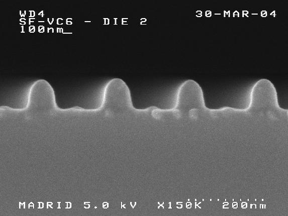
116 Figure 5.1 Sub-100 nm posts printed on gallium arsenide wafer. (top) after breakthrough etch (bottom) after transfer etch Figure 5.2 Sub-100 nm lines printed on gallium arsenide wafer. (top) after breakthrough etch (bottom) after transfer etch 105
117 5.1.2 Multi-Layer Templates The ability to pattern multiple layers in one imprint step capitalizes on the micromolding nature of the SFIL process. Optical methods are restricted to patterning one resist layer at a time. Aerial images can only be captured in one resist layer per exposure step. Imprint methods, however, face no such patterning constraints. Multitiered structures written in the template can be reproduced with imprint lithography. Applications for the printing of multi-layer templates include T-gate structures, optical waveguides, and so called dual damascene processes where contacts and wires for interconnect levels are printed two layers at a time. The ability to print multiple layers in one patterning step promises significant reductions in the total number manufacturing steps required to make a given device. When considered in the context of high volume manufacturing operations, such consolidation of steps can offer tremendous cost savings. Initial production of multi-tiered templates used negative optical and e-beam resist to add material to template. Standard resist and oxide deposition processes were employed along with e-beam exposure of hydrogen silsesquioxane (HSQ) to create raised lines on the template surface. 1 Figure 5.3 shows a dual level template and figure 5.4 shows three level imprints in E4 resist. 106


118 Figure 5.3 Two tiered template Figure 5.4 Three level images printed in E4 imprint resist Functional Materials The printing of functional materials represents another means of reducing the number of steps to manufacture a given device. Traditional photolithographic and imprint lithography processes deposit and pattern a sacrificial resist. After transferring the pattern in the resist to an underlayer, the resist is stripped from the substrate. The replacement of sacrificial imprint resists with functional materials, or materials that 107
119 function in the finished device, eliminates the need for etch transfer and resist strip steps. As was the case with the multi-layer templates presented in the previous step, this consolidation of manufacturing steps offers potential cost savings. The micromolding nature of the SFIL process makes the use of these materials possible. Although SFIL resist materials must meet a number of material requirements such as viscosity, vapor pressure, surface energy, and cohesive strength, they must meet relatively few material property requirements to meet patterning processes needs. Although optical lithography requires high sensitivity, high contrast, high transparency resists, imprint lithography demands only that resist materials meet minimal transparency requirements and polymerize in the presence of cationic or radial initiators. The number of materials suitable for use as imprint resists is thus potentially much larger than the number of materials suitable for use as photoresists. This wide assortment of potential imprintable materials offers some interesting possibilities for materials selection. Sol gel materials, for example, represent an extensively researched group of materials commonly used for dielectric or photonic applications. The ability to incorporate such materials into the SFIL process flow would open up a new set of extensively studied materials and processes for SFIL use. Figure 5.5 presents two monomers studied for this application. Tetraethyl orthosilicate, or TEOS, is a commonly used precursor for silicon dioxide films used as dielectrics. Substitution of an acrylate or methacrylate pendant group for one of the ethoxy group allows the incorporation of these materials into imprint resist formulations. 108
120 O O O Si O O O O O Si O O Figure 5.5 Methacrylate functionalized oxide precursor monomers (left) methacrylated tetraethyl orthosilicate (right) methacrylated tetramethyl orthosilicate. These materials may be photocured using traditional SFIL patterning techniques and then post processed to drive polymerizations to completion. For the materials shown, the SFIL exposure step initiates polymerization via the methacrylate functionality and subsequent heating initiates crosslinking as ethoxy groups are evolved and siliconoxygen-silicon crosslinks are formed. This two step process blends the low cost high resolution patterning capabilities of SFIL with a large set of extensively studied materials with potential applications as functional resists. Figure 5.6 shows SEM images of imprinted resist formulations based on these materials. Ongoing work in this area includes the development of post imprint thermal cure processes and the adaptation of low-k dielectric monomers for SFIL patterning use. 109


121 Figure 5.6 SFIL printed oxide precursors 5.2 CONCLUSIONS The development of the SFIL process has focused on proof of concept demonstrations of each process step followed by incremental improvements in materials and process capabilities. From initial resists printed on simple imprint equipment to highly refined resist formulations printed on complex step and repeat imprint tools, this work has always focused on the development a manufacturing process completely compatible with existing semiconductor manufacturing techniques. The development of materials, processes, and equipment capable of producing sub 100 nm features with high fidelity represents perhaps the greatest achievement of SFIL work at The University of Texas. Proof of concept demonstrations of each step of the process and further incremental improvements have generated a great deal of industrial interest in SFIL technology. Given the applied nature of SFIL process development, many of the key discoveries are directly related to resist materials. Perhaps no other materials have 110
122 received as much attention during the development process as the set of materials used as imprint resists. These materials must exhibit low viscosity for residual layer and throughput, low vapor pressure to avoid evaporation during dispense, high cohesive strength to print with high fidelity. For many applications, they must also exhibit enough etch resistance to serve as etch masks for pattern transfer. Transfer layer materials must exhibit acceptable adhesion to cured resist materials. In addition, they must not dissolve when exposed to resist monomer in the dispense step. Etch process work is highly empirical in nature, and each developed process must be carefully tailored to the specific materials and etch equipment available for the desired application. Breakthrough etch applications utilize oxygen and fluorocarbon etch gases, and transfer etch applications use oxygen or ammonia processes. Etch anisotropy can improved via process parameters that conducive for high mean free paths for active species in the plasma. Modeling provides a cost effective means of shortening the development cycle of new etch processes. 5.3 FUTURE WORK Opportunities for future work fall into two broad categories: development of new imprint materials and fundamental analysis of process steps. Resist material development could include new classes of functional materials, imprint resists with improved etch resistance, adhesion promoters for substrates, and materials to enhance template separation. Analysis of specific process steps could include fundamental mechanisms for 111
123 template-resist separation as well as an analysis of the contribution of specific resist components to overall mechanical properties Functional materials Recent work has demonstrated the use of methacrylate functionalized TEOS and similar molecules as imprint resist components. TEOS was selected for use in these studies because of its widespread use as an oxide precursor and its applications in sol-gel chemistry. Sol-gels in general represent a large set of extensively researched materials. If protocols for high fidelity imprinting and post processing of these methacrylated TEOS materials can be established, they provide a means of sampling numerous other sol-gel chemistries for SFIL applications. Sol-gel-SFIL hybrid functional resists could serve as precursors for optical and ceramic materials. The use of composite resist materials also represents an opportunity to expand the set of materials used in SFIL applications. The inclusion of secondary materials such as silicon nanoparticles, C 60 buckyballs, or carbon nanotubes in standard SFIL patterned resists could provide the means to augment cured resist properties with minimal changes to liquid resist composition. The ability to combine SFIL patterning capability with properties of these materials may facilitate use of these materials in new applications. For example, current methods of depositing carbon nanotubes on semiconductor substrates include individual placement by AFM tip or growing nanotubes from catalysts previously deposited on the substrate. Development of an SFIL patterning process to deliver these new materials could enable cost effective applications of their unique 112
124 properties. Silicon nanoparticles provide a second application for immediate work in this area. Patterning imprint resist material laden with silion nanoparticle quantum dots could both broaden the process window used to produce the nanoparticles and facilitate precision placement at low cost. Research into the effects of quantum dots on optical or photonic systems could be of particular interest Improved Etch Properties Current imprint resists have been optimized for dispense control and imprint fidelity. Many resist formulations, including the E4 resist discussed in this dissertation, bear a very close resemblance to polymethyl methacrylate (PMMA) a common electron beam resist known for relatively poor etch resistance. Incorporation of cyclic or phenyl groups into the resist structure could yield improved etch properties quickly. Transfer layer materials could also benefit from an examination of their etch properties. Anti-reflective coatings, such as DUV30J-11 (Brewer Science), have served as convenient yet functional transfer layer materials for SFIL development. Other materials such as hard baked photoresists may offer the same ease of coating and adhesive properties as well as improved etch resistance. Improved transfer layer etch resistance could expand the overall SFIL process window Adhesion Promoters Resist-to-substrate and resist-to-transfer layer adhesion promoters offer another area for research. Although spin coated transfer layers often meet adhesion requirements, 113
125 future applications, particularly those utilizing the direct imprinting of functional materials, may benefit from more knowledge regarding adhesion promoters. As SFIL applications spread to various functional materials and across various substrates, one can imagine a library of adhesion promoters capable of coupling particular resist formulations to particular substrate materials. Research in this area could be particularly useful to industrial SFIL users who often posses the capability to develop highly controlled manufacturing processes but have minimal expertise in fundamental materials research Resist mechanical properties To date, much work has been done to develop imprint resists with sufficient mechanical properties for high fidelity imprinting. Acrylate systems, in particular, have received a great deal of attention as SFIL technology matured and expectations for resist imprint fidelity have increased. As patterning technology improves and imprinted samples are scrutinized with ever increasing levels of detail, a thorough understanding of the effect of imprint resist structure on mechanical properties may facilitate more informed decision making in the resist formulation process. Although mechanical properties and their impact on pattern fidelity may be the most important resist material property, they are not the only resist material property that must be considered. Viscosity, vapor pressure, etch resistance, and numerous other properties must all be considered in conjunction with mechanical properties when developing new imprint resist formulations. A better understanding of the impact of specific resist components on 114
126 mechanical properties will facilitate more sophisticated decision making when faced with conflicting resist requirements. At best, polymer structure-property correlations are difficult to identify. Some simple guidelines such as correlations between crosslinker composition and imprint fidelity have been observed, but more such correlations would be valuable. For example, extent of polymerization and its impact on mechanical properties could be an important area of SFIL study over the coming years. Small differences in extent of conversion can result in large differences in molecular weight with corresponding changes in mechanical properties. As SFIL lithographers begin to understand the underpinnings of imprint resist mechanical properties, they can make better informed decisions when developing new resist materials Template release mechanisms Fundamental mechanisms for template-resist separation after exposure offer an opportunity to apply engineering analysis to improve the imprint process. Given that device yields will be one of the most important metrics in determining SFIL printing success, an investigation of the fundamental mechanisms of template separation and resist mechanical properties is warranted. Current thought is that the template delaminates from the cured resist via the crack propagation method described previously in this dissertation. Ongoing work in this area should yield valuable insight into the nature of the separation process. As researchers determine the physical and chemical mechanisms that govern template separation, they should be able to design imprint materials and processes that print with 115
127 the highest possible fidelity. Both this area of research and an investigation of resist mechanical properties offer numerous educational opportunities for university students to learn analytical and fundamental problem solving techniques. REFERENCES 1. Johnson, S.C., Resnick, D.J., Mancini, D.P., Nordquist, K.J., Dauksher, W.J., Gehoski, K., Baker, J.H, Dues, L., Hooper, A., Bailey, T.C., Sreenivasan, S.V., Ekerdt, J.G., Willson, C.G. Microelectronic Engineering, : p
128 Appendix A: Adhesion of Acrylic Elastomers to Patterned Glass Substrates in Step and Flash Imprint Lithography Abstract Frank Palmieri and Stephen Johnson Step and Flash Imprint Lithography (SFIL) is a low pressure, low temperature nanoimprint process designed for use in semiconductor manufacturing. A key step in the process involves the separation of a topographically patterned quartz template from a photocured elastomer. The separation of these two materials must occur completely at the quartz-polymer interface (adhesive failure) to form a viable print. This paper explores mode 1 and 2 separations given a common template geometry. The model applies both the ideal work of adhesion and plastic work of adhesion assuming adhesive failure occurs by crack propagation. The minimum separation force calculated was 0.25MPa for mode 1 failure. The minimum mode 2 separation force was 0.15MPa. Contrary to the model, mode 2 separation forces are expected to be greater than mode 1 forces. Finally a model showing the friction forces associated with shearing mode 2 surfaces once the mode 1 surfaces have undergone adhesive failure is presented. The total resistance to shearing a mode 2 interface was 1-10MPa over an interface separation of nm. The separation force can be decreased by introducing larger defects or cracks at the interface. The plastic work of adhesion may be decreased by using a more brittle polymer. 117
129 Introduction Step and Flash Imprint Lithography (SFIL) is a contact printing technique capable of producing nano-scale features. An important step in the SFIL process involves contacting a patterned quartz template with a photopolymerizable acrylate liquid and subsequently curing the liquid with ultraviolet radiation. Clean separation of the glass template from the cured polymer is essential to a successful print. It is the purpose of this project to explore the characteristics of this separation through an approximate model of adhesive energies, cohesive energies, and topographic geometry. A basic understanding of the behavior of this adhesive interface will allow the intelligent design and analysis of future photocured materials and templates to minimize defect rates in the imprint process. Figure 1 illustrates the SFIL process. Figure A.1 SFIL process 118
130 The separation step is dictated by the material properties of the etch barrier (to be discussed later) and the geometry of the sample. A commonly printed pattern for semiconductor processing is nested lines and spaces. The model template for this case is shown in figure 2. Nested lines and spaces with an aspect ratio of one result in equal amounts of surface in tension and in shear during a separation process. Mode 1 separation occurs at tensile interfaces, and Mode 2 separation occurs at shear interfaces. Glass Template Photocured Acrylic Elastomer Mode 1 Mode 2 Figure A.2: Region of interest with mode 1 and mode 2 surfaces 119
131 Methodology A vast amount of information on the subject of adhesion failure has be accumulated in the past several decades, however in many cases investigators were forced to use empirical methods. The most common theory on the mechanics of adhesion failure is based on the propagation of a defect in the adhesive interface. A crack at the interface will propagate under the condition where energy released by relaxing the strain is equal to or greater than the energy gained by creating new crack interface. This criterion results in c ( c U ) = 0 G eq(1) where G is the energy per unit length of the crack interface, U is the strain energy released by crack propagation, c is one half the length of an interior crack and σ F is the fracture stress. 1 The strain energy per unit volume is given by 2 σ U S = eq(2) 2E σ = σ F where σ is the applied force and E is the elastic modulus of the strained material. The strain energy released by relaxation around the crack is then given by U S multiplied by volume relaxed material per unit length of crack. 1 U πc σ = U Sπ c = eq(3) 2E The relaxed volume is assumed to be cylindrical with a characteristic radius equal to the crack length c. The energy released by crack extension is the driving force for crack propagation, and the energy stored by crack extension restricts crack propagation. 120
132 The energy stored upon crack propagation consists of the ideal work of adhesion, W a (due to the formation of two new surfaces) and the plastic work, W p (due to the permanent deformation of a region around the crack tip). This is given by G = W a + W p. Combining equations (1) and (3) we have c W c 2 2 πc σ ( + W ) = 0 a p 2E σ σ = F 2 πcσ F ( W + W ) = 0 a p E eq(4) eq(5) = ( W + W ) E πc 1 2 σ F a p eq(6) To understand how eq(6) dictates adhesive failure in the SFIL process, it must be applied to a model system. A uniform interface under tensile load is the simplest case. Material 1 Material 2 Crack Figure A.3: Separation of an interface under normal tensile load 121
133 Assuming that material 1 is infinitely more stiff than material 2 that is E 1 >>E 2, all of the strain energy will be stored in material 2 as it deforms under the load. This system is analogous to the SFIL system where material 1 is the fused silica template and material 2 is the highly crosslinked elastomer. For a perfectly brittle solid, i.e. no plastic deformation, W p is zero and G = W a. For most real solids, W p is significant and is often several orders of magnitude greater than W a. That is, for real solids G ~ W p. Accepting that Wp>>Wa, it is important to note that W p is often be a function of W a. That is, plastic work often cannot be performed without ideal adhesion or W p (W a =0) = 0. Plastic work arises from the permanent deformation of a material about the crack tip. Because the material has yielded and cannot return to its original geometry, the plastic strain energy will be stored even after crack propagation. This stored energy increases the energy of the interface. 3 W p is not well understood nor easily obtained by theoretical arguments. Other factors that may influence G are polymer entanglement, electrostatic attraction and covalent bonding. These phenomena can result in a significant adhesive bond with no dependence on the ideal work of adhesion, W a. Research performed to characterize W p is largely empirical and results depend greatly on the material properties and the geometry of a system. For this reason, an empirical value for G must be applied to the SFIL adhesion. For the SFIL process Wp is minimized by highly crosslinking the etch barrier. High crosslink density is known to decrease ductility and should promote a brittle failure of the interface. Even with the etch barrier is as much as 50% crosslinking material by weight, W p still greatly exceeds W a. 122
134 For a brittle material G = 10 5 erg/cm 2. (3) G can also be obtained for thin films and from material properties by G = σ ε t eq(4) where σ y is the tensile strength, ε σf is the fracture strain and t is the film thickness. From y σf equation 4, G = 130erg/cm 2 for cyanoacrylate, a material similar to etch barrier. 1,2 The tremendous disparity between these numbers is not fully understood. The later value is very similar to the ideal work of adhesion measured for the SFIL interface, W a = 70erg/cm 2. 4 Crack length, c is another parameter of great debate. It is generally a safe assumption that defects will always be present at an adhesive interface. The intrinsic flaw size is said to be about 50µm. 3 For the SFIL interface, the defect size is not easily defined. SFIL templates are wetted by the etch barrier completely, leaving no gas bubbles at the interface. It is difficult to assume a crack could extend 50µm along the interface, crossing over 10 or hundreds of nanoscopic features. It is more reasonable to to assume defects are smaller than the printed features approximately 5 to 10 nm in size. These cracks are extremely small and should result in large separation forces. A crack may also initiate at the template edge. Edge crack initiation may be more likely than other cases due to a phenomena effecting the etch barrier photocure process. Etch barrier is photocured by free radical polymerization. The free radical which cause polymerization of the etch barrier prepolymer are also reactive towards oxygen. The edges of the template are exposed to atmospheric oxygen, and due to Fickian diffusion, 10-50µm of etch barrier cannot be 123
 c (µm) W p (erg/cm 2 ) W a (erg/cm 2 ) σ F (Mpa) σ F (psi) 50 0.005 130 70 25.23 3659.5 50 10 130 70 0.56 81.8 50 50 130 70 0.25 36.6 50 0.005 100000 70 564.")
135 cured. The liquid ring of etch barrier prepolymer at the template edges may constitute a mechanical crack. Table 1 shows the results mode 1 fracture given potential surface energies and crack lengths. Table A.1: Mode 1 fracture stress E (Mpa) c (µm) W p (erg/cm 2 ) W a (erg/cm 2 ) σ F (Mpa) σ F (psi) Figure 4. A very similar evaluation may be performed for the mode 2 separation shown in Crack Material 1 Material 2 Figure A.4: Mode 2 separation 124
Development of Imprint Materials for the Step and Flash Imprint Lithography Process
 Development of Imprint Materials for the Step and Flash Imprint Lithography Process Frank Xu a, Nick Stacey b, Michael Watts a, Van Truskett a, Ian McMackin a, Jin Choi a, Philip Schumaker a, Ecron Thompson
Step and Flash Imprint Lithography for sub-100nm Patterning
 Step and Flash Imprint Lithography for sub-100nm Patterning Matthew Colburn, Annette Grot, Marie Amistoso, Byung Jin Choi, Todd Bailey, John Ekerdt, S.V. Sreenivasan, James Hollenhorst, C. Grant Willson
Template fabrication schemes for step and flash imprint lithography
 Microelectronic Engineering 61 6 (00) 461 467 www.elsevier.com/ locate/ mee Template fabrication schemes for step and flash imprint lithography * E. Ainley, A. Talin, K. Gehoski, J.H. Baker, B.J. Choi,
Introduction to Nanoscience and Nanotechnology
 Introduction to Nanoscience and Nanotechnology ENS 463 2. Principles of Nano-Lithography by Alexander M. Zaitsev alexander.zaitsev@csi.cuny.edu Tel: 718 982 2812 Office 4N101b 1 Lithographic patterning
Introduction to Micro/Nano Fabrication Techniques. Date: 2015/05/22 Dr. Yi-Chung Tung. Fabrication of Nanomaterials
 Introduction to Micro/Nano Fabrication Techniques Date: 2015/05/22 Dr. Yi-Chung Tung Fabrication of Nanomaterials Top-Down Approach Begin with bulk materials that are reduced into nanoscale materials Ex:
UV15: For Fabrication of Polymer Optical Waveguides
 CASE STUDY UV15: For Fabrication of Polymer Optical Waveguides Master Bond Inc. 154 Hobart Street, Hackensack, NJ 07601 USA Phone +1.201.343.8983 Fax +1.201.343.2132 main@masterbond.com CASE STUDY UV15:
Fabrication and Layout
 ECEN454 Digital Integrated Circuit Design Fabrication and Layout ECEN 454 3.1 A Glimpse at MOS Device Polysilicon Aluminum ECEN 475 4.2 1 Material Classification Insulators Glass, diamond, silicon oxide
Photolithography I ( Part 2 )
") 1 Photolithography I ( Part 2 ) Chapter 13 : Semiconductor Manufacturing Technology by M. Quirk & J. Serda Bjørn-Ove Fimland, Department of Electronics and Telecommunication, Norwegian University of Science
1 Photolithography I ( Part 2 ) Chapter 13 : Semiconductor Manufacturing Technology by M. Quirk & J. Serda Bjørn-Ove Fimland, Department of Electronics and Telecommunication, Norwegian University of Science
Advanced Polymers And Resists For Nanoimprint Lithography
 Q U A L I T Y A S S U R A N C E MICROSYSTEMS & NANOSYSTEMS SPECIAL REPORT Advanced Polymers And Resists For Nanoimprint Lithography Numerous polymer systems specifically designed for nanoimprint lithography
Introduction to Lithography
 Introduction to Lithography G. D. Hutcheson, et al., Scientific American, 290, 76 (2004). Moore s Law Intel Co-Founder Gordon E. Moore Cramming More Components Onto Integrated Circuits Author: Gordon E.
PROCESS FLOW AN INSIGHT INTO CMOS FABRICATION PROCESS
 Contents: VI Sem ECE 06EC63: Analog and Mixed Mode VLSI Design PROCESS FLOW AN INSIGHT INTO CMOS FABRICATION PROCESS 1. Introduction 2. CMOS Fabrication 3. Simplified View of Fabrication Process 3.1 Alternative
Copyright. Christopher James Mackay
 Copyright by Christopher James Mackay 2002 Development of a Baseline Process for the Integration of Step and Flash Imprint Lithography into a MOSFET Fabrication Process by Christopher James Mackay, B.S.
Thermal Nanoimprinting Basics
 Thermal Nanoimprinting Basics Nanoimprinting is a way to replicate nanoscale features on one surface into another, like stamping copies are made by traditional fabrication techniques (optical/ebeam lith)
Supporting Information: Model Based Design of a Microfluidic. Mixer Driven by Induced Charge Electroosmosis
 Supporting Information: Model Based Design of a Microfluidic Mixer Driven by Induced Charge Electroosmosis Cindy K. Harnett, Yehya M. Senousy, Katherine A. Dunphy-Guzman #, Jeremy Templeton * and Michael
Major Fabrication Steps in MOS Process Flow
 Major Fabrication Steps in MOS Process Flow UV light Mask oxygen Silicon dioxide photoresist exposed photoresist oxide Silicon substrate Oxidation (Field oxide) Photoresist Coating Mask-Wafer Alignment
Photolithography Process Technology
 Contents Photolithography Process - Wafer Preparation - Photoresist Coating - Align & Expose - Photoresist Development Process Control CD Measurement Equipment Expose System & Wafer Track Consumables Chemicals
Preface Preface to First Edition
 Contents Foreword Preface Preface to First Edition xiii xv xix CHAPTER 1 MEMS: A Technology from Lilliput 1 The Promise of Technology 1 What Are MEMS or MST? 2 What Is Micromachining? 3 Applications and
Photolithography. Dong-Il Dan Cho. Seoul National University Nano/Micro Systems & Controls Laboratory
 Lecture 9: Photolithography School of Electrical l Engineering i and Computer Science, Seoul National University Nano/Micro Systems & Controls Laboratory Email: dicho@snu.ac.kr URL: http://nml.snu.ac.kr
Plasma for Underfill Process in Flip Chip Packaging
 Plasma for Underfill Process in Flip Chip Packaging Jack Zhao and James D. Getty Nordson MARCH 2470-A Bates Avenue Concord, California 94520-1294 USA Published by Nordson MARCH www.nordsonmarch.com 2015
MCC. PMGI Resists NANO PMGI RESISTS OFFER RANGE OF PRODUCTS
 MCC PMGI RESISTS OFFER Sub.25µm lift-off processing Film thicknesses from 5µm Choice of resin blends for optimal undercut control High thermal stability Superior adhesion to Si, NiFe, GaAs, InP
Because of equipment availability, cost, and time, we will use aluminum as the top side conductor
 Because of equipment availability, cost, and time, we will use aluminum as the top side conductor Top Side Conductor vacuum deposition Aluminum sputter deposit in Argon plasma CVC 601-sputter deposition
Fabrication of sawtooth diffraction gratings using nanoimprint lithography
 Fabrication of sawtooth diffraction gratings using nanoimprint lithography Chih-Hao Chang, a) R. K. Heilmann, R. C. Fleming, J. Carter, E. Murphy, and M. L. Schattenburg Massachusetts Institute of Technology,
EE 527 MICROFABRICATION. Lecture 15 Tai-Chang Chen University of Washington EE-527 M4 MASK SET: NPN BJT. C (sub) A E = 40 µm x 40 µm
 A E = 40 µm x 40 µm") EE 527 MICROFABRICATION Lecture 15 Tai-Chang Chen University of Washington EE-527 M4 MASK SET: NPN BJT C (sub) E B A E = 40 µm x 40 µm 1 EE-527 M4 MASK SET: MOS C-V TEST CAPACITORS W = 10 µm L = 10 µm
EE 527 MICROFABRICATION Lecture 15 Tai-Chang Chen University of Washington EE-527 M4 MASK SET: NPN BJT C (sub) E B A E = 40 µm x 40 µm 1 EE-527 M4 MASK SET: MOS C-V TEST CAPACITORS W = 10 µm L = 10 µm
Fabrication Technology, Part I
 EEL5225: Principles of MEMS Transducers (Fall 2003) Fabrication Technology, Part I Agenda: Oxidation, layer deposition (last lecture) Lithography Pattern Transfer (etching) Impurity Doping Reading: Senturia,
EE 5344 Introduction to MEMS. CHAPTER 3 Conventional Si Processing
 3. Conventional licon Processing Micromachining, Microfabrication. EE 5344 Introduction to MEMS CHAPTER 3 Conventional Processing Why silicon? Abundant, cheap, easy to process. licon planar Integrated
Fabrication Process. Crystal Growth Doping Deposition Patterning Lithography Oxidation Ion Implementation CONCORDIA VLSI DESIGN LAB
 Fabrication Process Crystal Growth Doping Deposition Patterning Lithography Oxidation Ion Implementation 1 Fabrication- CMOS Process Starting Material Preparation 1. Produce Metallurgical Grade Silicon
EECS130 Integrated Circuit Devices
 EECS130 Integrated Circuit Devices Professor Ali Javey 9/13/2007 Fabrication Technology Lecture 1 Silicon Device Fabrication Technology Over 10 15 transistors (or 100,000 for every person in the world)
Invited paper. Issues on nanoimprint lithography with a single-layer resist structure. Applied Physics A Materials Science & Processing
 Appl. Phys. A 81, 1331 1335 (2005) DOI: 10.1007/s00339-005-3313-2 g.y. jung 1 w. wu 1 s. ganapathiappan 1 d.a.a. ohlberg 1 m. saif islam 2 x. li 1 d.l. olynick 3 h. lee 4 y. chen 5 s.y. wang 1 w.m. tong
Photoresist Coat, Expose and Develop Laboratory Dr. Lynn Fuller
 ROCHESTER INSTITUTE OF TECHNOLOGY MICROELECTRONIC ENGINEERING Photoresist Coat, Expose and Develop Laboratory Dr. Lynn Fuller Webpage: http://www.rit.edu/lffeee 82 Lomb Memorial Drive Rochester, NY 14623-5604
Lecture 22: Integrated circuit fabrication
 Lecture 22: Integrated circuit fabrication Contents 1 Introduction 1 2 Layering 4 3 Patterning 7 4 Doping 8 4.1 Thermal diffusion......................... 10 4.2 Ion implantation.........................
 Page 1 of 9 High-volume full-wafer step-and-flash imprint lithography S-FIL is a unique method for printing sub-100nm geometries [1-3]. When high-resolution alignment is needed, the S-FIL process uses
Soft Lithography. Jin-Goo Park. Materials and Chemical Engineering Hanyang University, Ansan. Electronic Materials and Processing Lab.
 Hanyang University Soft Lithography Jin-Goo Park Materials and Chemical Engineering Hanyang University, Ansan Electronic Materials and Processing Lab. Introduction to Soft Lithography Research Micro- Electro-
Understanding. Brewer Science
 Understanding ARC Products General ARC Presentation: Slide #1 Overview Anti-reflective coating introduction Types of anti-reflective coating Advantages to anti-reflective coatings Advantages to bottom
Polymer-based Microfabrication
 Polymer-based Microfabrication PDMS SU-8 PMMA Hydrogel 1 Soft Lithography Developed by Whitesides, et. al A set of techniques for microfabrication based on the use of lithography, soft substrate materials
Czochralski Crystal Growth
 Czochralski Crystal Growth Crystal Pulling Crystal Ingots Shaping and Polishing 300 mm wafer 1 2 Advantage of larger diameter wafers Wafer area larger Chip area larger 3 4 Large-Diameter Wafer Handling
Nanoimprinting in Polymers and Applications in Cell Studies. Albert F. YEE Chemical Engineering & Materials Science UC Irvine
 Nanoimprinting in Polymers and Applications in Cell Studies Albert F. YEE Chemical Engineering & Materials Science UC Irvine Presentation outline Motivation Reversal imprinting Soft inkpad imprinting on
Dow Corning WL-5150 Photodefinable Spin-On Silicone
 Dow Corning WL-515 Photodefinable Spin-On Silicone Properties and Processing Procedures Introduction Dow Corning WL-515 is a silicone formulation which can be photopatterned and cured using standard microelectronics
Dr. Priyabrat Dash Office: BM-406, Mob: Webpage: MB: 205
 Email: dashp@nitrkl.ac.in Office: BM-406, Mob: 8895121141 Webpage: http://homepage.usask.ca/~prd822/ MB: 205 Nonmanufacturing In continuation from last class... 2 Top-Down methods Mechanical-energy methods
Fabrication Technology
 Fabrication Technology By B.G.Balagangadhar Department of Electronics and Communication Ghousia College of Engineering, Ramanagaram 1 OUTLINE Introduction Why Silicon The purity of Silicon Czochralski
Microelectronic Device Instructional Laboratory. Table of Contents
 Introduction Process Overview Microelectronic Device Instructional Laboratory Introduction Description Flowchart MOSFET Development Process Description Process Steps Cleaning Solvent Cleaning Photo Lithography
Chapter 3 Silicon Device Fabrication Technology
 Chapter 3 Silicon Device Fabrication Technology Over 10 15 transistors (or 100,000 for every person in the world) are manufactured every year. VLSI (Very Large Scale Integration) ULSI (Ultra Large Scale
PHYS 534 (Fall 2008) Process Integration OUTLINE. Examples of PROCESS FLOW SEQUENCES. >Surface-Micromachined Beam
 Process Integration OUTLINE. Examples of PROCESS FLOW SEQUENCES. >Surface-Micromachined Beam") PHYS 534 (Fall 2008) Process Integration Srikar Vengallatore, McGill University 1 OUTLINE Examples of PROCESS FLOW SEQUENCES >Semiconductor diode >Surface-Micromachined Beam Critical Issues in Process
PHYS 534 (Fall 2008) Process Integration Srikar Vengallatore, McGill University 1 OUTLINE Examples of PROCESS FLOW SEQUENCES >Semiconductor diode >Surface-Micromachined Beam Critical Issues in Process
EE40 Lec 22. IC Fabrication Technology. Prof. Nathan Cheung 11/19/2009
 Suggested Reading EE40 Lec 22 IC Fabrication Technology Prof. Nathan Cheung 11/19/2009 300mm Fab Tour http://www-03.ibm.com/technology/manufacturing/technology_tour_300mm_foundry.html Overview of IC Technology
VLSI INTRODUCTION P.VIDYA SAGAR ( ASSOCIATE PROFESSOR) Department of Electronics and Communication Engineering, VBIT
 Department of Electronics and Communication Engineering, VBIT") VLSI INTRODUCTION P.VIDYA SAGAR ( ASSOCIATE PROFESSOR) contents UNIT I INTRODUCTION: Introduction to IC Technology MOS, PMOS, NMOS, CMOS & BiCMOS technologies. BASIC ELECTRICAL PROPERTIES : Basic Electrical
VLSI INTRODUCTION P.VIDYA SAGAR ( ASSOCIATE PROFESSOR) contents UNIT I INTRODUCTION: Introduction to IC Technology MOS, PMOS, NMOS, CMOS & BiCMOS technologies. BASIC ELECTRICAL PROPERTIES : Basic Electrical
Nano-imprinting Lithography Technology І
 Nano-imprinting Lithography Technology І Agenda Limitation of photolithograph - Remind of photolithography technology - What is diffraction - Diffraction limit Concept of nano-imprinting lithography Basic
Advanced developer-soluble gap-fill materials and applications
 Advanced developer-soluble gap-fill materials and applications Runhui Huang, Dan Sullivan, Anwei Qin, Shannon Brown Brewer Science, Inc., 2401 Brewer Dr., Rolla, MO, USA, 65401 ABSTRACT For the via-first
EUV optics lifetime Radiation damage, contamination, and oxidation
 EUV optics lifetime Radiation damage, contamination, and oxidation M. van Kampen ASML Research 10-11-2016 Preamble Slide 2 ASML builds lithography scanners High-resolution photocopiers Copies mask pattern
IC/MEMS Fabrication - Outline. Fabrication
 IC/MEMS Fabrication - Outline Fabrication overview Materials Wafer fabrication The Cycle: Deposition Lithography Etching Fabrication IC Fabrication Deposition Spin Casting PVD physical vapor deposition
The Physical Structure (NMOS)
") The Physical Structure (NMOS) Al SiO2 Field Oxide Gate oxide S n+ Polysilicon Gate Al SiO2 SiO2 D n+ L channel P Substrate Field Oxide contact Metal (S) n+ (G) L W n+ (D) Poly 1 3D Perspective 2 3 Fabrication
The Physical Structure (NMOS) Al SiO2 Field Oxide Gate oxide S n+ Polysilicon Gate Al SiO2 SiO2 D n+ L channel P Substrate Field Oxide contact Metal (S) n+ (G) L W n+ (D) Poly 1 3D Perspective 2 3 Fabrication
Technical Data Sheet Technisches Datenblatt
 AZ ECI 3000 Photoresist Universal i-line/crossover Photoresist Series GENERAL INFORMATION AZ ECI 3000 photoresist series are a family of fast positive resists with high resolution capabilities (0.4 µm
Test Patterns for Chemical Mechanical Polish Characterization
 Dobek S: CMP Characterization 15th Annual Microelectronic Engineering Conference, 1997 Test Patterns for Chemical Mechanical Polish Characterization Stanley 3. Dobek Senior Microelectronic Engineering
Contact mechanics of a flexible imprinter for photocured nanoimprint lithography
 Tribology Letters, Vol. 9, No., May 2005 (0 2005) DO: 0.007~24900542656 Contact mechanics of a flexible imprinter for photocured nanoimprint lithography G.M. McClellanda,*, C.T. Rettnera, M.W. Harta, K.R.
In-Situ Monitoring of Pattern Filling in Nano-Imprint Lithography Using Surface Plasmon Resonance
 Copyright 2011 American Scientific Publishers All rights reserved Printed in the United States of America Journal of Nanoscience and Nanotechnology Vol. 11, 1 6, 2011 In-Situ Monitoring of Pattern Filling
Study of the resist deformation in nanoimprint lithography
 Study of the resist deformation in nanoimprint lithography Yoshihiko Hirai, a) Masaki Fujiwara, Takahiro Okuno, and Yoshio Tanaka Department of Mechanical System Engineering, Graduate School of Engineering,
Micro- and Nano-Technology... for Optics
 Micro- and Nano-Technology...... for Optics 3.2 Lithography U.D. Zeitner Fraunhofer Institut für Angewandte Optik und Feinmechanik Jena Electron Beam Column electron gun beam on/of control magnetic deflection
4. Thermal Oxidation. a) Equipment Atmospheric Furnace
 Equipment Atmospheric Furnace") 4. Thermal Oxidation a) Equipment Atmospheric Furnace Oxidation requires precise control of: temperature, T ambient gas, G time spent at any given T & G, t Vito Logiudice 34 4. Thermal Oxidation b) Mechanism
4. Thermal Oxidation a) Equipment Atmospheric Furnace Oxidation requires precise control of: temperature, T ambient gas, G time spent at any given T & G, t Vito Logiudice 34 4. Thermal Oxidation b) Mechanism
Lecture 1A: Manufacturing& Layout
 Introduction to CMOS VLSI Design Lecture 1A: Manufacturing& Layout David Harris Harvey Mudd College Spring 2004 Steven Levitan Fall 2008 1 The Manufacturing Process For a great tour through the IC manufacturing
Lithography Simulation of Sub-0.30 Micron Resist Features for Photomask Fabrication using I-line Optical Pattern Generators
 Lithography Simulation of Sub-0.30 Micron Resist Features for Photomask Fabrication using I-line Optical Pattern Generators Benjamen M. Rathsack 1, Cyrus E. Tabery 1, Cece Philbin 2 and C. Grant Willson
NIL defect performance toward High volume mass production
 NIL defect performance toward High volume mass production Masayuki Hatano a, Kei Kobayashi a, Hiroyuki Kashiwagi a, Hiroshi Tokue a, Takuya Kono a, Nakasugi Tetsuro a, Eun Hyuk Choi b, Wooyung Jung b a
Technology. Semiconductor Manufacturing. Hong Xiao INTRODUCTION TO SECOND EDITION SPIE PRESS
 INTRODUCTION TO Semiconductor Manufacturing Technology SECOND EDITION Hong Xiao TECHNISCHE INFORMATIONSBiBUOTHEK UNIVERSITATSBIBLIOTHEK HANNOVER SPIE PRESS Bellingham,Washington USA Contents Preface to
ARC XL Series. Broadband g-line & i-line Anti-Reflective Coatings
 ARC XL Series Broadband g-line & i-line Anti-Reflective Coatings Why Use a Brewer Science ARC? Resist Resist Substrate ARC Substrate Without Brewer ARC With Brewer ARC Lithography Reflective Problems In
Processing guidelines
 Processing guidelines mr-uvcur21 series UV-curable Polymer for UV-based Nanoimprint Lithography Characteristics mr-uvcur21 is a liquid UV-curable polymer system with low viscosity and high curing rate
EE 330 Lecture 9. IC Fabrication Technology Part 2
 EE 330 Lecture 9 IC Fabrication Technology Part 2 Quiz 8 A 2m silicon crystal is cut into wafers using a wire saw. If the wire diameter is 220um and the wafer thickness is 350um, how many wafers will this
Chapter 2 Manufacturing Process
 Digital Integrated Circuits A Design Perspective Chapter 2 Manufacturing Process 1 CMOS Process 2 CMOS Process (n-well) Both NMOS and PMOS must be built in the same silicon material. PMOS in n-well NMOS
EE 330 Lecture 9. IC Fabrication Technology Part II. -Oxidation -Epitaxy -Polysilicon -Planarization -Resistance and Capacitance in Interconnects
 EE 330 Lecture 9 IC Fabrication Technology Part II -Oxidation -Epitaxy -Polysilicon -Planarization -Resistance and Capacitance in Interconnects Review from Last Time IC Fabrication Technology Crystal Preparation
Process Flow in Cross Sections
 Process Flow in Cross Sections Process (simplified) 0. Clean wafer in nasty acids (HF, HNO 3, H 2 SO 4,...) --> wear gloves! 1. Grow 500 nm of SiO 2 (by putting the wafer in a furnace with O 2 2. Coat
CMOS Manufacturing process. Design rule set
 CMOS Manufacturing process Circuit design Set of optical masks Fabrication process Circuit designer Design rule set Process engineer All material: Chap. 2 of J. Rabaey, A. Chandrakasan, B. Nikolic, Digital
Polymer-based optical interconnects using nano-imprint lithography
 Polymer-based optical interconnects using nano-imprint lithography Arjen Boersma,Sjoukje Wiegersma Bert Jan Offrein, Jeroen Duis, Jos Delis, Markus Ortsiefer, Geert van Steenberge, MikkoKarppinen, Alfons
FABRICATION ENGINEERING MICRO- NANOSCALE ATTHE AND. Fourth Edition STEPHEN A. CAMPBELL. of Minnesota. University OXFORD UNIVERSITY PRESS
 AND FABRICATION ENGINEERING ATTHE MICRO- NANOSCALE Fourth Edition STEPHEN A. CAMPBELL University of Minnesota New York Oxford OXFORD UNIVERSITY PRESS CONTENTS Preface xiii prrt i OVERVIEW AND MATERIALS
Complexity of IC Metallization. Early 21 st Century IC Technology
 EECS 42 Introduction to Digital Electronics Lecture # 25 Microfabrication Handout of This Lecture. Today: how are Integrated Circuits made? Silicon wafers Oxide formation by growth or deposition Other
Today s Class. Materials for MEMS
 Lecture 2: VLSI-based Fabrication for MEMS: Fundamentals Prasanna S. Gandhi Assistant Professor, Department of Mechanical Engineering, Indian Institute of Technology, Bombay, Recap: Last Class What is
Metallization deposition and etching. Material mainly taken from Campbell, UCCS
 Metallization deposition and etching Material mainly taken from Campbell, UCCS Application Metallization is back-end processing Metals used are aluminum and copper Mainly involves deposition and etching,
Chapter 7 NANOIMPRINTED CIRCULAR GRATING DISTRIBUTED FEEDBACK DYE LASER
 Chapter 7 66 NANOIMPRINTED CIRCULAR GRATING DISTRIBUTED FEEDBACK DYE LASER 7.1 Introduction In recent years, polymer dye lasers have attracted much attention due to their low-cost processing, wide choice
micro resist technology
 Characteristics Processing guidelines Negative Tone Photoresist Series ma-n 1400 ma-n 1400 is a negative tone photoresist series designed for the use in microelectronics and microsystems. The resists are
Lecture 19 Microfabrication 4/1/03 Prof. Andy Neureuther
 EECS 40 Spring 2003 Lecture 19 Microfabrication 4/1/03 Prof. ndy Neureuther How are Integrated Circuits made? Silicon wafers Oxide formation by growth or deposition Other films Pattern transfer by lithography
CONTROLLING IMAGE PLACEMENT ERRORS DURING THE FABRICATION OF EUVL MASKS
 CONTROLLING IMAGE PLACEMENT ERRORS DURING THE FABRICATION OF EUVL MASKS Roxann L. Engelstad, Venkata Siva R. Battula, Pradeep Vukkadala, Andrew R. Mikkelson, Madhura Nataraju, and Kevin T. Turner Computational
Semiconductor Device Fabrication
 5 May 2003 Review Homework 6 Semiconductor Device Fabrication William Shockley, 1945 The network before the internet Bell Labs established a group to develop a semiconductor replacement for the vacuum
Microfabrication of Integrated Circuits
 Microfabrication of Integrated Circuits OUTLINE History Basic Processes Implant; Oxidation; Photolithography; Masks Layout and Process Flow Device Cross Section Evolution Lecture 38, 12/05/05 Reading This
More on VLSI Fabrication Technologies. Emanuele Baravelli
 More on VLSI Fabrication Technologies Emanuele Baravelli Some more details on: 1. VLSI meaning 2. p-si epitaxial layer 3. Lithography 4. Metallization 5. Process timings What does VLSI mean, by the way?
Chapter 3 CMOS processing technology
 Chapter 3 CMOS processing technology (How to make a CMOS?) Si + impurity acceptors(p-type) donors (n-type) p-type + n-type => pn junction (I-V) 3.1.1 (Wafer) Wafer = A disk of silicon (0.25 mm - 1 mm thick),
Module 13: Soft Lithography. Lecture 19: Soft Lithography 2
 Module 13: Soft Lithography Lecture 19: Soft Lithography 2 1 In the previous lecture we have introduced the concept of Soft Lithography and discussed three of the methods, which are Replica Molding, Micro
Chemical Vapor Deposition
 Chemical Vapor Deposition ESS4810 Lecture Fall 2010 Introduction Chemical vapor deposition (CVD) forms thin films on the surface of a substrate by thermal decomposition and/or reaction of gas compounds
A discussion of crystal growth, lithography, etching, doping, and device structures is presented in
 Chapter 5 PROCESSING OF DEVICES A discussion of crystal growth, lithography, etching, doping, and device structures is presented in the following overview gures. SEMICONDUCTOR DEVICE PROCESSING: AN OVERVIEW
Lect. 2: Basics of Si Technology
 Unit processes Thin Film Deposition Etching Ion Implantation Photolithography Chemical Mechanical Polishing 1. Thin Film Deposition Layer of materials ranging from fractions of nanometer to several micro-meters
Nanoscale Imaging, Material Removal and Deposition for Fabrication of Cutting-edge Semiconductor Devices
 Hitachi Review Vol. 65 (2016), No. 7 233 Featured Articles Nanoscale Imaging, Material Removal and Deposition for Fabrication of Cutting-edge Semiconductor Devices Ion-beam-based Photomask Defect Repair
Sub-5 nm Structures Process Development and Fabrication Over Large Areas
 A S Jugessur,, 2017, 1:1 SciFed Nanotech Research Letters Research Article Open Access Sub-5 nm Structures Process Development and Fabrication Over Large Areas * A S Jugessur * University of Iowa Microfabrication
Challenges and Future Directions of Laser Fuse Processing in Memory Repair
 Challenges and Future Directions of Laser Fuse Processing in Memory Repair Bo Gu, * T. Coughlin, B. Maxwell, J. Griffiths, J. Lee, J. Cordingley, S. Johnson, E. Karagiannis, J. Ehrmann GSI Lumonics, Inc.
Fabrication Technologies and Instruments. The available fabrication technologies and instruments for fabricating the sub-wavelength
 Chapter 3 Fabrication Technologies and Instruments 3.1 Introduction The available fabrication technologies and instruments for fabricating the sub-wavelength grating will be described in this chapter.
Lessons Learned from SEMATECH s Nanoimprint Program
 Accelerating the next technology revolution Lessons Learned from SEMATECH s Nanoimprint Program Matt Malloy Lloyd C. Litt Mac Mellish 10/19/11 Copyright 2010 SEMATECH, Inc. SEMATECH, and the SEMATECH logo
Basic&Laboratory& Materials&Science&and&Engineering& Micro&Electromechanical&Systems&& (MEMS)&
&") Basic&Laboratory& Materials&Science&and&Engineering& Micro&Electromechanical&Systems&& (MEMS)& M105& As of: 27.10.2011 1 Introduction... 2 2 Materials used in MEMS fabrication... 2 3 MEMS fabrication processes...
Basic&Laboratory& Materials&Science&and&Engineering& Micro&Electromechanical&Systems&& (MEMS)& M105& As of: 27.10.2011 1 Introduction... 2 2 Materials used in MEMS fabrication... 2 3 MEMS fabrication processes...
ECE 440 Lecture 27 : Equilibrium P-N Junctions I Class Outline:
 ECE 440 Lecture 27 : Equilibrium P-N Junctions I Class Outline: Fabrication of p-n junctions Contact Potential Things you should know when you leave Key Questions What are the necessary steps to fabricate
Three-dimensional SU-8 structures by reversal UV imprint
 Three-dimensional SU-8 structures by reversal UV imprint W. Hu, a B. Yang, C. Peng, and S. W. Pang b Solid State Electronics Laboratory, Department of Electrical Engineering and Computer Science, The University
THIN METALLIC LAYERS STRUCTURED BY E-BEAM LITHOGRAPHY. Miroslav HORÁČEK, Vladimír KOLAŘÍK, Michal URBÁNEK, František MATĚJKA, Milan MATĚJKA
 THIN METALLIC LAYERS STRUCTURED BY E-BEAM LITHOGRAPHY Miroslav HORÁČEK, Vladimír KOLAŘÍK, Michal URBÁNEK, František MATĚJKA, Milan MATĚJKA Ústav přístrojové techniky AV ČR, v. v. i., Královopolská 147,
Surface Micromachining
 Surface Micromachining Micro Actuators, Sensors, Systems Group University of Illinois at Urbana-Champaign Outline Definition of surface micromachining Most common surface micromachining materials - polysilicon
Platypus Gold Coated Substrates. Bringing Science to the Surface
 Platypus Gold Coated Substrates Bringing Science to the Surface Overview Gold Coated Substrates - Gold Coating Introduction - Glossary of Terms - Gold Coating Methods - Critical Features Platypus Gold
Vertically aligned Ni magnetic nanowires fabricated by diblock-copolymer-directed Al thin film anodization
 Vertically aligned Ni magnetic nanowires fabricated by diblock-copolymer-directed Al thin film anodization Researcher: Kunbae (Kevin) Noh, Graduate Student, MAE Dept. and CMRR Collaborators: Leon Chen,
Making of a Chip Illustrations
 Making of a Chip Illustrations 22nm 3D/Trigate Transistors Version April 2015 1 The illustrations on the following foils are low resolution images that visually support the explanations of the individual
High and Matched Refractive Index Liquid Adhesives for Optical Device Assembly
 As originally published in the SMTA Proceedings High and Matched Refractive Index Liquid Adhesives for Optical Device Assembly Taro Kenmochi Kyoritsu Chemical Chiyodaku, Tokyo, Japan Abstract There is
Illuminating Innovations
 Illuminating Innovations TM Silicone Solutions for LED Packaging Emir Debastiani Application Engineer Dow Corning Brazil Email: emir.debastiani@dowcorning.com Table of Contents Dow Corning Introduction
NanoSystemsEngineering: NanoNose Final Status, March 2011
 1 NanoSystemsEngineering: NanoNose Final Status, March 2011 The Nanonose project is based on four research projects (VCSELs, 3D nanolithography, coatings and system integration). Below, the major achievements