Opportuni)es to Move Up the Value Chain an OSAT Perspec)ve. Steve Ziolkowski ASE Group October 8, 2014
|
|
|
- Kristian Boone
- 6 years ago
- Views:
Transcription


1 Opportuni)es to Move Up the Value Chain an OSAT Perspec)ve Steve Ziolkowski ASE Group October 8, 2014
2 Overview Industry Dynamics and Opportunity ASE Overview Key Trends Growth Opportuni)es Enabling Factors Summary 2
3 Industry Dynamics Value chain consolida)on supply chain re- ver)caliza)on SoMware / service providers developing hardware plaoorms System OEMs & somware /service providers establishing IC design capability Crea)ng differen)ated plaoorm solu)ons through system integra)on and op)miza)on Moore s Law slowing Cost/transistor increasing for advanced process nodes High development, design and tooling cost Enabling alterna)ve integra)on paths to SoC Convergence accelera)on Mobile, wearable and IoT system products driving func)onal integra)on and miniaturiza)on Func)onal modules op)mized for performance, power and form factor Focus on energy, efficiency, connec)vity Reduced )me to market / revenue System BOM simplifica)on Ø Growing need for differen)ated packaging solu)ons to facilitate system integra)on, miniaturiza)on, op)miza)on and cost reduc)on 3
4 An emerging market System in Package A Differentiated Packaging Solution System in Package (SiP) will see exponen)al growth as systems integra)on, miniaturiza)on & power density trends con)nue. SiP Semiconductor: ~$330B OSAT: ~$26B Board Assembly: ~$700B Electronics: ~$1.8T Source: ASE estimates 4


5 System in Package/Module (SiP/SiM) A Differentiated Packaging Solution SiP/SiM is a package or module that contains a funchonal electronic system or sub- system that is integrated and miniaturized through IC assembly technologies Miniaturized Module Package Electronic System FuncHonality IC Assembly Technology 5

al")


6 SiP/SiM: Broad range of poten)al applica)ons Where Are The Key Growth Focus Areas? Touch Sensor Wireless Storage Power Management Camera Module RF Front End Lighting 6


7 ASE s Role in the Manufacturing Value Chain Vertical Integration Capabilities Module Board Assembly & Test (DMS) Final Test Material Assembly Wafer Bumping / Probing Foundry Engineering Test Integrated Circuit Design Services Offered by ASE Group 7


onal devices")


8 Leverage Capability to Enable OEM Drivers OEM System Integration Storage SSD in computing Various func)onal devices op)mized for SiP Processor FPGA/CPU for data center Display Camera in smart devices Power Management PMU in electric vehicle OSAT SiP Manufacturing: OEM s Enabler 8


9 Applica)ons Driving Growth Through 2018 Already Covering This Space Low Power, Tech Push, High Volume 39.0% 30.7% 18.2% 10.2% Utility Smartphone Ultramobile - Premium Clamshell Digital Set-Top Box - IP/Other $28b Solid State Drive 7.1% 4.4% -10.2% -13.2% ADAS $18b FTTx Infrastructure Ultramobile Utility Tablet Ultramobile - Basic Tablet $23b Basic Smartphone Premium Smartphone 13.8% Low End Server Most Categories < 10% CAGR & LCD TV < $10B revenues $50.6b Source: Gartner, June 2014 Semiconductor Forecast Database, Worldwide, 2Q14 Update Note: Y axis cut off at 0% for clarity, so some major markets like Desktop PCs do not appear in the chart as they have negative CAGR 9 9


10 Areas of Growth Poten)al for SiP Power Markets Power (Watt) 1G 100M 10M 1M 100k 10k 1k Motor drivers EV/HEV vehicles White goods hi fi audio Uninterruptible power supplies Power management for PCs Blade servers k 10k 100k 1M 10M 100M High Power Medium Power Power management for Wireless items Low Power Frequency (Hz) 10
11 Power Market Trends Power applica)ons span a huge space with differing requirements with respect to performance, cost, and size. The low power applica)on space is driving form factor reduc)on, func)onal integra)on etc. in high volumes. Higher power densi)es, faster switching speeds, and higher thermal requirements are pushing packaging technologies such as embedded die package (SiP) and Power Stack. These new packaging technology alterna)ves drive the need for new enabling technologies. - Interconnects - Limit performance losses - Package Construction - Better thermal management - Materials - Smaller form factor - Enable heterogeneous integration 11
12 Power Packaging Focus Areas for Growth Leveraging the need for SiP/SiM type packaging worldwide power semiconductor ~ $15bn : u Discrete ~ $11.5bn, module ~ $4bn. Discrete market commodi)zed / limited growth, but module market is projected to grow at 11% CAGR (transporta)on, renewable energy, EV/HEV & industrial motor drivers) IGBT is the major power module device type with ~$3.3Bn. Highest volumes in the 400v 1300V space. u IGBT market split by package type: ~20% Discrete, 8% IPM, and 72% Modules Yole (May 2013) 12


13 Power Packaging Focus Areas for Growth Leveraging the need for SiP/SiM type packaging.. Discrete Discrete power devices, usually packaged as traditional TO- 220, TO- 247 pkg Modules Modules contain single power circuity type such as MOSFET, IGBT module FOCUS Power Integrated Modules Intelligent Power Modules Power Stacks Power modules contain multiple power circuitry in single housing. Mostly IGBT Based Power modules that combine power transistor with control and protection circuity in single housing. Mostly IGBT Based Multiple power modules mounted on heat sink with driver and protective sensors and external components such as capacitor banks and interface terminals 13
14 Enablers for SiP in the Power Market Many possible combina)ons based on diverse market space: Business Model» Ownership and Support» Investment strategy across all areas below» Turnkey Levels and Scale Technology» Knowledge Base» IP» Design and Analysis CapabiliHes Collabora)on/Partnering» Customers» Supply Chain/CompeHtors» Industry ConsorHa / UniversiHes» Standards OrganizaHons Services Integra)on» VerHcal and Horizontal across Mfg, Bus, Tech, Support funchons 14
15 Business Models & Compe))ve Landscape n n n Ver)cal integra)on is prevalent for players in the power space. Discrete power semiconductor companies also expand their product poroolio to the module manufacturing There are also specialized power module makers Ø The opportunity is to complement exis)ng customers and non- ver)cally integrated players with technology and services that address power packaging trends while also enabling flex capacity to larger players. Vertical Integration Die + Module Modules + System Module Maker Systerm Maker source: Yole, 2013 Die Module System Mitsubishi, Fuji, ABB, Hitachi, Toshiba Fairchild, IR, IFX, STM, Vishay Danfoss, Electoviprymitel Semikron, Powerex, IXYS, Vincotech Schneider, Yaskawa, Siemens, Alstom 15

on - Flip chip")


16 Enabling Technologies for SiP/SiM Shielding - Board or package level - Compartmental Interconnec)on - Flip chip (MR & TCB) - Wire Bond Antenna - Package integrahon for 2.4G/5G/60GHz Molding - MUF - Exposed die SMT - Passives - Components - Connectors Thermal Management - Board or package level Compartmental Passives / IPD - Integrated Passive Devices Wafer Bumping / WLP - Leadfree / Cu Pillar - Bare die package Embedded Technology - Passive component - AcHve device Die / Pkg Stacking - Die thinning - Die interconnect - Die a]ach Mechanical Assy - Laser welding - Flex bending 16
17 ASE Technology Capability Mapping Coverage in the Power Space Power (Watt) 1G 100M 10M 1M 100k 10k 1k Integrated discretes (ASEWH-China) High Power Medium Power Low Power Module in ASENT IGBT MOSFET Embedded IC ASEKH SiC module GaN module k 10k 100k 1M 10M 100M Power management for wireless: DC/DC, LDO, PMIC = WLCSP, flip chip, Embedded IC in ASEKH, ASECL, ASEKR and ASEMY mid-power leadframe-based modules in ASEKR and ASEKH ASENT (metal die attach, Al ribbon bonding, ceramic DBC substrates, no molding, gel encapsulant) Other ASE sites (molded) Frequency (Hz) 17
18 Collabora)on Customer Road Map & Requirements Early Involvement Iden)fy Needs, Timing, and Poten)al Areas of Partnering u Business Requirements u Development achvihes u Infrastructure Requirements u Process/Equipment/Material CapabiliHes u QualificaHon Requirements Supply Chain Materials Equipment Piece Parts/BOM materials Assurance of Supply (Sourcing, Disaster Recovery, other risk mi)ga)on strategies) 18
19 Collabora)on Others Leverage involvement in Standards organiza)ons, Consor)a, University and 3 rd Party driven efforts Packaging Challenges Key Factors Current Solution Emerging Potential Breakthru Die Interconnect Die attache Substrate attach Resistivity Thermal Conductivity Lifetime Thermal cycling capability Themperature of operation Manufacturability Thermal performance Size / Volume reduction Al wire bonding Eutectic/Lead free Solder DBC + Substrate Al ribbon/ Cu wire bonding Ag u- powder sintering DBC to heat sink only Sintering Joint Nano powder sintering Micro- channel cooling source: Yole


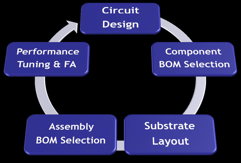

20 Collabora)on: SiP/SiM Design Flow Fine tune for performance improvement & BOM reduction Circuit Optimization & BOM reduction High Density SMT 20


on tooling")
vity KGD")


21 Collabora)on: SiP/SiM Test Services Test Strategy Consulta)on What tester to use? What/when/how to test? Test limits determina)on Test Fixture Design & Turnkey Socket, PCB Shielding Automa)on tooling Test Program Development Wireless connec)vity KGD wafer sort, final test Handler test controller Ramp up / Con)nuous Improvement Data analysis Yield Learning Test )me reduc)on Failure mode analysis Test Strategy Consulta)on Test Fixture Design & Turnkey Test Program Development Ramp up / Con)nuous Improvement 21

22 Leverage Enablers and Value Chain Enable electronic systems developers to achieve higher levels of functional integration and miniaturization Customer & Partners Test Assembly Supply Chain Substrate Consortia EMS/DMS 22
23 Changing Industry Landscape Value Chain Consolida)on is changing the industry: Innova)on, investment approaches as well as supply chain models. Specialized solu)ons for varying market spaces are driving complexity in terms of the number of approaches and choices needed to get an appropriate solu)on that sa)sfies both business and technical drivers. Need for Collabora)on in the form of standards, IP, and strategic partnerships (investment and sourcing) that are necessary for transi)ons to new markets. Opportuni)es in the space between tradi)onal OSATs and EMS providers will allow for further growth through leveraging capabili)es and knowledge from both ends. Having the right capabili)es, scale, flexibility and financial wherewithal to make it happen will be key. 23
24 Thank You 24
3D Wirebondless IGBT Module for High Power Applications Dr. Ziyang GAO Jun. 20, 2014
 3D Wirebondless IGBT Module for High Power Applications Dr. Ziyang GAO Jun. 20, 2014 1 1 Outline Background Information Technology Development Trend Technical Challenges ASTRI s Solutions Concluding Remarks
3D Package Technologies Review with Gap Analysis for Mobile Application Requirements. Apr 22, 2014 STATS ChipPAC Japan
 3D Package Technologies Review with Gap Analysis for Mobile Application Requirements Apr 22, 2014 STATS ChipPAC Japan T.Nishio Contents Package trends and roadmap update Advanced technology update Fine
System in Package: Identified Technology Needs from the 2004 inemi Roadmap
 System in Package: Identified Technology Needs from the 2004 inemi Roadmap James Mark Bird Amkor Technology Inc System in package (SiP) technology has grown significantly in the past several years. It
Semiconductor Packaging and Test A supply chain challenge
 Semiconductor Packaging and Test A supply chain challenge Jean-Marc Yannou Andrea Körtvelyessy ASE Group 16 th European Manufacturing Test Conference (EMTC) Session 3: Impact of new markets on test and
Roundtable 3DIC & TSV: Ready for HVM? European 3D TSV Summit
 Roundtable 3DIC & TSV: Ready for HVM? European 3D TSV Summit Infineon VTI Xilinx Synopsys Micron CEA LETI 2013 Yann Guillou Business Development Manager Lionel Cadix Market & Technology Analyst, Advanced
System-in-Package (SiP) on Wafer Level, Enabled by Fan-Out WLP (ewlb)
 on Wafer Level, Enabled by Fan-Out WLP (ewlb)") System-in-Package (SiP) on Wafer Level, Enabled by Fan-Out WLP (ewlb) Steffen Kröhnert, José Campos, Eoin O Toole NANIUM S.A., Vila do Conde, Portugal Outline Short Company Overview NANIUM Introduction
System-in-Package (SiP) on Wafer Level, Enabled by Fan-Out WLP (ewlb) Steffen Kröhnert, José Campos, Eoin O Toole NANIUM S.A., Vila do Conde, Portugal Outline Short Company Overview NANIUM Introduction
Close supply chain collaboration enables easy implementation of chip embedded power SiP
 Close supply chain collaboration enables easy implementation of chip embedded power SiP Gerald Weidinger, R&D Project Leader, AT&S AT & S Austria Technologie & Systemtechnik Aktiengesellschaft Fabriksgasse13
Challenges and Solutions for Cost Effective Next Generation Advanced Packaging. H.P. Wirtz, Ph.D. MiNaPAD Conference, Grenoble April 2012
 Challenges and Solutions for Cost Effective Next Generation Advanced Packaging H.P. Wirtz, Ph.D. MiNaPAD Conference, Grenoble April 2012 Outline Next Generation Package Requirements ewlb (Fan-Out Wafer
Semiconductor IC Packaging Technology Challenges: The Next Five Years
 SPAY025 May 2006 White Paper Mario A. Bolanos, Director Semiconductor Group Packaging Technology Development, Texas Instruments In the era of communications and entertainment, growth of consumer electronics
Thales vision & needs in advanced packaging for high end applications
 Thales vision & needs in advanced packaging for high end applications M. Brizoux, A. Lecavelier Thales Global Services / Group Industry Chemnitzer Seminar June 23 th -24 th, 2015 Fraunhofer ENAS - Packaging
Innovative Advanced Wafer Level Packaging with Smart Manufacturing Solutions YOON Seung Wook, Ph.D MBA
 Innovative Advanced Wafer Level Packaging with Smart Manufacturing Solutions YOON Seung Wook, Ph.D MBA Director, STATS ChipPAC Outline 1 2 3 Introduction of Smart Manufacturing & Wafer Level Packaging
Test Flow for Advanced Packages (2.5D/SLIM/3D)
") 1 Test Flow for Advanced Packages (2.5D/SLIM/3D) Gerard John Amkor Technology Inc. Gerard.John@amkor.com 2045 East Innovation Circle, Tempe, AZ 85284, USA Phone: (480) 821-5000 ADVANCED PACKAGE TEST FLOW
1 Test Flow for Advanced Packages (2.5D/SLIM/3D) Gerard John Amkor Technology Inc. Gerard.John@amkor.com 2045 East Innovation Circle, Tempe, AZ 85284, USA Phone: (480) 821-5000 ADVANCED PACKAGE TEST FLOW
Power Electronics Packaging Revolution Module without bond wires, solder and thermal paste
 SEMIKRON Pty Ltd 8/8 Garden Rd Clayton Melbourne 3168 VIC Australia Power Electronics Packaging Revolution Module without bond wires, solder and thermal paste For some years now, the elimination of bond
Panel Discussion: Advanced Packaging
 Dr. Steve Bezuk Senior Director IC Packaging Engineering Qualcomm Technologies, Inc. Panel Discussion: Advanced Packaging PAGE 1 Technical Challenges of Packaging (Mobile Focus) Materials Die materials
Packaging Technologies for SiC Power Modules
 Packaging Technologies for SiC Power Modules Masafumi Horio Yuji Iizuka Yoshinari Ikeda ABSTRACT Wide bandgap materials such as silicon carbide (SiC) and gallium nitride (GaN) are attracting attention
Prime Technology Inc.(PTI), Engineering Capability
, Engineering Capability") Technology, Knowhow, Services & Market Segments With large-scale resources and the broadest capital in the Electronics Manufacturing Services (EMS) industry, Prime Technology (PTI) provides services from
Technology, Knowhow, Services & Market Segments With large-scale resources and the broadest capital in the Electronics Manufacturing Services (EMS) industry, Prime Technology (PTI) provides services from
Power Electronics Packaging Solutions for Device Junction Temperature over 220 o C
 EPRC 12 Project Proposal Power Electronics Packaging Solutions for Device Junction Temperature over 220 o C 15 th August 2012 Page 1 Motivation Increased requirements of high power semiconductor device
Infineon FS820R08A6P2B HybridPACK Drive IGBT Module The newest HybridPACK Drive power module from Infineon with EDT2 IGBT technology
 Infineon FS820R08A6P2B HybridPACK Drive IGBT Module The newest HybridPACK Drive power module from Infineon with EDT2 IGBT technology With the push from various energy-saving applications, the overall IGBT
INVESTOR PRESENTATION
 INVESTOR PRESENTATION Rafi Amit, Chairman & CEO Moshe Eisenberg, CFO January 2017 Parts of almost all of today s latest devices have been made with the help of Camtek SAFE HARBOR The information presented
From Chip to System the demanding challenges for power semiconductor producers
 From Chip to System the demanding challenges for power semiconductor producers 29.07.2011 1 29.07.2011 2 In this talk we want to: Look at the market trends Tell you what demands they are placing on semiconductor
Business Renewal at Philips Semiconductors an overview of our journey
 Business Renewal at Philips Semiconductors an overview of our journey Frans van Houten CEO, Philips Semiconductors September 15, 2005 Agenda Philips Semiconductors: current performance Business Renewal:
Fan-out Wafer Level ewlb Technology as an Advanced System-in- Package Solution
 Fan-out Wafer Level ewlb Technology as an Advanced System-in- Package Solution by Jacinta Aman Lim and Vinayak Pandey, STATS ChipPAC, Inc. Aung Kyaw Oo, Andy Yong, STATS ChipPAC Pte. Ltd. Originally published
Investor presentation 24 April 2013
 Investor presentation 24 April 2013 2009 ASM Proprietary Information Safe Harbor Statements All matters discussed in this business and strategy update, except for any historical data, are forward-looking
3D-WLCSP Package Technology: Processing and Reliability Characterization
 3D-WLCSP Package Technology: Processing and Reliability Characterization, Paul N. Houston, Brian Lewis, Fei Xie, Ph.D., Zhaozhi Li, Ph.D.* ENGENT Inc. * Auburn University ENGENT, Inc. 2012 1 Outline Packaging
Graser User Conference Only
 2.5D/3D Design Solution Eric Chen & Scott Liu 31/Oct/2014 Roadmap data is provided for informational purposes only and does not represent a commitment to deliver any of the features or functionality discussed
LED Die Attach Selection Considerations
 LED Die Attach Selection Considerations Gyan Dutt & Ravi Bhatkal Alpha, An Alent plc Company Abstract Die attach material plays a key role in performance and reliability of mid, high and super-high power
Secondary Equipment view from an IDM Gareth BIGNELL
 Secondary Equipment view from an IDM Gareth BIGNELL Purchasing Director STMicroelectronics Agenda 2 What has changed for the Secondary Equipment & Applications (SEA) since activities started in 2012 How
Basic PCB Level Assembly Process Methodology for 3D Package-on-Package
 Basic PCB Level Assembly Process Methodology for 3D Package-on-Package Vern Solberg STC-Madison Madison, Wisconsin USA Abstract The motivation for developing higher density IC packaging continues to be
Making the most out of SiC. Alexander Streibel, Application Engineer
 Making the most out of SiC Alexander Streibel, Application Engineer WBG Power Conference December 5 th, Munich 2017 Content 1 Introduction to Danfoss Silicon Power 2 3 Danfoss Technologies DSP Activities
Forschung für die Elektroniksysteme von morgen
 Forschung für die Elektroniksysteme von morgen R. Aschenbrenner Outline Trends in Advanced Packaging Was ist Panel Level Packaging Embedding für Fan Out Embedding für LP Beispiele Trend on ICs and Packages
Challenges for Embedded Device Technologies for Package Level Integration
 Challenges for Embedded Device Technologies for Package Level Integration Kevin Cannon, Steve Riches Tribus-D Ltd Guangbin Dou, Andrew Holmes Imperial College London Embedded Die Technology IMAPS-UK/NMI
Cost effective 300mm Large Scale ewlb (embedded Wafer Level BGA) Technology
 Technology") Cost effective 300mm Large Scale ewlb (embedded Wafer Level BGA) Technology by Meenakshi Prashant, Seung Wook Yoon, Yaojian LIN and Pandi C. Marimuthu STATS ChipPAC Ltd. 5 Yishun Street 23, Singapore 768442
Cost effective 300mm Large Scale ewlb (embedded Wafer Level BGA) Technology by Meenakshi Prashant, Seung Wook Yoon, Yaojian LIN and Pandi C. Marimuthu STATS ChipPAC Ltd. 5 Yishun Street 23, Singapore 768442
Welcome to the KEMET Ceramic Capacitor Flex Crack Mitigation product training module. This module will review sources of stress in surface mount
 1 Welcome to the KEMET Ceramic Capacitor Flex Crack Mitigation product training module. This module will review sources of stress in surface mount multilayer ceramic capacitors, provide board layout recommendations,
Board Level Reliability Improvement in ewlb (Embedded Wafer Level BGA) Packages
 Packages") Board Level Reliability Improvement in ewlb (Embedded Wafer Level BGA) Packages by Seng Guan Chow, Yaojian Lin, Bernard Adams * and Seung Wook Yoon** STATS ChipPAC Ltd. 5 Yishun Street 23, Singapore 768442
Board Level Reliability Improvement in ewlb (Embedded Wafer Level BGA) Packages by Seng Guan Chow, Yaojian Lin, Bernard Adams * and Seung Wook Yoon** STATS ChipPAC Ltd. 5 Yishun Street 23, Singapore 768442
Introduction of CSC Pastes
 Introduction of CSC Pastes Smart Phones & Conductive Pastes Chip Varistors Chip Inductors LC Filters Flexible Printed Circuit Boards Electronic Molding Compounds ITO Electrodes PCB Through Holes Semiconductor
Alternative Approaches to 3-Dimensional Packaging and Interconnection
 Alternative Approaches to 3-Dimensional Packaging and Interconnection Joseph Fjelstad SiliconPipe, Inc. www.sipipe.com IC Packaging a Technology in Transition In the past, IC packaging has been considered
Chip Packaging for Wearables Choosing the Lowest Cost Package
 Chip Packaging for Wearables Choosing the Lowest Cost Package Alan Palesko alanp@savansys.com (512) 402-9943 www.savansys.com Slide - 1 Agenda Introduction Wearable Requirements Packaging Technologies
Failure Modes in Wire bonded and Flip Chip Packages
 Failure Modes in Wire bonded and Flip Chip Packages Mumtaz Y. Bora Peregrine Semiconductor San Diego, Ca. 92121 mbora@psemi.com Abstract The growth of portable and wireless products is driving the miniaturization
Industry Leading Provider of Outsourced Semiconductor Assembly, Test & Bumping Services
 Industry Leading Provider of Outsourced Semiconductor Assembly, Test & Bumping Services November, 217 Safe Harbor Notice This presentation contains certain forward-looking statements. These forward-looking
The 3D Silicon Leader
 The 3D Silicon Leader TSV technology embedding high density capacitors for advanced 3D packaging solutions IMAPS Device Packaging Conference 2014 Catherine Bunel 2014.03.12 Outline Introduction IPDiA s
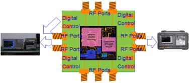
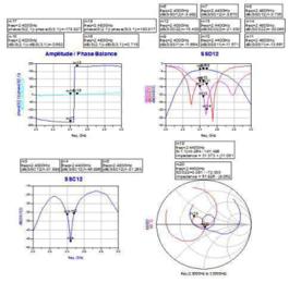
RF System in Packages using Integrated Passive Devices
 RF System in Packages using Integrated Passive Devices by Kai Liu, YongTaek Lee, HyunTai Kim, Gwang Kim, and Billy Ahn STATS ChipPAC 1711 W. Greentree Drive, Suite #117, Tempe, AZ 85284, USA Tel: 480-222-1722
Embedding Passive and Active Components: PCB Design and Fabrication Process Variations
 Embedding Passive and Active Components: PCB Design and Fabrication Process Variations Vern Solberg Solberg Technical Consulting Saratoga, California USA Abstract Embedding components within the PC board
Semiconductor Packaging and Assembly 2002 Review and Outlook
 Gartner Dataquest Alert Semiconductor Packaging and Assembly 2002 Review and Outlook During 2002, the industry continued slow growth in unit volumes after bottoming out in September 2001. After a hearty
Wire-Bond CABGA A New Near Die Size Packaging Innovation Yeonho Choi February 1, 2017
 Amkor Technology, Inc. White Paper Wire-Bond CABGA A New Near Die Size Packaging Innovation Yeonho Choi February 1, 2017 Abstract Expanding its ChipArray Ball Grid Array (CABGA) package form factor miniaturization
Electronic Costing & Technology Experts
 Electronic Costing & Technology Experts 21 rue la Nouë Bras de Fer 44200 Nantes France Phone : +33 (0) 240 180 916 email : info@systemplus.fr www.systemplus.fr May 2013 Version 1 Written by Romain Fraux
Design and Assembly Process Implementation of 3D Components
 IPC-7091 Design and Assembly Process Implementation of 3D Components Developed by the 3-D Electronic Packages Subcommittee (B-11) of the Packaged Electronic Components Committee (B-10) of IPC Users of
Non-Hermetic Packaging of RF Multi-Chip Modules
 Non-Hermetic Packaging of RF Multi-Chip Modules Matthew Gruber Lockheed Martin MST Moorestown, NJ 1 A Comment about this Presentation In accordance with ITAR restrictions, a few concessions had to be made
3D Integrated ewlb /FO-WLP Technology for PoP & SiP
 3D Integrated ewlb /FO-WLP Technology for PoP & SiP by Yaojian Lin, Chen Kang, Linda Chua, Won Kyung Choi and *Seung Wook Yoon STATS ChipPAC Pte Ltd. 5 Yishun Street 23, Singapore 768442 *STATS ChipPAC
Great Team Backend Foundry, Inc. ltd.com
 Great Team Backend Foundry, Inc. www.gtbf ltd.com 1 A leader of semiconductor packaging and tes?ng services, specialized in power management, small signal, discrete and control ICs packages. 2 Date of
Principles of Information Systems
 Principles of Information Systems Session 08 Systems Investigation and Analysis An Overview of Systems Development Today, users of informa0on systems are involved in their development Avoid costly failures
Silicon Interposers with Integrated Passive Devices: Ultra-Miniaturized Solution using 2.5D Packaging Platform
 Minapad 2014, May 21 22th, Grenoble; France Silicon Interposers with Integrated Passive Devices: Ultra-Miniaturized Solution using 2.5D Packaging Platform Stéphane Bellenger, Laëtitia Omnès, Jean-René
Long-term reliability of SiC devices. Power and Hybrid
 Long-term reliability of SiC devices Power and Hybrid Rob Coleman Business Development and Applications Manager TT electronics, Power and Hybrid Roger Tall Product Specialist Charcroft Electronics Ltd
Nondestructive Internal Inspection. The World s Leading Acoustic Micro Imaging Lab
 Nondestructive Internal Inspection The World s Leading Acoustic Micro Imaging Lab Unmatched Capabilities and Extensive Expertise At Your Service SonoLab, a division of Sonoscan, is the world s largest
Direct Liquid Cooling IGBT Module for Automotive Applications
 Direct Liquid Cooling IGBT Module for Automotive Applications Takahisa Hitachi Hiromichi Gohara Fumio Nagaune ABSTRACT A compact insulated gate bipolar transistor (IGBT) module with low thermal resistance
Mobile Device Passive Integration from Wafer Process
 Mobile Device Passive Integration from Wafer Process Kai Liu, YongTaek Lee, HyunTai Kim, and MaPhooPwint Hlaing STATS ChipPAC, Inc. 1711 West Greentree, Suite 117, Tempe, Arizona 85284, USA Tel: 48-222-17
2017 Annual Results Announcement. March 1, 2018
 2017 Annual Results Announcement March 1, 2018 Disclaimer The information contained in this presentation is provided for informational purpose only, and should not be relied upon for the purpose of making
IME Technical Proposal. High Density FOWLP for Mobile Applications. 22 April High Density FOWLP Consortium Forum
 IME Technical Proposal High Density FOWLP for Mobile Applications 22 April 2014 Packaging driver for portable / mobile applications Key drivers/needs Smaller form-factor lower profile, substrate-less Higher
Innovative Integration Solutions for SiP Packages Using Fan-Out Wafer Level ewlb Technology
 Innovative Integration Solutions for SiP Packages Using Fan-Out Wafer Level ewlb Technology Jacinta Aman Lim, Vinayak Pandey* STATS ChipPAC Inc. 46429 Landing Parkway, Fremont, CA 94538, USA *STATS ChipPAC
NXP SCM-i.MX6 Quad High Density Fan-Out Wafer-Level System-in-Package
 NXP SCM-i.MX6 Quad High Density Fan-Out Wafer-Level System-in-Package The first ultra-small multi-die low power module with boot memory and power management integrated in a package-on-package compatible
Thin Wafers Bonding & Processing
 Thin Wafers Bonding & Processing A market perspective 2012 Why New Handling Technologies Consumer electronics is today a big driver for smaller, higher performing & lower cost device configurations. These
PCTB PC-LAB. Power Cycling Testbench for Power Electronic Modules. Power Cycling Test Laboratory
 PCTB Power Cycling Testbench for Power Electronic Modules PC-LAB Power Cycling Test Laboratory Technical Information PCTB power cycling test bench alpitronic has many years of experience in developing
Automotive Electronic Material Challenges. Anitha Sinkfield, Delphi
 Automotive Electronic Material Challenges Anitha Sinkfield, Delphi Automotive Electronic Material Challenges Project Update About inemi Project Participants Problem Statement Project Details Summary and
ALTERNATIVES TO SOLDER IN INTERCONNECT, PACKAGING, AND ASSEMBLY
 ALTERNATIVES TO SOLDER IN INTERCONNECT, PACKAGING, AND ASSEMBLY Herbert J. Neuhaus, Ph.D., and Charles E. Bauer, Ph.D. TechLead Corporation Portland, OR, USA herb.neuhaus@techleadcorp.com ABSTRACT Solder
Advanced Analytical Techniques for Semiconductor Assembly Materials and Processes. Jason Chou and Sze Pei Lim Indium Corporation
 Advanced Analytical Techniques for Semiconductor Assembly Materials and Processes Jason Chou and Sze Pei Lim Indium Corporation Agenda Company introduction Semiconductor assembly roadmap challenges Fine
Innovative MID Plating Solutions
 Innovative MID Plating Solutions High Reliability Wire Bond Technique for MIDs Jordan Kologe MacDermid Electronics Solutions jkologe@macdermid.com 1 MacDermid: Specialty Chemical Solutions Over 2000 Worldwide
Development of Next-Generation ewlb Packaging
 Development of Next-Generation ewlb Packaging by Seung Wook Yoon, Yaojian Lin, Pandi Chelvam Marimuthu and *Rajendra Pendse STATS ChipPAC Singapore *Fremont, California USA Ganesh V. P, Andreas Bahr and
Chinese American Semiconductor Professional Association (CASPA)
") Chinese American Semiconductor Professional Association (CASPA) 1159 Sonora Court, Suite 105, Sunnyvale, CA 94086 Tel: (408)940-4600; Email: office@caspa.com URL:http://www.caspa.com About Infineon Infineon
Chinese American Semiconductor Professional Association (CASPA) 1159 Sonora Court, Suite 105, Sunnyvale, CA 94086 Tel: (408)940-4600; Email: office@caspa.com URL:http://www.caspa.com About Infineon Infineon
TSV CHIP STACKING MEETS PRODUCTIVITY
 TSV CHIP STACKING MEETS PRODUCTIVITY EUROPEAN 3D TSV SUMMIT 22-23.1.2013 GRENOBLE HANNES KOSTNER DIRECTOR R&D BESI AUSTRIA OVERVIEW Flip Chip Packaging Evolution The Simple World of C4 New Flip Chip Demands
Cu$ng costs out of the supply chain: what works and what doesn't?
 Cu$ng costs out of the supply chain: what works and what doesn't? Charlie Wellins Senior Vice President, Supply Chain Solu7ons, CEVA Logis7cs October 18 2012 Trans- Pacific Mari7me Asia Conference Shenzhen,
Forecast of Used Equipment Market Based on Demand & Supply
 Forecast of Used Equipment Market Based on Demand & Supply 2013. 06. 05 Thomas LEE Ⅰ. Market Introduction 300 200 150 _ Wafer Demand by Devices Type and Used Equipment Targets 20 to 0.13 0.13 to 0.5 >
New Technology for High-Density LSI Mounting in Consumer Products
 New Technology for High-Density Mounting in Consumer Products V Hidehiko Kira V Akira Takashima V Yukio Ozaki (Manuscript received May 29, 2006) The ongoing trend toward downsizing and the growing sophistication
Low Temperature Co-fired Ceramics (LTCC) Multi-layer Module Boards
 Multi-layer Module Boards") Low Temperature Co-fired Ceramics () Multi-layer Module Boards Example: Automotive Application Example: Communication Application Murata's Low Temperature Co-fired Ceramics offer highly integrated substrates
Low Temperature Co-fired Ceramics () Multi-layer Module Boards Example: Automotive Application Example: Communication Application Murata's Low Temperature Co-fired Ceramics offer highly integrated substrates
White Paper Quality and Reliability Challenges for Package on Package. By Craig Hillman and Randy Kong
 White Paper Quality and Reliability Challenges for Package on Package By Craig Hillman and Randy Kong Background Semiconductor technology advances have been fulfilling Moore s law for many decades. However,
Development of System in Package
 Development of System in Package In recent years, there has been a demand to offer increasingly enhanced performance for a SiP that implements downsized and lower-profile chips at lower cost. This article
Best-Reliable Ambient Intelligent Nanosensor Systems by Heterogeneous Integration
 Best-Reliable Ambient Intelligent Nanosensor Systems by Heterogeneous Integration 3D Workshop ESREF 2012, Cagliari Italy Reinhard Pufall Infineon Technologies AG (page 1) Project Presentation Outline Project
Chips Face-up Panelization Approach For Fan-out Packaging
 Chips Face-up Panelization Approach For Fan-out Packaging Oct. 15, 2015 B. Rogers, D. Sanchez, C. Bishop, C. Sandstrom, C. Scanlan, TOlson T. REV A Background on FOWLP Fan-Out Wafer Level Packaging o Chips
"ewlb Technology: Advanced Semiconductor Packaging Solutions"
 "ewlb Technology: Advanced Semiconductor Packaging Solutions" by Sharma Gaurav@, S.W. Yoon, Yap Yok Mian, Shanmugam Karthik, Yaojian Lin, Pandi C. Marimuthu and Yeong J. Lee* STATS ChipPAC Ltd. 5 Yishun
Company Presentation
 Company Presentation Overview Facts, Vision and Mission Portfolio, Markets and Capabilities Smart Cosmos The Internet of Your Things Quality and Certifications 2 Key Facts Global RFID and IoT pacesetter,
T3Ster. Thermal Transient Tester General Overview.
 T3Ster Thermal Transient Tester General Overview M e c h a n i c a l a n a l y s i s Safeguarding Against Temperature Related Performance Problems The relationship between high temperature and poor performance
Samsung 3D TSV Stacked DDR4 DRAM
 Samsung 3D TSV Stacked DDR4 DRAM The First Memory product with Via-Middle TSV! 3D TSV technology is expected to reach $4.8B in revenues by 2019, mainly driven by 3D stacked DRAM and followed by 3D Logic/Memory
Innovative Substrate Technologies in the Era of IoTs
 Innovative Substrate Technologies in the Era of IoTs Dyi- Chung Hu 胡迪群 September 4, 2015 Unimicron Contents Introduction Substrate Technology - Evolution Substrate Technology - Revolution Glass substrate
NW INNOVATIVE TECHNOLOGIES
 NW INNOVATIVE TECHNOLOGIES nwinnovative.com 5295 NE Elam Young Pkwy, Suite 160 Hillsboro OR 97124 TERRITORIES SERVED Oregon Washington Idaho/Montana JULIE MOORE OWNER/DIRECTOR OF SALES julie@nwinnovative.com
RF Integrated Passive Devices: Reverse Engineering & Costing Overview
 RF Integrated Passive Devices: Reverse Engineering & Costing Overview Technology and cost review of nine RF IPD found on the market from different suppliers: Broadcom, IPDiA, Murata, Qorvo, Skyworks and
Infineon RASIC: RRN7740 & RTN GHz Radar Dies
 Infineon RASIC: RRN7740 & RTN7750 77GHz Radar Dies New Receiver & Transmitter components with a SiGe:C HBT technology from Infineon The new integrated Radar and Camera (RACam) 77GHz automotive radar from
3D & 2½D Test Challenges Getting to Known Good Die & Known Good Stack
 1 3D & 2½D Test Challenges Getting to Known Good Die & Known Good Stack Advantest Corporation 2 The final yield Any Multi-die Product Must Consider the Accumulated Yield Assume Test Can Provide 99% Die
IMPLEMENTATION OF A FULLY MOLDED FAN-OUT PACKAGING TECHNOLOGY
 IMPLEMENTATION OF A FULLY MOLDED FAN-OUT PACKAGING TECHNOLOGY B. Rogers, C. Scanlan, and T. Olson Deca Technologies, Inc. Tempe, AZ USA boyd.rogers@decatechnologies.com ABSTRACT Fan-Out Wafer-Level Packaging
Toyota Prius 4 PCU Power Modules
 Toyota Prius 4 PCU Power Modules Toyota Prius 4 PCU modules integrate IGBT and freewheeling diodes onto innovative double side cooling packaging for hybrid electric vehicles, allowing better thermal dissipation,
Aerosol Jet International User Group Meeting. Metallization and Functional Structures by Aerosol Jet deposition
 17.10.2012 1 2012 Aerosol Jet International User Group Meeting Metallization and Functional Structures by Aerosol Jet deposition Andreas Brose Institut für Mikro- und Sensorsysteme Lehrstuhl Mikrosystemtechnik
ams Multi-Spectral Sensor in the Apple iphone X
 ams Multi-Spectral Sensor in the Apple iphone X The most advanced multispectral 6-channel ambient light sensor, supplied and produced by ams for its biggest customer, Apple For the semiconductor industry,
Simulation of Embedded Components in PCB Environment and Verification of Board Reliability
 Simulation of Embedded Components in PCB Environment and Verification of Board Reliability J. Stahr, M. Morianz AT&S Leoben, Austria M. Brizoux, A. Grivon, W. Maia Thales Global Services Meudon-la-Forêt,
Infineon CooliR²Die Power Module
 Infineon CooliR²Die Power Module Infineon power module integrating an IGBT and diode into innovative packaging for electric vehicles. The innovative packaging shrinks the power module and enables better
Next Generation ewlb (embedded Wafer Level BGA) Packaging
 Packaging") Next Generation ewlb (embedded Wafer Level BGA) Packaging by Meenakshi Prashant, Kai Liu, Seung Wook Yoon Yonggang Jin, Xavier Baraton, S. W. Yoon*, Yaojian Lin*, Pandi C. Marimuthu*, V. P. Ganesh**, Thorsten
Next Generation ewlb (embedded Wafer Level BGA) Packaging by Meenakshi Prashant, Kai Liu, Seung Wook Yoon Yonggang Jin, Xavier Baraton, S. W. Yoon*, Yaojian Lin*, Pandi C. Marimuthu*, V. P. Ganesh**, Thorsten
YOUR Strategic TESTING ENGINEERING CONCEPT SMT FLIP CHIP PRODUCTION OPTO PACKAGING PROCESS DEVELOPMENT CHIP ON BOARD SUPPLY CHAIN MANAGEMENT
 YOUR Strategic TECHNOLOGY PARTNER Wafer Back-End OPTO PACKAGING PROCESS DEVELOPMENT CONCEPT FLIP CHIP PROTOTYping ENGINEERING TESTING SMT PRODUCTION CHIP ON BOARD SUPPLY CHAIN MANAGEMENT Next Level 0f
Beyond Hardware to Solutions
 Beyond Hardware to Solutions Paul Humphries President, High Reliability Solutions (HRS) Global megatrends shape the face of the world 1 Growing World Population By 2030, 8.3 billion people will live on
Hot Chips: Stacking Tutorial
 Hot Chips: Stacking Tutorial Choon Lee Technology HQ, Amkor Enabling a Microelectronic World Mobile Phone Technology Change Feature Phone Smartphone Smartphones as a Percentage of All Phones Source : The
Locations: Head Quarter : Nutley, NJ Chicago, IL & Ahmedabad, India
 Locations: Head Quarter : Nutley, NJ Chicago, IL & Ahmedabad, India www.pnconline.com Introduction Established in 1968 Head Quarters Nutley, NJ, USA Satellite locations: Chicago, China & India 100+ Employees
The 2005 ITRS Assembly and Packaging Roadmap
 The 05 ITRS Assembly and Packaging Roadmap About ITRS ITRS = International Technology Roadmap for Semiconductors Combined effort by semiconductor industries worldwide Major revisions in odd numbered years
Ultra Fine Pitch Bumping Using e-ni/au and Sn Lift-Off Processes
 Ultra Fine Pitch Bumping Using e-ni/au and Sn Lift-Off Processes Andrew Strandjord, Thorsten Teutsch, and Jing Li Pac Tech USA Packaging Technologies, Inc. Santa Clara, CA USA 95050 Thomas Oppert, and
ams Ambient Light Sensor (ALS) with WLCSP TSV Packaging
 with WLCSP TSV Packaging") ams Ambient Light Sensor (ALS) with WLCSP TSV Packaging World s Smallest Ambient Light Sensor for Wearable Applications ams has adopted through-silicon via (TSV) packaging technology for advanced light
ams Ambient Light Sensor (ALS) with WLCSP TSV Packaging World s Smallest Ambient Light Sensor for Wearable Applications ams has adopted through-silicon via (TSV) packaging technology for advanced light
Design for Flip-Chip and Chip-Size Package Technology
 Design for Flip-Chip and Chip-Size Package Technology Vern Solberg Solberg Technology Consulting Madison, Wisconsin Abstract As new generations of electronic products emerge they often surpass the capability