Nondestructive Internal Inspection. The World s Leading Acoustic Micro Imaging Lab
|
|
|
- Osborn Stevens
- 6 years ago
- Views:
Transcription


1 Nondestructive Internal Inspection The World s Leading Acoustic Micro Imaging Lab
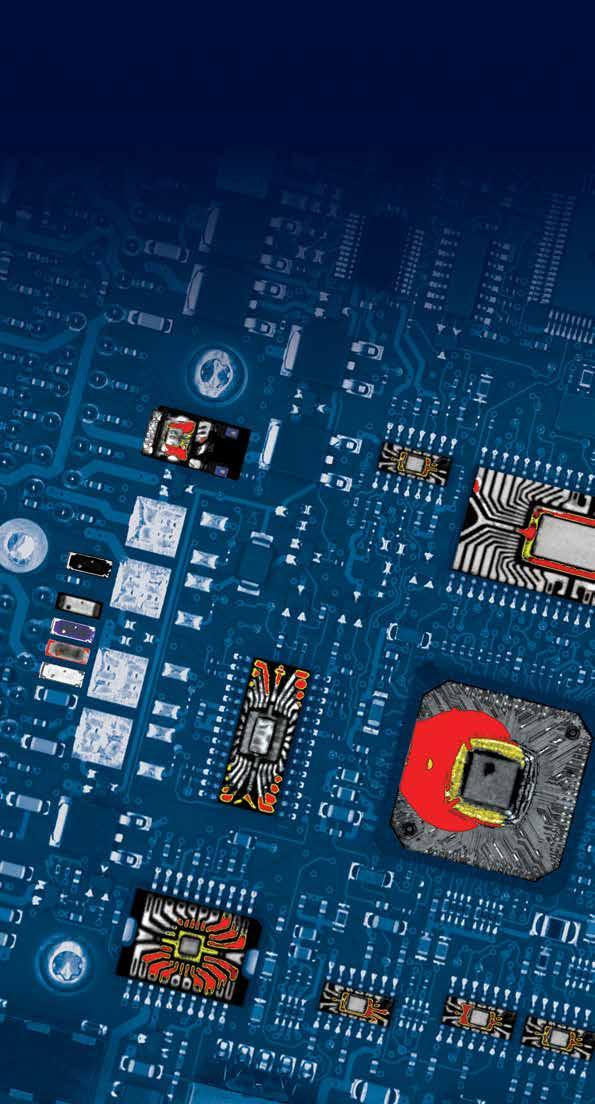
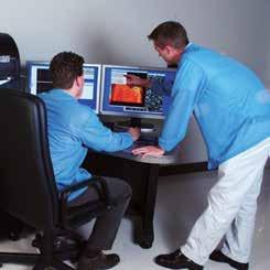
2 Unmatched Capabilities and Extensive Expertise At Your Service SonoLab, a division of Sonoscan, is the world s largest inspection service specializing in Acoustic Micro Imaging (AMI). Staffed by dedicated applications engineers, SonoLab delivers more experience in AMI applications than any other lab. Through SonoLab, you ll access the superior image quality and extraordinary data accuracy of Sonoscan C-SAM acoustic microscopes, while benefiting from the capabilities and careful analysis of the world s leading AMI experts. You ll receive detailed, illustrated reports as well as verbal consultation regarding your component s internal features, failure mechanism or accept/reject criteria. With Sonoscan-staffed lab locations worldwide and the full resources of Sonoscan, SonoLab brings the capability, flexibility and capacity to meet all your AMI requirements. Market Applications Acoustic Micro Imaging is relied upon for finding defects in a wide range of samples wherever the bonding between layers or the integrity of the materials themselves is of critical importance. A variety of market applications have benefited from SonoLab services: Microelectronics Plastic Encapsulated Microcircuits Ceramic Chip Capacitors Die Attach Chip Scale Packages (CSPs) Flip Chips Stacked Dies Ball Grid Arrays (BGAs/CBGAs) Tape Automated Bond (TAB) Hybrids, MCMs, SIPs Flex Circuits Printed Circuit Boards (PCBs) Smart Cards Bonded Wafers Thermo Electric Coolers (TECs) Power Modules Military, Aerospace and Automotive High-Rel Qualification Upscreening COTS Qualification Lead-free Devices Microelectromechanical Systems (MEMS) Bonded Wafers Fabrication Process Evaluation Zero Level Packaging Seal Level Packaging Packaging Sensors IMEMS MOEMS Lab-on-Chips BioChips Microarrays Composites Fiberglass Polymers Graphite Metal Matrix Hybrid Other Materials Glass Ceramics Plastics Adhesives Metals X-ray Targets Solar Energy Thin Film Polymer-Based Silicon Packaging, Seals Food Medical Pharma Other Hermetic Medical Materials Devices


3 SonoLab Services Need to analyze a lot of product quickly? Need independent verification? Need a flexible resource for acoustic microscopy? SonoLab has the capabilities to meet your needs. Services include: Component Qualification to Industry Standards SonoLab brings an unmatched combination of experience and technology in component qualification. Ensure your designs meet appropriate standards, such as IPC/JEDEC and various military and aerospace specifications, by putting SonoLab on your development team. Materials Characterization and Evaluation SonoLab will help you determine specific material properties or help you determine if a material has changed significantly compared to the qualified material. The unique nature of this inspection process reveals critical information on a component s construction while leaving the part undisturbed for further investigation. High-Capacity Screening and Lot Reclamation When you need parts quickly screened whether it s 1,000 pieces, 100,000 pieces or even more tap into SonoLab s unmatched capabilities and nearly limitless capacity. SonoLab gives you the ability to verify quality within a large sample size or separate good units from reliability risks as part of a lot reclamation initiative. Failure Analysis and Constructional Analysis SonoLab is the recognized standard for nondestructive analysis. SonoLab personnel will apply the most advanced techniques and technology and provide you with a detailed, illustrated report. You ll gain powerful insights regarding your component s internal features and failure mechanism and understand how you can prevent failures in the future. Inspection and Audit Services SonoLab delivers a comprehensive range of inspection services, including development, failure analysis and industry or military qualifications. In addition, SonoLab can be a valuable independent third-party resource for auditing the quality of purchased components. Custom Training If you currently own Sonoscan equipment, SonoLab s acoustic application engineers can create a customized program to meet your needs. Whether you have new personnel or new applications, wish to improve data and image interpretation skills, or want to learn advanced inspection methods, custom training will provide a lasting benefit. Industry Standards Sonoscan originated Acoustic Micro Imaging (AMI) and continues to work with various organizations to help develop qualification standards that improve component reliability. SonoLab inspection programs will meet all of your qualification needs. IPC/JEDEC J-STD-020 J-STD-035 J-STD-075 MEMS STANDARD SEMI MS MILITARY PERFORMANCE SPECIFICATION MIL-PRF-123 MIL-PRF MIL-PRF AEROSPACE (NASA & ESA) PEM-INST-001 (NASA/TP ) ESA/ESCC Basic Specification No MIL/AERO STANDARD GEIA-STD-0006 MILITARY STANDARD MIL-STD-883, METHOD 2030 MIL-STD-883, METHOD 2035 MIL-STD-1580B REQUIREMENT NASA S-311-P-829
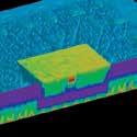
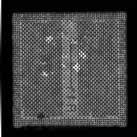
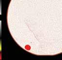
4 Inspection Examples & Results Plastic Encapsulated Microcircuit Hidden defects within an electronic package can often lead to catastrophic failure of the device. Critical delaminations (red and yellow areas) are revealed. Flip Chip Flip chip devices are routinely inspected for underfill, bump and silicon quality. The bright white areas observed in this flip chip image are voids in the underfill, which can lead to electrical failure. Ceramic Chip Capacitor Internal defects such as delaminations, cracks and voids within ceramic chip capacitors can lead to product failure. This inspection revealed delaminations and voids (bright white areas) within the active area. Bonded Wafer Evaluating bond quality in wafer pairs can uncover delaminated and voided regions that can lead to yield loss. Red areas indicate voids and delaminations detected between the wafers. Materials The mechanical strength of a composite can affect its performance. The bright white areas indicate voids and cracks stress points that can lead to mechanical failure, as happened here. MEMS Delaminations and voids can compromise the hermiticity of these devices. The regularly spaced red features are intentional air cavities that contain the actual MEMS devices. The remaining red areas are defects. State-of-the-Art Inspection at SonoLab You can depend on receiving the highest quality Acoustic Micro Imaging (AMI) when you entrust your parts to the professionals who invented the technology. Sonoscan s AMI is unmatched in its ability to find delaminations, voids, cracks and other hidden defects. Working exclusively with Sonoscan systems and technologies, our industryleading engineers use patented technology such as Virtual Rescanning Mode (VRM), an application that allows you to rescan your component even after it s been destroyed, to provide you with the most effective analysis services available.
5 Foil Seal In medical devices and pharmaceutical packaging, a seal is often used to keep the device or cavity contents sterile and contaminant-free. The bright white areas along the outer perimeter show several leak paths across the width of the seal. Thermo Electric Cooler The ability to actively transfer heat makes thermo electric coolers (TECs) useful devices in a variety of applications. The bright white features within the dark rectangles indicate voids at the direct bond copper (DBC) to ceramic substrate interface. Ball Grid Array This three-dimensional image also includes a crosssectional view through the center of this BGA. Depth information is gained from these views. The red feature near the center is from a void in the die attach. Power Module The ability to transfer heat from the die to the heat sink will often characterize how long a power device will function. The red areas are voids and delaminations between the die and heat sink. Thin Film Solar Cell The thin film cell structure is a multi-layered composite, where each layer must be interconnected and uniformly deposited and bonded. A missing interconnect can be seen in the lower left of the grid, along with delamination of the layers. Solar Concentrator The key reliability issue is the proper transfer of the excess solar thermal energy, requiring a consistent bond between the solar cell and the heat sink. The red areas indicate gaps in the cell-to-solder interface, which could cause loss of efficiency or failure of the structure. Stacked Die These images are from a BGA package containing a two-die stack. The first image indicates good bonding and silicon integrity at the first die. Inspection of the second die reveals a large diagonal crack within the silicon, noted by the red arrow. Additional smaller cracks are highlighted with yellow arrows.
6 SonoLab Locations Europe Silicon Valley Chicago Phoenix Shanghai SonoLab Silicon Valley 3350 Scott Blvd., Suite 5001 Santa Clara, CA Phone: Fax: SonoLab Southwest N. 87th St., Suite 217 Scottsdale, AZ Phone: Fax: SonoLab Central 2149 E. Pratt Blvd. Elk Grove Village, IL Phone: Fax: SonoLab Europe Unit 2, The Wincombe Business Centre Shaftesbury, Dorset SP7 9QJ England Phone: Fax: SonoLab Shanghai 2875 South Yang-Gao Rd. Building #1, Suite 1009 Pudong Shanghai PR China Phone: Fax: Sonoscan, Inc., Corporate Headquarters: 2149 E. Pratt Blvd., Elk Grove Village, IL T: F: Silicon Valley, CA Phoenix, AZ England Philippines Singapore Shanghai REV E
ECE414/514 Electronics Packaging Spring 2012 Lecture 2. Lecture Objectives
 ECE414/514 Electronics Packaging Lecture 2 James E. Morris Dept of Electrical & Computer Engineering Portland State University Lecture Objectives Introduce first-level interconnect technologies: wire-bond,
The Non-Destructive Test Method as A Simple Way to Evaluate The Quality of Metal Core PCBS for High Power Micro-Assemblies
 Indonesian Journal of Electrical Engineering and Computer Science Vol. 8, No. 2, November 2017, pp. 281 ~ 286 DOI: 10.11591/ijeecs.v8.i2.pp281-286 281 The Non-Destructive Test Method as A Simple Way to
Change Summary of MIL-PRF Revision K
 Throughout the document Add class Y. Add class Y non-hermetic for space application QML products to the MIL-PRF-38535., Class Y task group and Space community. Throughout the document Update Non-government
(13) PCB fabrication / (2) Focused assembly
 PCB fabrication / (2) Focused assembly") Company Fact Sheet TTM Technologies, Inc. is a world-wide leader in the manufacture of technologically advanced PCBs, backplane and sub-system assemblies. Our Global Presence / Local Knowledge approach
Company Fact Sheet TTM Technologies, Inc. is a world-wide leader in the manufacture of technologically advanced PCBs, backplane and sub-system assemblies. Our Global Presence / Local Knowledge approach
Ultrasound s sensitivity to material
 Acoustic Screening and Analysis of PEMs for Medical Applications Ultrasound can be used as a tool to test the reliability of medical electronics components. Tom Adams Ultrasound s sensitivity to material
Power electronics Building GaN HEMTs on 200 mm silicon
 BiHEMTs Simpler die boost battery life VCSELs Faster emitters eye chip-to-chip interconnects SiC wafers Scrutinizing surfaces with novel inspection tools Gas analysis Insider reveals how to succeed in
Selection and Application of Board Level Underfill Materials
 Selection and Application of Board Level Underfill Materials Developed by the Underfill Materials Design, Selection and Process Task Group (5-24f) of the Assembly and Joining Committee (5-20) of IPC Supersedes:
EP A2 (19) (11) EP A2 (12) EUROPEAN PATENT APPLICATION. (43) Date of publication: Bulletin 2006/23
 (11) EP A2 (12) EUROPEAN PATENT APPLICATION. (43) Date of publication: Bulletin 2006/23") (19) Europäisches Patentamt European Patent Office Office européen des brevets (12) EUROPEAN PATENT APPLICATION (11) EP 1 667 226 A2 (43) Date of publication: 07.06.06 Bulletin 06/23 (1) Int Cl.: H01L
(19) Europäisches Patentamt European Patent Office Office européen des brevets (12) EUROPEAN PATENT APPLICATION (11) EP 1 667 226 A2 (43) Date of publication: 07.06.06 Bulletin 06/23 (1) Int Cl.: H01L
The Development of a Novel Stacked Package: Package in Package
 The Development of a Novel Stacked Package: Package in Package Abstract Stacked die Chip Scale Packages (CSPs) or Fine-pitch BGAs (FBGAs) have been readily adopted and integrated in many handheld products,
High Reliability Optoelectronic Devices
 High Reliability Optoelectronic Devices Sensors and Specialist Components BI Technologies and OPTEK Technology Hi-Rel products, Hi-Rel service from OPTEK Technology TT Electronics OPTEK Technology solves
Abstract. Key words. I. Introduction
 Increased High-Temperature Reliability and Package Hardening of Commercial Integrated Circuits (Through Die Extraction, Electroless Nickel/Gold Pad Reconditioning, and Ceramic Re-Assembly) Erick M. Spory
Passive components : 5 years failure analysis feedback From all markets
 2 nd SPCD 12-14 October 2016 Passive components : 5 years failure analysis feedback From all markets Eric ZAIA (Material Engineer) Béatrice MOREAU (Passive components & PCB dpt. Manager) SUMMARY 1 Introduction
FLIP CHIP CHIP ON BOARD SMT ENGINEERING OPTO PACKAGING SUPPLY CHAIN MANAGEMENT TESTING YOUR INNOVATIVE TECHNOLOGY PARTNER PRODUCTION CONCEPT
 YOUR INNOVATIVE TECHNOLOGY PARTNER CHIP ON BOARD OPTO PACKAGING PROCESS DEVELOPMENT CONCEPT FLIP CHIP ENGINEERING TESTING PRODUCTION SMT SUPPLY CHAIN MANAGEMENT PROTOTYPES HIGH-PRECISION ASSEMBLY OF MICRO-
State of the Art,Inc. High Reliability Thick & Thin Film Resistive Products
 State of the Art,Inc. High Reliability Thick & Thin Film Resistive Products SOTA THE PROVEN SOURCE FOR THE WORLD S HIGHEST RELIABILITY RESISTIVE PRODUCTS Established in 1969, State of the Art, Inc. (SOTA)
YOUR Strategic TESTING ENGINEERING CONCEPT SMT FLIP CHIP PRODUCTION OPTO PACKAGING PROCESS DEVELOPMENT CHIP ON BOARD SUPPLY CHAIN MANAGEMENT
 YOUR Strategic TECHNOLOGY PARTNER Wafer Back-End OPTO PACKAGING PROCESS DEVELOPMENT CONCEPT FLIP CHIP PROTOTYping ENGINEERING TESTING SMT PRODUCTION CHIP ON BOARD SUPPLY CHAIN MANAGEMENT Next Level 0f
DIE SERVICES AND VALUE ADD
 545 VALUE ADD SERVICES DIE SERVICES AND VALUE ADD Teledyne Cougar offers a complete portfolio of Value Add and High Reliability services, including die upscreening, sorting, testing, packaging, binning,
Design and Assembly Process Implementation of 3D Components
 IPC-7091 Design and Assembly Process Implementation of 3D Components Developed by the 3-D Electronic Packages Subcommittee (B-11) of the Packaged Electronic Components Committee (B-10) of IPC Users of
Microelectronic Materials. Catalog
 Microelectronic Materials Catalog LORD partners with customers to leverage expertise in multiple chemistries and diverse applications to develop customized solutions. Design Without Compromise At LORD,
YOUR Strategic TESTING ENGINEERING CONCEPT SMT FLIP CHIP PRODUCTION OPTO PACKAGING PROCESS DEVELOPMENT CHIP ON BOARD SUPPLY CHAIN MANAGEMENT
 YOUR Strategic TECHNOLOGY PARTNER Wafer Back-End OPTO PACKAGING PROCESS DEVELOPMENT CONCEPT FLIP CHIP PROTOTYping ENGINEERING TESTING SMT PRODUCTION CHIP ON BOARD SUPPLY CHAIN MANAGEMENT Next Level 0f
Motorola PC603R Microprocessor
 Construction Analysis Motorola PC603R Microprocessor Report Number: SCA 9709-551 Global Semiconductor Industry the Serving Since 1964 17350 N. Hartford Drive Scottsdale, AZ 85255 Phone: 602-515-9780 Fax:
Fundamentals of Sealing and Encapsulation
 Fundamentals of Sealing and Encapsulation Sealing and Encapsulation Encapsulation and sealing are two of the major protecting functions of IC packaging. They are used to protect IC devices from adverse
Asia/Pacific Semiconductor Packaging and Assembly Facilities, 2002 (Executive Summary) Executive Summary
 Executive Summary") Asia/Pacific Semiconductor Packaging and Assembly Facilities, 2002 (Executive Summary) Executive Summary Publication Date: October 24, 2002 Author Philip Koh This document has been published to the following
Asia/Pacific Semiconductor Packaging and Assembly Facilities, 2002 (Executive Summary) Executive Summary Publication Date: October 24, 2002 Author Philip Koh This document has been published to the following
Microelectronic Materials CATALOG
 Microelectronic Materials CATALOG LORD partners with customers to leverage expertise in multiple chemistries and diverse applications to develop customized solutions. Design Without Compromise At LORD,
ENGINEERING PRACTICE (EP) STUDY
 STUDY") ENGINEERING PRACTICE (EP) STUDY TITLE: EP study on update of non-hermetic microcircuits class N (military, terrestrial and avionics application) and class Y (Space application) to MIL-PRF-38535. (Phase
ENGINEERING PRACTICE (EP) STUDY TITLE: EP study on update of non-hermetic microcircuits class N (military, terrestrial and avionics application) and class Y (Space application) to MIL-PRF-38535. (Phase
EPO-TEK Selector Guide
 Selector Guide www.epotek.com Electrically & Thermally Conductive Thermally Conductive/Electrically Insulating Optical/Fiber Optic Innovative Epoxy Adhesive Solutions for Over 45 Years Electrically & Thermally
Global Supplier. of Soldering. and Brazing. Preforms
 Global Supplier of Soldering and Brazing Preforms www.ametekmetals.c Responding quickly, precisely and efficiently to our customers needs Yes, we do. Our primary business at Coining is the fabrication
Flip Chip - Integrated In A Standard SMT Process
 Flip Chip - Integrated In A Standard SMT Process By Wilhelm Prinz von Hessen, Universal Instruments Corporation, Binghamton, NY This paper reviews the implementation of a flip chip product in a typical
General Introduction to Microstructure Technology p. 1 What is Microstructure Technology? p. 1 From Microstructure Technology to Microsystems
 General Introduction to Microstructure Technology p. 1 What is Microstructure Technology? p. 1 From Microstructure Technology to Microsystems Technology p. 9 The Parallels to Microelectronics p. 15 The
Material Set Comparison in Moisture Sensitivity Classification of Nonhermetic Organic Packages
 Material Set Comparison in Moisture Sensitivity Classification of Nonhermetic Organic Packages William R. Schildgen 3M Company Microinterconnect Systems Division 2020 Prairie Lane, P.O Box 2200 Eau Claire,
DAICO Industries. DAICO Industries, Inc E. 233rd. Street Carson, CA Tel: 310/ Fax: 310/
 DAICO Industries, Inc. 1070 E. 233rd. Street Carson, CA 90745 Tel: 310/507-3242 Fax: 310/507-5701 www.daico.com Founded in 1965, DAICO Industries, Inc. has been the leader in IF/RF Microwave Control Products
ELEC 6740 Electronics Manufacturing Chapter 5: Surface Mount Design Considerations
 ELEC 6740 Electronics Manufacturing Chapter 5: Surface Mount Design Considerations R. Wayne Johnson Alumni Professor 334-844 844-1880 johnson@eng.auburn. @eng.auburn.eduedu Outline System Design Issues
ELEC 6740 Electronics Manufacturing Chapter 5: Surface Mount Design Considerations
 ELEC 6740 Electronics Manufacturing Chapter 5: Surface Mount Design Considerations R. Wayne Johnson Alumni Professor 334-844-1880 johnson@eng.auburn. @eng.auburn.eduedu Outline System Design Issues Package
System in Package: Identified Technology Needs from the 2004 inemi Roadmap
 System in Package: Identified Technology Needs from the 2004 inemi Roadmap James Mark Bird Amkor Technology Inc System in package (SiP) technology has grown significantly in the past several years. It
Originally presented at NEPCON Southeast, Copyright 1999 AcousTech, Inc. INTRODUCTION
 A Case Study of PEMs Susceptible to Die Surface Delamination and Their Behavior During Thermal Excursions by Kerry D. Oren Senior Failure Analysis Engineer ITT Aerospace/Communications Originally presented
The Current State of the Art for Managing Electronic Component Obsolescence. Force Technologies Ltd
 The Current State of the Art for Managing Electronic Component Obsolescence 2014 Force Technologies Ltd Contents Introduction FPGA Remanufacturing & Emulation Reverse Engineering Die Recovery and repackaging
OUR SPECIALTY OUR SCOPE. We specialize in the design and manufacture of thick-film hybrid microcircuits and custom packagings.
 OUR SPECIALTY We specialize in the design and manufacture of thick-film hybrid microcircuits and custom packagings. OUR SCOPE We serve the global market, catering to the specific needs of a broad range
Assembly Reliability of TSOP/DFN PoP Stack Package
 As originally published in the IPC APEX EXPO Proceedings. Assembly Reliability of TSOP/DFN PoP Stack Package Reza Ghaffarian, Ph.D. Jet Propulsion Laboratory, California Institute of Technology Pasadena,
Assembly Challenges in Developing 3D IC Package with Ultra High Yield and High Reliability
 Assembly Challenges in Developing 3D IC Package with Ultra High Yield and High Reliability Raghunandan Chaware, Ganesh Hariharan, Jeff Lin, Inderjit Singh, Glenn O Rourke, Kenny Ng, S. Y. Pai Xilinx Inc.
Challenges of Fan-Out WLP and Solution Alternatives John Almiranez
 Challenges of Fan-Out WLP and Solution Alternatives John Almiranez Advanced Packaging Business Development Asia Introduction to Fan-Out WLP Introduction World of mobile gadgetry continues to rapidly evolve
Quality in Electronic Production has a Name: Viscom. System Overview
 Quality in Electronic Production has a Name: Viscom System Overview Successful along the whole line with Viscom Circuit board manufacturing Paste print Finish S3070 AFI-Scan S3054QS Paste print Thick film
Oki M A-60J 16Mbit DRAM (EDO)
") Construction Analysis Oki M5117805A-60J 16Mbit DRAM (EDO) Report Number: SCA 9707-545 Global Semiconductor Industry the Serving Since 1964 17350 N. Hartford Drive Scottsdale, AZ 85255 Phone: 602-515-9780
Construction Analysis Oki M5117805A-60J 16Mbit DRAM (EDO) Report Number: SCA 9707-545 Global Semiconductor Industry the Serving Since 1964 17350 N. Hartford Drive Scottsdale, AZ 85255 Phone: 602-515-9780
MIL-STD-883K w/change 3
 METHOD 5001 PARAMETER MEAN VALUE CONTROL 1. PURPOSE. The purpose of this method is to define a technique for assuring a conformance to a maximum or minimum mean of a parameter measured in any test method
IPC -7095C Design and Assembly Process Implementation For BGAs
 IPC -7095C Design and Assembly Process Implementation For BGAs 1 Overview With the introduction of BGA components, things had to change: New design New assembly process New repair process New inspection
SLIM TM, High Density Wafer Level Fan-out Package Development with Submicron RDL
 2017 IEEE 67th Electronic Components and Technology Conference SLIM TM, High Density Wafer Level Fan-out Package Development with Submicron RDL YoungRae Kim 1, JaeHun Bae 1, MinHwa Chang 1, AhRa Jo 1,
An Advanced Reliability Improvement and Failure Analysis Approach to Thermal Stress Issues in IC Packages
 An Advanced Reliability Improvement and Failure Analysis Approach to Thermal Stress Issues in IC Packages Michael Hertl 1, Diane Weidmann 1, and Alex Ngai 2 1 Insidix, 24 rue du Drac, F-38180 Grenoble/Seyssins,
Design Guideline for Electrical & Electronic Parts used in Satellite Applications to Support Class T. October 4, 2016
 Design Guideline for Electrical & Electronic Parts used in Satellite Applications to Support Class T October 4, 2016 1. SCOPE This document is intended as a guide to assist a piece part manufacturer with
Micron Semiconductor MT4LC16M4H9 64Mbit DRAM
 Construction Analysis Micron Semiconductor MT4LC16M4H9 64Mbit DRAM Report Number: SCA 9705-539 Global Semiconductor Industry the Serving Since 1964 15022 N. 75th Street Scottsdale, AZ 85260-2476 Phone:
Recent Advances in Die Attach Film
 Recent Advances in Die Attach Film Frederick Lo, Maurice Leblon, Richard Amigh, and Kevin Chung. AI Technology, Inc. 70 Washington Road, Princeton Junction, NJ 08550 www.aitechnology.com Abstract: The
IPC Qualification and Performance Specification for Organic Multichip Module (MCM-L) Mounting and Interconnecting Structures IPC-6015
 Mounting and Interconnecting Structures IPC-6015") ASSOCIATION CONNECTING ELECTRONICS INDUSTRIES Qualification and Performance Specification for Organic Multichip Module (MCM-L) Mounting and Interconnecting Structures February 1998 A standard developed
ASSOCIATION CONNECTING ELECTRONICS INDUSTRIES Qualification and Performance Specification for Organic Multichip Module (MCM-L) Mounting and Interconnecting Structures February 1998 A standard developed
Development and Characterization of 300mm Large Panel ewlb (embedded Wafer Level BGA)
") Development and Characterization of 300mm Large Panel ewlb (embedded Wafer Level BGA) Seung Wook Yoon, Yaojian Lin and Pandi C. Marimuthu STATS ChipPAC Ltd. 5 Yishun Street 23, Singapore 768442 E-mail
Development and Characterization of 300mm Large Panel ewlb (embedded Wafer Level BGA) Seung Wook Yoon, Yaojian Lin and Pandi C. Marimuthu STATS ChipPAC Ltd. 5 Yishun Street 23, Singapore 768442 E-mail
United Adhesives. Aerospace Automotives Computers Electronics Green Energy Semiconductors Telecommunications
 United Adhesives Aerospace Automotives Computers Electronics Green Energy Semiconductors Telecommunications Welcome to United Adhesives, Inc. United Adhesives Inc. formulates and manufactures special adhesives
Customizing Processes for Hermetic Assembly Of Devices Designed for Plastic Packages (1 of 3)
") Customizing Processes for Hermetic Assembly Of Devices Designed for Plastic Packages (1 of 3) Charlie C. Megia Golden Altos Corporation 402 South Hillview Drive, Milpitas, CA 95035 cmegia@goldenaltos.com
Customizing Processes for Hermetic Assembly Of Devices Designed for Plastic Packages (1 of 3) Charlie C. Megia Golden Altos Corporation 402 South Hillview Drive, Milpitas, CA 95035 cmegia@goldenaltos.com
Enhancement Mode GaN FETs and ICs Visual Characterization Guide
 Enhancement Mode GaN FETs and ICs Visual Characterization Guide EFFICIENT POWER CONVERSION Alana Nakata, Vice President, Product Engineering, Efficient Power Conversion Corporation A detailed description
Flexible Substrates for Smart Sensor Applications
 Flexible Substrates for Smart Sensor Applications A novel approach that delivers miniaturized, hermetic, biostable and highly reliable smart sensor modules. AUTHORS Dr. Eckardt Bihler, Dr. Marc Hauer,
10 Manor Parkway, Suite C Salem, New Hampshire
 Micro-Precision Technologies (MPT) is an independent manufacturer of hybrid integrated circuits, multichip modules, and high-precision thick film substrates for the military, medical, avionics, optoelectronics,
Quality & Reliability Standards for Electronic Energy Meters / Padrões de qualidade & confiabilidade para medidores eletrônicos de energia Sergio
 Quality & Reliability Standards for Electronic Energy Meters / Padrões de qualidade & confiabilidade para medidores eletrônicos de energia Sergio Abramoff Quality & Reliability Standards for Electronic
CGA TRENDS AND CAPABILITIES
 As originally published in the SMTA Proceedings. CGA TRENDS AND CAPABILITIES Marti McCurdy Silicon Turnkey Solutions Milpitas, CA, USA MMcCurdy@sts-usa.co Isabel de Sousa, Robert Martel and Alain Lessard
NEC 79VR5000 RISC Microprocessor
 Construction Analysis NEC 79VR5000 RISC Microprocessor Report Number: SCA 9711-567 Global Semiconductor Industry the Serving Since 1964 17350 N. Hartford Drive Scottsdale, AZ 85255 Phone: 602-515-9780
White Paper Opto-Electronics: The Secret to Success
 White Paper Opto-Electronics: The Secret to Success Opto-Electronic Vendor Selection Introduction Qualification of new technologies, new vendors, or new manufacturing locations is one of the most challenging
Silicon Wafer Processing PAKAGING AND TEST
 Silicon Wafer Processing PAKAGING AND TEST Parametrical test using test structures regularly distributed in the wafer Wafer die test marking defective dies dies separation die fixing (not marked as defective)
Accurate Predictions of Flip Chip BGA Warpage
 Accurate Predictions of Flip Chip BGA Warpage Yuan Li Altera Corporation 11 Innovation Dr, M/S 422 San Jose, CA 95134 ysli@altera.com, (48)544-758 Abstract Organic flip chip BGA has been quickly adopted
VJ TECHNOLOGIES TECHNOLOGY FOR GLOBAL MARKETS
 VJ TECHNOLOGIES TECHNOLOGY FOR GLOBAL MARKETS INSPECTION SYSTEMS & SERVICES X-Ray Solutions VJ Inspection Systems offers state-of-the-art x-ray inspection solutions for the most demanding imaging applications.
Effect of Die Bonding Condition for Die Attach Film Performance in 3D QFN Stacked Die.
 Effect of Die Bonding Condition for Die Attach Film Performance in 3D QFN Stacked Die. A. JALAR, M. F. ROSLE, M. A. A. HAMID. School of Applied Physics, Faculty of Science and Technology Universiti Kebangsaan
Change Summary of MIL-PRF Revision L December 06, Update/ clarification
 (Rev. L) 2.2.1 2.3 Added BME capacitor specification reference MIL-PRF-32535 Capacitors, BME Chip, Multiple Layers, Fixed, Ceramic Dielectric, Established Reliability and Non- Established Reliability,
Advanced Materials for Thermal Management of Electronic Packaging
 Xingcun Colin Tong Advanced Materials for Thermal Management of Electronic Packaging Sprin ger Contents 1 Thermal Management Fundamentals and Design Guides in Electronic Packaging 1 Rationale of Thermal
Statement of Work (SOW) inemi Packaging TIG SiP Module Moldability Project
 inemi Packaging TIG SiP Module Moldability Project") Statement of Work (SOW) inemi Packaging TIG SiP Module Moldability Project Version #1.0 Date: April 22, 2016 Project Leader: Billy Ahn, STATS ChipPAC Co-Project Leader: Anthony Yang, Moldex3D inemi Staff:
Statement of Work (SOW) inemi Packaging TIG SiP Module Moldability Project Version #1.0 Date: April 22, 2016 Project Leader: Billy Ahn, STATS ChipPAC Co-Project Leader: Anthony Yang, Moldex3D inemi Staff:
Analog Devices ADSP KS-160 SHARC Digital Signal Processor
 Construction Analysis Analog Devices ADSP-21062-KS-160 SHARC Digital Signal Processor Report Number: SCA 9712-575 Global Semiconductor Industry the Serving Since 1964 17350 N. Hartford Drive Scottsdale,
This procedure shall apply to all microcircuit elements and semiconductors as follows:
 1019-1618 V 2 OF 7 NTS A 1.0 PURPOSE: The purpose of this document is to define the supplier requirements of all procured microcircuit elements (Integrated Circuits) and semiconductor elements (diodes,
Close supply chain collaboration enables easy implementation of chip embedded power SiP
 Close supply chain collaboration enables easy implementation of chip embedded power SiP Gerald Weidinger, R&D Project Leader, AT&S AT & S Austria Technologie & Systemtechnik Aktiengesellschaft Fabriksgasse13
Thermal Management Catalog
 Management Catalog P-THERM Interface Materials Polymer Science, Inc. offers a complete thermal management product line. Our P-THERM Interface Materials are designed to efficiently and effectively aid in
Selector Guide. Providing the Connections for your Success. Automotive ele c tronics
 Providing the Connections for your Success Selector Guide Automotive ele c tronics Conductive Adhesives - Materials for Harsh Environment Protection - Underfill Encapsulants Electrically Conductive Adhesives
Chapter 4 Fabrication Process of Silicon Carrier and. Gold-Gold Thermocompression Bonding
 Chapter 4 Fabrication Process of Silicon Carrier and Gold-Gold Thermocompression Bonding 4.1 Introduction As mentioned in chapter 2, the MEMs carrier is designed to integrate the micro-machined inductor
BGA Package Underfilm for Autoplacement. Jan Danvir Tom Klosowiak
 BGA Package Underfilm for Autoplacement Jan Danvir Tom Klosowiak NIST-ATP Acknowledgment Project Brief Microelectronics Manufacturing Infrastructure (October 1998) Wafer-Scale Applied Reworkable Fluxing
Development of gold to gold interconnection flip chip bonding for chip on suspension assemblies
 Microelectronics Reliability 42 (2002) 381 389 www.elsevier.com/locate/microrel Development of gold to gold interconnection flip chip bonding for chip on suspension assemblies C.F. Luk a,1, Y.C. Chan b,
5. Packaging Technologies Trends
 5. Packaging Technologies Trends Electronic products and microsystems continue to find new applications in personal, healthcare, home, automotive, environmental and security systems. Advancements in packaging
Chips Face-up Panelization Approach For Fan-out Packaging
 Chips Face-up Panelization Approach For Fan-out Packaging Oct. 15, 2015 B. Rogers, D. Sanchez, C. Bishop, C. Sandstrom, C. Scanlan, TOlson T. REV A Background on FOWLP Fan-Out Wafer Level Packaging o Chips
PRESSURE SENSORS CHALLENGES IN DESIGN AND PRODUCTION DR. MATTHIAS PESCHKE
 CHALLENGES IN DESIGN AND PRODUCTION DR. MATTHIAS PESCHKE OUR COMPANY We are a leading provider of sensor technology 1991 foundation 150.1 million sales revenues in 2016 850 employees 3 markets 9 development
Bridging Supply Chain Gap for Exempt High-Reliability OEM s
 Bridging Supply Chain Gap for Exempt High-Reliability OEM s Hal Rotchadl hrotchadl@premiers2.com www.premiers2.com Premier Semiconductor Services Tempe, AZ RoHS exempt high reliability OEMs breathed a
S o l a r E n e r g y A d h e s i v e S o l u t i o n s
 S o l a r E n e r g y A d h e s i v e S o l u t i o n s www.adhesivesresearch.com I n s i g h t s Research designs, develops, and manufactures one-of-a-kind, customized products in pressure-sensitive adhesives,
JOINT INDUSTRY STANDARD
 JOINT INDUSTRY STANDARD AUGUST 1999 Semiconductor Design Standard for Flip Chip Applications ASSOCIATION CONNECTING ELECTRONICS INDUSTRIES Semiconductor Design Standard for Flip Chip Applications About
Failure Modes in Wire bonded and Flip Chip Packages
 Failure Modes in Wire bonded and Flip Chip Packages Mumtaz Y. Bora Peregrine Semiconductor San Diego, Ca. 92121 mbora@psemi.com Abstract The growth of portable and wireless products is driving the miniaturization
DISTRIBUTION LIST CHANGE RECORD
 DISTRIBUTION LIST In charge of the document: L. LE ROY- Quality Director Copy to: Responsibility P. MAURICE President P.E. BERTHET Marketing and Sales Director P. RIGOBERT Manufacturing Director N. FIANT
3DIC Integration with TSV Current Progress and Future Outlook
 3DIC Integration with TSV Current Progress and Future Outlook Shan Gao, Dim-Lee Kwong Institute of Microelectronics, A*STAR (Agency for Science, Technology and Research) Singapore 9 September, 2010 1 Overview
S/C Packaging Assembly Challenges Using Organic Substrate Technology
 S/C Packaging Assembly Challenges Using Organic Substrate Technology Presented by Bernd Appelt ASE Group Nov. 17, 2009 Overview The Packaging Challenge Chip Substrate Interactions Stiffeners for FC-BGA
Copyright 2009 Year IEEE. Reprinted from 2009 Electronic Components and Technology Conference. Such permission of the IEEE does not in any way imply
 Copyright 2009 Year IEEE. Reprinted from 2009 Electronic Components and Technology Conference. Such permission of the IEEE does not in any way imply IEEE endorsement of any of Institute of Microelectronics
STANDARD SPACE PRODUCTS PROGRAM
 STANDARD SPACE PRODUCTS PROGRAM For general information on Analog Devices Space Qualified products please visit the following address. http://www.analog.com/aerospace For technical inquiries on Aerospace
Standard for handling, packing, shipping and use of moisture/reflow sensitive surface mount devices
 This is a preview - click here to buy the full publication,(&3$6 Edition 1.0 2000-08 Standard for handling, packing, shipping and use of moisture/reflow sensitive surface mount devices 38%/,&/
Failure Analysis for ewlb-packages Strategy and Failure Mechanisms
 Company Logo Failure Analysis for ewlb-packages Strategy and Failure Mechanisms Florian Felux Infineon Technologies AG Neubiberg, Germany Purpose Demonstration of adaption and application of various analysis
YXLON Cougar EVO PLUS
 YXLON Cougar EVO PLUS The best small footprint X-ray inspection system for LABORATORY applications Technology with Passion Choose a custom-built EVO solution for premium inspection Why compromise? As technology
Power Electronics Packaging Solutions for Device Junction Temperature over 220 o C
 EPRC 12 Project Proposal Power Electronics Packaging Solutions for Device Junction Temperature over 220 o C 15 th August 2012 Page 1 Motivation Increased requirements of high power semiconductor device
FLIP-CHIP TECHNOLOGIES AND GLOBAL MARKETS
 FLIP-CHIP TECHNOLOGIES AND GLOBAL MARKETS SMC089B July 2016 Sinha G. Project Analyst ISBN: 1-62296-329-6 BCC Research 49 Walnut Park, Building 2 Wellesley, MA 02481 USA 866-285-7215 (toll-free within the
Which advantages can further automation bring?
 Carsten Busch, Segment Manager, Solar PV, 5th SMET Advanced PV Technology Conference, Session 2: Module manufacturing challenges Which advantages can further automation bring? ABB Group May 24, 2009 Slide
ATC ATC. Commercial Off-the-Shelf (COTS) Commercial Off The Shelf. High Reliability Certification Program. Applications:
 Commercial Off The Shelf. High Reliability Certification Program. Applications:") ATC High Reliability Program Commercial Off The Shelf ATC Commercial Off-the-Shelf (COTS) High Reliability Program HA HB HC HD A Cost Effective approach to qualifying standard products for enhanced reliability
ATC High Reliability Program Commercial Off The Shelf ATC Commercial Off-the-Shelf (COTS) High Reliability Program HA HB HC HD A Cost Effective approach to qualifying standard products for enhanced reliability
Copyright 2008 Year IEEE. Reprinted from IEEE ECTC May 2008, Florida USA.. This material is posted here with permission of the IEEE.
 Copyright 8 Year IEEE. Reprinted from IEEE ECTC 8. 7 - May 8, Florida USA.. This material is posted here with permission of the IEEE. Such permission of the IEEE does not in any way imply IEEE endorsement
Advanced packaging technologies for MEMS Gregor Woldt, Head of R&D Dr. Gregor Zwinge, Managing Director
 Advanced packaging technologies for MEMS Gregor Woldt, Head of R&D Dr. Gregor Zwinge, Managing Director Microelectronic Packaging Dresden GmbH A First Sensor Company MPD is an integral part of First Sensor
Electrical and Fluidic Microbumps and Interconnects for 3D-IC and Silicon Interposer
 Electrical and Fluidic Microbumps and Interconnects for 3D-IC and Silicon Interposer Li Zheng, Student Member, IEEE, and Muhannad S. Bakir, Senior Member, IEEE Georgia Institute of Technology Atlanta,
Molding materials performances experimental study for the 3D interposer scheme
 Minapad 2014, May 21 22th, Grenoble; France Molding materials performances experimental study for the 3D interposer scheme Y. Sinquin, A. Garnier, M. Argoud, A. Jouve, L. Baud, J. Dechamp, N. Allouti,
Worldwide IC Package Forecast (Executive Summary) Executive Summary
 Executive Summary") Worldwide IC Package Forecast (Executive Summary) Executive Summary Publication Date: 7 August 2003 Author Masao Kuniba This document has been published to the following Marketplace codes: SEMC-WW-EX-0275
Worldwide IC Package Forecast (Executive Summary) Executive Summary Publication Date: 7 August 2003 Author Masao Kuniba This document has been published to the following Marketplace codes: SEMC-WW-EX-0275