TSV CHIP STACKING MEETS PRODUCTIVITY
|
|
|
- Cornelius Hudson
- 6 years ago
- Views:
Transcription

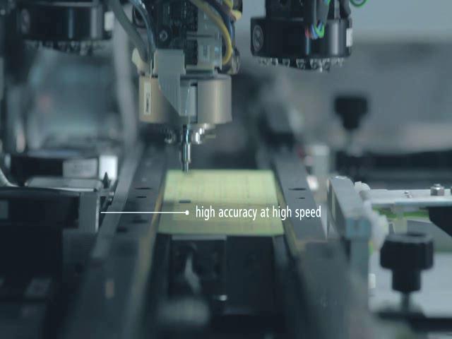
1 TSV CHIP STACKING MEETS PRODUCTIVITY EUROPEAN 3D TSV SUMMIT GRENOBLE HANNES KOSTNER DIRECTOR R&D BESI AUSTRIA
2 OVERVIEW Flip Chip Packaging Evolution The Simple World of C4 New Flip Chip Demands TCB Requirements for TSV Chip Stacking TCB Bonder Development Architectural considerations Innovation & Implementation Status and Outlook TCB Productivity Evaluations


3 FLIP CHIP PACKAGING EVOLUTION THE SIMPLE WORLD OF C4
4 FLIP CHIP PACKAGING EVOLUTION NEW FLIP CHIP DEMANDS MARKET DRIVERS integration density power consumption performance ultra low-k wide I/O low mechanical strength 3D & fine pitch gradient bonding copper pillar & thin die Thermo Compression Bonding Interconnect Technology
")


5 FLIP CHIP PACKAGING EVOLUTION NEW FLIP CHIP DEMANDS The world of TC Panel Singulated (Boat) Wafer Side by Side Strip Stacked Applications 2D TC 2.5D TSV 2.5 & 3D 3D TSV TC TC NCP Technologies TC CUF TC NCF TC MUF Upstream Dispensing Inert In-Situ Dispensing Fluxing C2S C2C C2W Multi Chip


6 FLIP CHIP PACKAGING EVOLUTION TCB REQUIREMENTS FOR TSV CHIP STACKING Through Silicon Via s Thin Die handling Cu-Pillars & CUF Bond Control I/O-Density & NCF Bondforce 250N Fine Pitch ± 2µm Placement Accuracy Cu-Pillars & Stacking 2µm@10mm Co-Planarity Insitu Soldering & Productivity Demands 200 C/s Heating & 100 C/s Cooling


7 FLIP CHIP PACKAGING EVOLUTION TCB REQUIREMENTS FOR TSV CHIP STACKING 3 TCB Core Capabilities are essential for yield! TCB Accuracy Core Capability #1 Co- Planarity Core Capability #2 Bond Control Core Capability #3
8 TCB BONDER DEVELOPMENT ARCHITECTURAL CONSIDERATIONS Rigid & Heavy Elastic & Lightweight Accuracy Co-Planarity Accurate Axis Appropriate Alignment system Thermal Drift Compensation Rigid System Accurate Axis Appropriate Alignment system Thermal Drift Compensation Mechatronic Co-planarity Control Bond Control z-stiffness Active z-position Control Productivity Limited by z-stiffness & Weight Fast Temp. Ramping Lightweight Construction Fast Temp. Ramping Flexibility per footprint Architectural Limits Comparable to C4 FC Bonder
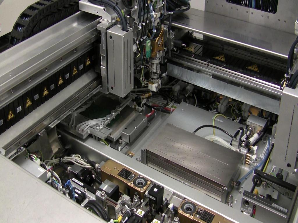
9 TCB BONDER DEVELOPMENT INNOVATION & IMPLEMENTATION CO-PLANARITY CONTROL Tilt due to elastic gantry deformation Kinematic Restraint System Mechatronics Solution with Coplanarity control


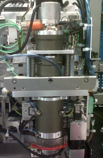
10 TCB BONDER DEVELOPMENT INNOVATION & IMPLEMENTATION 250N BONDHEAD
 Heater Tool Heater Tool Chip Chip")
11 TCB BONDER DEVELOPMENT INNOVATION & IMPLEMENTATION Active Gas cooling Cooling fluid (e.g. air) Heater Tool Heater Tool Chip Chip
![Temperatur [ c] TCB BONDER DEVELOPMENT INNOVATION](/docs-images/76/73804640/images/12-0.jpg "& IMPLEMENTATION Cooling ramp: -90 /sec 450 400")

12 Temperatur [ c] TCB BONDER DEVELOPMENT INNOVATION & IMPLEMENTATION Cooling ramp: -90 /sec Time [s] Temp P2 [ C] Temp P3 [ C] Temp P4 [ C] Temp P5 [ C]
13 PICK STATUS AND OUTLOOK TCB PRODUCTIVITY - ACTUAL Typical TC P&P cycle (TC process time: 4s) T [ C] max ramping: +100 C/s tool temperature 221 C 260 C max cooling: -50 C/s WAIT interval can be used for inspection 160 C 180 C 160 C Bond (TC process) MOVE REL MOVE WAIT MOVE ULC MOVE t [s] Phase 1: Bond (TC process) Phase 2: Move to rel. adjust Rel. Adjust Move to Pick Wait Phase 3: Pick Move to ULC Phase 4: ULC Move to Bond *) without inspections
14 PICK STATUS AND OUTLOOK TCB PRODUCTIVITY UPSIDE POTENTIAL Upside UPH: 2800 sprint UPH for machine T [ C] 160 C max ramping: +200 C/s 221 C 260 C tool temperature max cooling: -100 C/s 160 C 2.5 s cyle time / b. head based on +200/-100 C/s ramping Bond (TC process) MOVE REL MOVE MOVE ULC MOVE 1400 UPH / bond head t [s] Phase 1: Bond (TC process) Phase 2: Move to rel. adjust Rel. Adjust Move to Pick Phase 3: Pick Move to ULC Phase 4: ULC Move to Bond *) without inspections
15 STATUS AND OUTLOOK EVALUATIONS 1st TC-Bonder Buyoff was very successful with first time dual head/single pass assembly of Multi Layer TSV 50µ die thickness 2nd Evaluation is ongoing In total we talk to 27 companies. All are decided to utilize TCB technology sooner or later 12 OSATs 9 IDMs 2 Foundries 2 Fabless 2 Research Institutes 1 Material Supplier
16 SUMMARY
An Innovative High Throughput Thermal Compression Bonding Process
 An Innovative High Throughput Thermal Compression Bonding Process Li Ming 2 September 2015 Outline Introduction Throughput improved TCB Process Liquid Phase Contact (LPC) bonding Flux-LPC-TCB under inert
3D-IC Integration using D2C or D2W Alignment Schemes together with Local Oxide Reduction
 3D-IC Integration using D2C or D2W Alignment Schemes together with Local Oxide Reduction Gilbert Lecarpentier*, Jean-Stéphane Mottet* SET S.A.S. (Smart Equipment Technology), 131 Impasse Barteudet, 74490
3D Package Technologies Review with Gap Analysis for Mobile Application Requirements. Apr 22, 2014 STATS ChipPAC Japan
 3D Package Technologies Review with Gap Analysis for Mobile Application Requirements Apr 22, 2014 STATS ChipPAC Japan T.Nishio Contents Package trends and roadmap update Advanced technology update Fine
IME Technical Proposal. High Density FOWLP for Mobile Applications. 22 April High Density FOWLP Consortium Forum
 IME Technical Proposal High Density FOWLP for Mobile Applications 22 April 2014 Packaging driver for portable / mobile applications Key drivers/needs Smaller form-factor lower profile, substrate-less Higher
Material based challenge and study of 2.1, 2.5 and 3D integration
 1 Material based challenge and study of 2.1, 2.5 and 3D integration Toshihisa Nonaka Packaging Solution Center R&D Headquarters Hitachi Chemical Co., Ltd., Sep. 8, 2016 Hitachi Chemical Co., Ltd. 2010.
Fraunhofer IZM. All Silicon System Integration Dresden Scope. M. Juergen Wolf
 Fraunhofer IZM All Silicon System Integration Dresden Scope M. Juergen Wolf Fraunhofer IZM All Silicon System Integration - ASSID Dresden, Berlin, Germany Fraunhofer IZM Focus of Activities Materials,
Cost Analysis of Flip Chip Assembly Processes: Mass Reflow with Capillary Underfill and Thermocompression Bonding with Nonconductive Paste
 Cost Analysis of Flip Chip Assembly Processes: Mass Reflow with Capillary Underfill and Thermocompression Bonding with Nonconductive Paste Amy Palesko Lujan SavanSys Solutions LLC 10409 Peonia Court Austin,
S/C Packaging Assembly Challenges Using Organic Substrate Technology
 S/C Packaging Assembly Challenges Using Organic Substrate Technology Presented by Bernd Appelt ASE Group Nov. 17, 2009 Overview The Packaging Challenge Chip Substrate Interactions Stiffeners for FC-BGA
Cu Pillar Interconnect and Chip-Package-Interaction (CPI) for Advanced Cu Low K chip
 for Advanced Cu Low K chip") EPRC 12 Project Proposal Cu Pillar Interconnect and Chip-Package-Interaction (CPI) for Advanced Cu Low K chip 15 th Aug 2012 Page 1 Introduction: Motivation / Challenge Silicon device with ultra low k
EPRC 12 Project Proposal Cu Pillar Interconnect and Chip-Package-Interaction (CPI) for Advanced Cu Low K chip 15 th Aug 2012 Page 1 Introduction: Motivation / Challenge Silicon device with ultra low k
Challenges and Solutions for Cost Effective Next Generation Advanced Packaging. H.P. Wirtz, Ph.D. MiNaPAD Conference, Grenoble April 2012
 Challenges and Solutions for Cost Effective Next Generation Advanced Packaging H.P. Wirtz, Ph.D. MiNaPAD Conference, Grenoble April 2012 Outline Next Generation Package Requirements ewlb (Fan-Out Wafer
Henkel Adhesive Solutions for SiP Packaging. October 17-19, 2018 Shanghai, China
 Henkel Adhesive Solutions for SiP Packaging October 17-19, 2018 Shanghai, China Agenda 1 2 3 4 Overview: Henkel Adhesive Electronics Semiconductor Market Trends & SiP Drivers Henkel Adhesive Solutions
Fraunhofer IZM Bump Bonding and Electronic Packaging
 Fraunhofer IZM Bump Bonding and Electronic Packaging Fraunhofer Institute for Reliability and Microintegration (IZM) Gustav-Meyer-Allee 25 13355 Berlin Germany Dipl.-Ing. Thomas Fritzsch Contact: thomas.fritzsch@izm.fraunhofer.de
Henkel Enabling Materials for Semiconductor and Sensor Assembly. TechLOUNGE, 14 November 2017
 Henkel Enabling Materials for Semiconductor and Sensor Assembly TechLOUNGE, 14 November 2017 Content Brief HENKEL Introduction and ELECTRONICS Focus Areas Innovative Semiconductor and Sensor Assembly Solutions
Ultralow Residue Semiconductor Grade Fluxes for Copper Pillar Flip-Chip
 Ultralow Residue Semiconductor Grade Fluxes for Copper Pillar Flip-Chip SzePei Lim (Presenter), Jason Chou, Maria Durham, and Dr. Andy Mackie Indium Corporation 1 Outline of Presentation Roadmaps and challenges
SLIM TM, High Density Wafer Level Fan-out Package Development with Submicron RDL
 2017 IEEE 67th Electronic Components and Technology Conference SLIM TM, High Density Wafer Level Fan-out Package Development with Submicron RDL YoungRae Kim 1, JaeHun Bae 1, MinHwa Chang 1, AhRa Jo 1,
Die Bonder. Flip Chip Bonder Die Sorter
 Die Bonder Flip Chip Bonder Die Sorter T-6000-L/G Precision Die Attach Equipment with the most level of flexibility and customization T-6000-L T-8000-G T-6000-L/G Flexible High Precision Automatic Die
Next Gen Packaging & Integration Panel
 Next Gen Packaging & Integration Panel ECTC 2012 Daniel Tracy, Sr. Director Industry Research & Statistics SEMI May 29, 2012 Packaging Supply Chain Market Trends Material Needs and Opportunities Market
Advancements In Packaging Technology Driven By Global Market Return. M. G. Todd
 Advancements In Packaging Technology Driven By Global Market Return M. G. Todd Electronic Materials, Henkel Corporation, Irvine, California 92618, USA Recently, the focus of attention in the IC packaging
Challenges of Fan-Out WLP and Solution Alternatives John Almiranez
 Challenges of Fan-Out WLP and Solution Alternatives John Almiranez Advanced Packaging Business Development Asia Introduction to Fan-Out WLP Introduction World of mobile gadgetry continues to rapidly evolve
DEVELOPMENT DONE ON DEVICE BONDER TO ADDRESS 3D REQUIREMENTS IN A PRODUCTION ENVIRONMENT
 DEVELOPMEN DONE ON DEVICE BONDER O ADDRESS 3D REQUIREMENS IN A PRODUCION ENVIRONMEN Pascal Metzger, Ph.D., Joseph Macheda SE Corporation Saint-Jeoire, Haute-Savoie, France PMetzger@set-sas.fr Michael D.
Novel Materials and Activities for Next Generation Package. Hitachi Chemical., Co.Ltd. Packaging Solution Center Hiroaki Miyajima
 Novel Materials and Activities for Next Generation Package Hitachi Chemical., Co.Ltd. Packaging Solution Center Hiroaki Miyajima 1. Activities of Packaging Solution Center 2. Novel Materials for Next Gen.
Ultra Fine Pitch Bumping Using e-ni/au and Sn Lift-Off Processes
 Ultra Fine Pitch Bumping Using e-ni/au and Sn Lift-Off Processes Andrew Strandjord, Thorsten Teutsch, and Jing Li Pac Tech USA Packaging Technologies, Inc. Santa Clara, CA USA 95050 Thomas Oppert, and
A Flexible Vertical MEMs Probe Card Technology for Pre-Bump and ewlp Applications
 June 12 to 15, 2011 San Diego, CA A Flexible Vertical MEMs Probe Card Technology for Pre-Bump and ewlp Applications Mike Slessor Rick Marshall (MicroProbe, Inc.) Vertical MEMS for Pre-Bump Probe Introduction:
3D & 2½D Test Challenges Getting to Known Good Die & Known Good Stack
 1 3D & 2½D Test Challenges Getting to Known Good Die & Known Good Stack Advantest Corporation 2 The final yield Any Multi-die Product Must Consider the Accumulated Yield Assume Test Can Provide 99% Die
3DIC Integration with TSV Current Progress and Future Outlook
 3DIC Integration with TSV Current Progress and Future Outlook Shan Gao, Dim-Lee Kwong Institute of Microelectronics, A*STAR (Agency for Science, Technology and Research) Singapore 9 September, 2010 1 Overview
3D-WLCSP Package Technology: Processing and Reliability Characterization
 3D-WLCSP Package Technology: Processing and Reliability Characterization, Paul N. Houston, Brian Lewis, Fei Xie, Ph.D., Zhaozhi Li, Ph.D.* ENGENT Inc. * Auburn University ENGENT, Inc. 2012 1 Outline Packaging
Roundtable 3DIC & TSV: Ready for HVM? European 3D TSV Summit
 Roundtable 3DIC & TSV: Ready for HVM? European 3D TSV Summit Infineon VTI Xilinx Synopsys Micron CEA LETI 2013 Yann Guillou Business Development Manager Lionel Cadix Market & Technology Analyst, Advanced
Chips Face-up Panelization Approach For Fan-out Packaging
 Chips Face-up Panelization Approach For Fan-out Packaging Oct. 15, 2015 B. Rogers, D. Sanchez, C. Bishop, C. Sandstrom, C. Scanlan, TOlson T. REV A Background on FOWLP Fan-Out Wafer Level Packaging o Chips
28nm Mobile SoC Copper Pillar Probing Study. Jose Horas (Intel Mobile Communications) Amy Leong (MicroProbe) Darko Hulic (Nikad)
 Amy Leong (MicroProbe) Darko Hulic (Nikad)") 28nm Mobile SoC Copper Pillar Probing Study Jose Horas (Intel Mobile Communications) Amy Leong (MicroProbe) Darko Hulic (Nikad) Overview Introduction to IMC Copper Pillar Implementation at IMC Low force
28nm Mobile SoC Copper Pillar Probing Study Jose Horas (Intel Mobile Communications) Amy Leong (MicroProbe) Darko Hulic (Nikad) Overview Introduction to IMC Copper Pillar Implementation at IMC Low force
Advanced Analytical Techniques for Semiconductor Assembly Materials and Processes. Jason Chou and Sze Pei Lim Indium Corporation
 Advanced Analytical Techniques for Semiconductor Assembly Materials and Processes Jason Chou and Sze Pei Lim Indium Corporation Agenda Company introduction Semiconductor assembly roadmap challenges Fine
5. Packaging Technologies Trends
 5. Packaging Technologies Trends Electronic products and microsystems continue to find new applications in personal, healthcare, home, automotive, environmental and security systems. Advancements in packaging
Challenges for Embedded Device Technologies for Package Level Integration
 Challenges for Embedded Device Technologies for Package Level Integration Kevin Cannon, Steve Riches Tribus-D Ltd Guangbin Dou, Andrew Holmes Imperial College London Embedded Die Technology IMAPS-UK/NMI
IMPLEMENTATION OF A FULLY MOLDED FAN-OUT PACKAGING TECHNOLOGY
 IMPLEMENTATION OF A FULLY MOLDED FAN-OUT PACKAGING TECHNOLOGY B. Rogers, C. Scanlan, and T. Olson Deca Technologies, Inc. Tempe, AZ USA boyd.rogers@decatechnologies.com ABSTRACT Fan-Out Wafer-Level Packaging
Bare Die Assembly on Silicon Interposer at Room Temperature
 Minapad 2014, May 21 22th, Grenoble; France Bare Die Assembly on Silicon Interposer at Room Temperature W. Ben Naceur, F. Marion, F. Berger, A. Gueugnot, D. Henry CEA LETI, MINATEC 17, rue des Martyrs
YOUR Strategic TESTING ENGINEERING CONCEPT SMT FLIP CHIP PRODUCTION OPTO PACKAGING PROCESS DEVELOPMENT CHIP ON BOARD SUPPLY CHAIN MANAGEMENT
 YOUR Strategic TECHNOLOGY PARTNER Wafer Back-End OPTO PACKAGING PROCESS DEVELOPMENT CONCEPT FLIP CHIP PROTOTYping ENGINEERING TESTING SMT PRODUCTION CHIP ON BOARD SUPPLY CHAIN MANAGEMENT Next Level 0f
Encapsulation Selection, Characterization and Reliability for Fine Pitch BGA (fpbga )
") Encapsulation Selection, Characterization and Reliability for Fine Pitch BGA (fpbga ) Henry M.W. Sze, Marc Papageorge ASAT Limited 14th Floor, QPL Industrial Building, 138 Texaco Road, Tseun Wan, Hong
Encapsulation Selection, Characterization and Reliability for Fine Pitch BGA (fpbga ) Henry M.W. Sze, Marc Papageorge ASAT Limited 14th Floor, QPL Industrial Building, 138 Texaco Road, Tseun Wan, Hong
CSP Die Shrink Solution for Memory Devices
 CSP Die Shrink Solution for Memory Devices Young G. Kim, Nader Gamini, and Craig Mitchell youngk@tessera.com, 408-894-0700 ngamini@rambus.com, 650-944-7806 craigm@tessera.com, 408-894-0700 Abstract The
Silicon Interposers with Integrated Passive Devices: Ultra-Miniaturized Solution using 2.5D Packaging Platform
 Minapad 2014, May 21 22th, Grenoble; France Silicon Interposers with Integrated Passive Devices: Ultra-Miniaturized Solution using 2.5D Packaging Platform Stéphane Bellenger, Laëtitia Omnès, Jean-René
MTS Semiconductor Solution
 MTS 0 unplanned down time Solution Lowest operating Cost Solution Energy saving Solution Equipment Fine Pitch and UPH Upgrade solution Quality & Yield Improvement Solution Reliability Enhancement Solution
Micro-tube insertion into aluminum pads: Simulation and experimental validations
 Micro-tube insertion into aluminum pads: Simulation and experimental validations A. Bedoin, B. Goubault, F. Marion, M. Volpert, F. Berger, A. Gueugnot, H. Ribot CEA, LETI, Minatec Campus 17, rue des Martyrs
Close supply chain collaboration enables easy implementation of chip embedded power SiP
 Close supply chain collaboration enables easy implementation of chip embedded power SiP Gerald Weidinger, R&D Project Leader, AT&S AT & S Austria Technologie & Systemtechnik Aktiengesellschaft Fabriksgasse13
Technical Viability of Stacked Silicon Interconnect Technology
 Technical Viability of Stacked Silicon Interconnect Technology Dr. Handel H. Jones Founder and CEO, IBS Inc. Los Gatos, California October 2010 TECHNICAL VIABILITY OF STACKED SILICON INTERCONNECT TECHNOLOGY
Anisotropic Conductive Films (ACFs)
") Anisotropic Conductive Films (ACFs) ACF = Thermosetting epoxy resin film + Conductive particles Chip or substrate 1 Heat Pressure ACF Substrate 2 Chip or substrate 1 ACF Substrate 2 Applications Chip-on-Board
Anisotropic Conductive Films (ACFs) ACF = Thermosetting epoxy resin film + Conductive particles Chip or substrate 1 Heat Pressure ACF Substrate 2 Chip or substrate 1 ACF Substrate 2 Applications Chip-on-Board
Annual General Meeting April 24, 2013
 Annual General Meeting April 24, 2013 SAFE HARBOR STATEMENT This presentation contains statements about management's future expectations, plans and prospects of our business that constitute forward-looking
Basic PCB Level Assembly Process Methodology for 3D Package-on-Package
 Basic PCB Level Assembly Process Methodology for 3D Package-on-Package Vern Solberg STC-Madison Madison, Wisconsin USA Abstract The motivation for developing higher density IC packaging continues to be
The Role of Wafer Foundries in Next Generation Packaging. David McCann, VP Packaging R+D May 28, 2013
 The Role of Wafer Foundries in Next Generation Packaging David McCann, VP Packaging R+D May 28, 2013 Page 1 Solutions are Increasingly Silicon-Based RF moves from QFN to wlcsp Driven by footprint and cost
TSV Processing and Wafer Stacking. Kathy Cook and Maggie Zoberbier, 3D Business Development
 TSV Processing and Wafer Stacking Kathy Cook and Maggie Zoberbier, 3D Business Development Outline Why 3D Integration? TSV Process Variations Lithography Process Results Stacking Technology Wafer Bonding
BONDING OF MULTIPLE WAFERS FOR HIGH THROUGHPUT LED PRODUCTION. S. Sood and A. Wong
 10.1149/1.2982882 The Electrochemical Society BONDING OF MULTIPLE WAFERS FOR HIGH THROUGHPUT LED PRODUCTION S. Sood and A. Wong Wafer Bonder Division, SUSS MicroTec Inc., 228 SUSS Drive, Waterbury Center,
Narrowing the Gap between Packaging and System
 Narrowing the Gap between Packaging and System Meptec Symposium 2015 ASE (US) Inc Ou Li Nov 10 th, 2015 Outline Industry Dynamics The Need for System Integrators IC/Pkg/System Collaboration Summary 2 Market
Topography and Deformation Measurement and FE Modeling Applied to substrate-mounted large area wafer-level packages (including stacked dice and TSVs)
") Topography and Deformation Measurement and FE Modeling Applied to substrate-mounted large area wafer-level packages (including stacked dice and TSVs) M. Hertl Insidix, 24 rue du Drac, 38180 Grenoble/Seyssins,
Topography and Deformation Measurement and FE Modeling Applied to substrate-mounted large area wafer-level packages (including stacked dice and TSVs) M. Hertl Insidix, 24 rue du Drac, 38180 Grenoble/Seyssins,
EPOXY FLUX MATERIAL AND PROCESS FOR ENHANCING ELECTRICAL INTERCONNECTIONS
 As originally published in the SMTA Proceedings. EPOXY FLUX MATERIAL AND PROCESS FOR ENHANCING ELECTRICAL INTERCONNECTIONS Neil Poole, Ph.D., Elvira Vasquez, and Brian J. Toleno, Ph.D. Henkel Electronic
Our customers' product lifecycle & Amkor Test Services Development Introduction Growth Maturity Decline
 Semiconductor IC Test Services Amkor provides a complete range of semiconductor testing services including wafer testing, various types of final testing, system level testing, strip testing and complete
Flip Chip - Integrated In A Standard SMT Process
 Flip Chip - Integrated In A Standard SMT Process By Wilhelm Prinz von Hessen, Universal Instruments Corporation, Binghamton, NY This paper reviews the implementation of a flip chip product in a typical
YOUR Strategic TESTING ENGINEERING CONCEPT SMT FLIP CHIP PRODUCTION OPTO PACKAGING PROCESS DEVELOPMENT CHIP ON BOARD SUPPLY CHAIN MANAGEMENT
 YOUR Strategic TECHNOLOGY PARTNER Wafer Back-End OPTO PACKAGING PROCESS DEVELOPMENT CONCEPT FLIP CHIP PROTOTYping ENGINEERING TESTING SMT PRODUCTION CHIP ON BOARD SUPPLY CHAIN MANAGEMENT Next Level 0f
Hot Chips: Stacking Tutorial
 Hot Chips: Stacking Tutorial Choon Lee Technology HQ, Amkor Enabling a Microelectronic World Mobile Phone Technology Change Feature Phone Smartphone Smartphones as a Percentage of All Phones Source : The
Wire-Bond CABGA A New Near Die Size Packaging Innovation Yeonho Choi February 1, 2017
 Amkor Technology, Inc. White Paper Wire-Bond CABGA A New Near Die Size Packaging Innovation Yeonho Choi February 1, 2017 Abstract Expanding its ChipArray Ball Grid Array (CABGA) package form factor miniaturization
Thin Wafers Bonding & Processing
 Thin Wafers Bonding & Processing A market perspective 2012 Why New Handling Technologies Consumer electronics is today a big driver for smaller, higher performing & lower cost device configurations. These
Electrical and Fluidic Microbumps and Interconnects for 3D-IC and Silicon Interposer
 Electrical and Fluidic Microbumps and Interconnects for 3D-IC and Silicon Interposer Li Zheng, Student Member, IEEE, and Muhannad S. Bakir, Senior Member, IEEE Georgia Institute of Technology Atlanta,
3D Stacking of Chips with Electrical and Microfluidic I/O Interconnects
 3D Stacking of Chips with Electrical and Microfluidic I/O Interconnects Calvin R. King, Jr., Deepak Sekar, Muhannad S. Bakir, Bing Dang #, Joel Pikarsky, and James D. Meindl Georgia Institute of Technology,
Gold Passivated Mechanically Flexible Interconnects (MFIs) with High Elastic Deformation
 with High Elastic Deformation") Gold Passivated Mechanically Flexible Interconnects (MFIs) with High Elastic Deformation Chaoqi Zhang, Hyung Suk Yang, and Muhannad S. Bakir School of Electrical and Computer Engineering Georgia Institute
Gold Passivated Mechanically Flexible Interconnects (MFIs) with High Elastic Deformation Chaoqi Zhang, Hyung Suk Yang, and Muhannad S. Bakir School of Electrical and Computer Engineering Georgia Institute
Packaging Technologies Overview Dedicated to HEP Applications TWEPP 2018 Antwerp September the 21st,
 Packaging Technologies Overview Dedicated to HEP Applications TWEPP 2018 Antwerp September the 21st, 2018 stephane.bellenger@eolane.com Presentation Summary Main packaging challenges for High Energy Physics
Molding materials performances experimental study for the 3D interposer scheme
 Minapad 2014, May 21 22th, Grenoble; France Molding materials performances experimental study for the 3D interposer scheme Y. Sinquin, A. Garnier, M. Argoud, A. Jouve, L. Baud, J. Dechamp, N. Allouti,
Outline. Market Size Industry Trends Material Segment Trends China Summary. Packaging Materials Market Trends, Issues and Opportunities
 Packaging Materials Market Trends, Issues and Opportunities Dan Tracy Sr. Director Industry Research SEMI 8 th December 2015 Outline Market Size Industry Trends Material Segment Trends China Summary 1
EV Group 300mm Wafer Bonding Technology July 16, 2008
 EV Group 300mm Wafer Bonding Technology July 16, 2008 EV Group in a Nutshell st Our philosophy Our mission in serving next generation application in semiconductor technology Equipment supplier for the
Thermo-Mechanical Reliability of Through-Silicon Vias (TSVs)
") 1 Thermo-Mechanical Reliability of Through-Silicon Vias (TSVs) Xi Liu Ph.D. Student and Suresh K. Sitaraman, Ph.D. Professor The George W. Woodruff School of Mechanical Engineering Georgia Institute of
1 Thermo-Mechanical Reliability of Through-Silicon Vias (TSVs) Xi Liu Ph.D. Student and Suresh K. Sitaraman, Ph.D. Professor The George W. Woodruff School of Mechanical Engineering Georgia Institute of
Chapter 4 Fabrication Process of Silicon Carrier and. Gold-Gold Thermocompression Bonding
 Chapter 4 Fabrication Process of Silicon Carrier and Gold-Gold Thermocompression Bonding 4.1 Introduction As mentioned in chapter 2, the MEMs carrier is designed to integrate the micro-machined inductor
Flip Chip Joining on FR-4 Substrate Using ACFs
 Flip Chip Joining on FR-4 Substrate Using ACFs Anne Seppälä, Seppo Pienimaa*, Eero Ristolainen Tampere University of Technology Electronics Laboratory P.O. Box 692 FIN-33101 Tampere Fax: +358 3 365 2620
FLIP CHIP CHIP ON BOARD SMT ENGINEERING OPTO PACKAGING SUPPLY CHAIN MANAGEMENT TESTING YOUR INNOVATIVE TECHNOLOGY PARTNER PRODUCTION CONCEPT
 YOUR INNOVATIVE TECHNOLOGY PARTNER CHIP ON BOARD OPTO PACKAGING PROCESS DEVELOPMENT CONCEPT FLIP CHIP ENGINEERING TESTING PRODUCTION SMT SUPPLY CHAIN MANAGEMENT PROTOTYPES HIGH-PRECISION ASSEMBLY OF MICRO-
Selection and Application of Board Level Underfill Materials
 Selection and Application of Board Level Underfill Materials Developed by the Underfill Materials Design, Selection and Process Task Group (5-24f) of the Assembly and Joining Committee (5-20) of IPC Supersedes:
INTERCONNECT STRUCTURE FOR ROOM TEMPERATURE 3D-IC STACKING EMPLOYING BINARY ALLOYING FOR HIGH TEMPERATURE STABILITY
 INTERCONNECT STRUCTURE FOR ROOM TEMPERATURE 3D-IC STACKING EMPLOYING BINARY ALLOYING FOR HIGH TEMPERATURE STABILITY Eric Schulte 1, Matthew Lueck 2, Alan Huffman 2, Chris Gregory 2, Keith Cooper 1, Dorota
Guénaël RIBETTE. General Director
 Guénaël RIBETTE General Director I will explain you Different sketches in relation with current thermal applications in following Segments Semiconductor Fiber optic Automotive Aerospace & Defense Telecomunications
The Development of a Novel Stacked Package: Package in Package
 The Development of a Novel Stacked Package: Package in Package Abstract Stacked die Chip Scale Packages (CSPs) or Fine-pitch BGAs (FBGAs) have been readily adopted and integrated in many handheld products,
JOINT INDUSTRY STANDARD
 JOINT INDUSTRY STANDARD AUGUST 1999 Semiconductor Design Standard for Flip Chip Applications ASSOCIATION CONNECTING ELECTRONICS INDUSTRIES Semiconductor Design Standard for Flip Chip Applications About
Impact of Heatsink Attach Loading on FCBGA Package Thermal Performance
 Impact of Heatsink Attach Loading on FCBGA Package Thermal Performance Sasanka L. Kanuparthi, Jesse E. Galloway and Scott McCann Amkor Technology 1900 S Price Rd, Chandler, AZ, USA, 85286 Phone: (480)
Cu electroplating in advanced packaging
 Cu electroplating in advanced packaging March 12 2019 Richard Hollman PhD Principal Process Engineer Internal Use Only Advancements in package technology The role of electroplating Examples: 4 challenging
Recent Advances in Die Attach Film
 Recent Advances in Die Attach Film Frederick Lo, Maurice Leblon, Richard Amigh, and Kevin Chung. AI Technology, Inc. 70 Washington Road, Princeton Junction, NJ 08550 www.aitechnology.com Abstract: The
Innovative Substrate Technologies in the Era of IoTs
 Innovative Substrate Technologies in the Era of IoTs Dyi- Chung Hu 胡迪群 September 4, 2015 Unimicron Contents Introduction Substrate Technology - Evolution Substrate Technology - Revolution Glass substrate
Flip Chip Assembly is as Easy as 1, 2, 3
 Flip Chip Assembly is as Easy as 1, 2, 3 Reliable estimates put total flip chip production volume at over one billion units for 2000. Most are being used today in low-priced consumer products, such as
TIN-BASED LEAD-FREE SOLDER BUMPS FOR FLIP-CHIP APPLICATION. S. Yaakup, H. S. Zakaria, M. A. Hashim and A. Isnin
 TIN-BASED LEAD-FREE SOLDER BUMPS FOR FLIP-CHIP APPLICATION S. Yaakup, H. S. Zakaria, M. A. Hashim and A. Isnin Advanced Materials Research Centre (AMREC), SIRIM Berhad, Lot 34, Jalan Hi-Tech 2/3, Kulim
MEPTEC Semiconductor Packaging Technology Symposium
 MEPTEC Semiconductor Packaging Technology Symposium Advanced Packaging s Interconnect Technology Process Shift and Direction October 23, 2014 Jay Hayes- Director of Business Development -Bumping and Flip
Advanced Packaging. End-to-end solution chains for WLSiP
 Advanced Packaging End-to-end solution chains for WLSiP Advanced Packaging/WLSiP 3 The whole solution chain from a single source 4 E-forming produces the finest multi-level apertures 6 The printing solution
Developments in low-temperature metal-based packaging
 Developments in low-temperature metal-based packaging 2011. 12.14 Jiyoung Chang and Liwei Lin Ph.D. Candidate, Department of Mechanical Engineering University of California at Berkeley 1 1 Contents Project
Packaging Substrate Workshop Wrap Up. Bob Pfahl, inemi
 Packaging Substrate Workshop Wrap Up Bob Pfahl, inemi Warpage Facilitator: Jie Xue, Cisco Presenter: ML Loke, Intel Breakout Session (ends 10:30 am) Introduction & your expectation Issues & Root cause
Automating Hybrid Circuit Assembly
 Automating Hybrid Circuit Assembly Die Attach The demand for hybrid circuits has remained strong as emerging and existing applications continue to rely on this proven technology. Developers of applications
Embedded Cooling Solutions for 3D Packaging
 IME roprietary ERC 12 roject roposal Embedded Cooling Solutions for 3D ackaging 15 th August 2012 age 1 Technology & ower Dissipation Trends IME roprietary Cannot continue based on Moore s law scaling
Board Assembly Roadmap. TWG Chair: Dr. Dongkai Shangguan (Flextronics) Co-chair: Dr. Ravi Bhatkal (Cookson) Co-chair: David Geiger (Flextronics)
 Co-chair: Dr. Ravi Bhatkal (Cookson) Co-chair: David Geiger (Flextronics)") Board Assembly Roadmap TWG Chair: Dr. Dongkai Shangguan (Flextronics) Co-chair: Dr. Ravi Bhatkal (Cookson) Co-chair: David Geiger (Flextronics) Agenda Roadmap Development Approach Participants Key Trends
Board Assembly Roadmap TWG Chair: Dr. Dongkai Shangguan (Flextronics) Co-chair: Dr. Ravi Bhatkal (Cookson) Co-chair: David Geiger (Flextronics) Agenda Roadmap Development Approach Participants Key Trends
Fan-Out Packaging Technologies and Markets Jérôme Azémar
 Fan-Out Packaging Technologies and Markets Jérôme Azémar Senior Market and Technology Analyst at Yole Développement Outline Advanced Packaging Platforms & Market drivers Fan-Out Packaging Principle & Definition
Semiconductor IC Packaging Technology Challenges: The Next Five Years
 SPAY025 May 2006 White Paper Mario A. Bolanos, Director Semiconductor Group Packaging Technology Development, Texas Instruments In the era of communications and entertainment, growth of consumer electronics
Material Selection and Parameter Optimization for Reliable TMV Pop Assembly
 Selection and Parameter Optimization for Reliable TMV Pop Assembly Brian Roggeman, David Vicari Universal Instruments Corp. Binghamton, NY, USA Roggeman@uic.com Martin Anselm, Ph.D. - S09_02.doc Lee Smith,
ECE414/514 Electronics Packaging Spring 2012 Lecture 2. Lecture Objectives
 ECE414/514 Electronics Packaging Lecture 2 James E. Morris Dept of Electrical & Computer Engineering Portland State University Lecture Objectives Introduce first-level interconnect technologies: wire-bond,
Interconnection M aterials, Pro cesses and Tools fo r Fine-pitch Panel Asse mb ly of Ult ra-thin Glass Substrates
 Interconnection M aterials, Pro cesses and Tools fo r Fine-pitch Panel Asse mb ly of Ult ra-thin Glass Substrates Vanessa Smet, Ting-Chia Huang, Satomi Kawamoto #, Bhupender Singh, Venky Sundaram, Pulugurtha
Test Flow for Advanced Packages (2.5D/SLIM/3D)
") 1 Test Flow for Advanced Packages (2.5D/SLIM/3D) Gerard John Amkor Technology Inc. Gerard.John@amkor.com 2045 East Innovation Circle, Tempe, AZ 85284, USA Phone: (480) 821-5000 ADVANCED PACKAGE TEST FLOW
1 Test Flow for Advanced Packages (2.5D/SLIM/3D) Gerard John Amkor Technology Inc. Gerard.John@amkor.com 2045 East Innovation Circle, Tempe, AZ 85284, USA Phone: (480) 821-5000 ADVANCED PACKAGE TEST FLOW
Predicting the Reliability of Zero-Level TSVs
 Predicting the Reliability of Zero-Level TSVs Greg Caswell and Craig Hillman DfR Solutions 5110 Roanoke Place, Suite 101 College Park, MD 20740 gcaswell@dfrsolutions.com 443-834-9284 Through Silicon Vias
CERN/NA62 GigaTracKer Hybrid Module Manufacturing
 CERN/NA62 GigaTracKer Hybrid Module Manufacturing Fraunhofer Institute for Reliability and Microintegration Gustav-Meyer-Allee 25 13355 Berlin Germany Dipl.-Ing. Thomas Fritzsch Contact: Fraunhofer IZM
MRSI Micron Die Bonder
 MRSI-705 5-Micron Die Bonder Assembly Technologies: Eutectic Bonding Epoxy Component Attach In-situ UV Bonding Flip Chip Assembly Thermal Compression Bonding Applications: 3D Packaging Wafer Scale Packaging
Case studies of Wafer Sort Floor Problems. Darren James SWTW Committee Member
 Case studies of Wafer Sort Floor Problems Darren James SWTW Committee Member Applying What We Learned We ve completed Gage R&R Study We know we have a solid metrology tool We know the limits of our metrology
Beam Leads. Spider bonding, a precursor of TAB with all-metal tape
 Beam Leads The vast majority of chips are intended for connection with thermosonic bonds: all other methods require some modification to the wafer. As early as 1972, Jordan described three gang-bonding
IPC-AJ-820A Assembly and Joining Handbook. The How and Why of All Things PCB & PCA
 IPC-AJ-820A Assembly and Joining Handbook The How and Why of All Things PCB & PCA 1 Scope To provide guidelines and supporting info for the mfg of electronic equipment To explain the HOW TO and WHY Discussions
Bonding Technologies for 3D-Packaging
 Dresden University of Technology / Karsten Meier, Klaus-Juergen Wolter NanoZEIT seminar @ SEMICON Europa 2011 Dresden System integration by SoC or SiP solutions offer advantages regarding design efforts,