MEMS and Nanotechnology
|
|
|
- Richard Sanders
- 6 years ago
- Views:
Transcription
1 MEMS and Nanotechnology slide 1
2 table of contents introduction definition of MEMS & NEMS active principles types of MEMS fabrication problems with the fabrication slide 2
3 progress introduction definition of MEMS & NEMS active principles types of MEMS fabrication problems with the fabrication slide 3
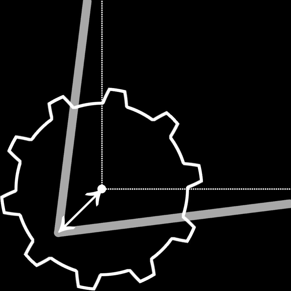
4 introduction The Beginning In Dec Richard Feynman offered a prize of $1,000. Challenge: build an electrical motor, each side smaller than 1 in 0.397mm 64 slide 4
")
5 introduction electrical motor by William McLellan diameter: 381μm tools used for assembly: microscope sharpened tooth pick hairs of a fine artist's brush McLellan's micromotor photographed under a microscope (Caltech Institute Archives) slide 5
6 progress 1. introduction 2. definition of MEMS & NEMS 2.1. What is MEMS? 2.2. What is NEMS? 2.3. problems with NEMS 3. active principles 4. types of MEMS 5. fabrication 6. problems with the fabrication slide 6
7 What is MEMS? MEMS - microelectromechanical systems transformation of energy: electricity light thermal. energy mechanical motion.. MEMS mainly move by elastic deformation of their flexible components. slide 7


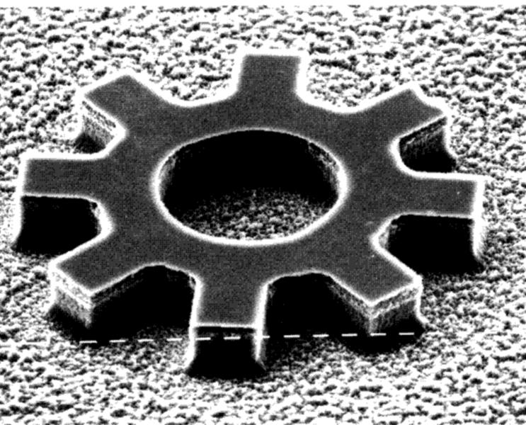
8 What is MEMS? spider mite (length: approx. 0.5mm) Courtesy of Sandia National Laboratories, SUMMiTTM Technologies, slide 8
9 What is NEMS? NEMS - nanoelectromechanical systems similar to MEMS but smaller (nanoscale) future prospects: ability to measure small displacements and forces at a molecular scale The border between MEMS and NEMS can hardly be defined: 500nm or 0.5μm? slide 9
10 problems with NEMS-technology It is possible to create structures with only several nanometers in size, BUT: nanoscale cantilevers/beams: a considerable big number of atoms are surface atoms interference with surrounding molecules additional physical effects have to be considered (e. g. increased influence of adhesion) just scaling down MEMS layouts does not work! slide 10
11 problems with NEMS-technology some examples: NEMS can respond to masses of single atoms: sensors could respond to impacts of molecules measurment of small deflection/forces also means small signals: difficulty to tell the signals apart from the noise adhesion of pieces that operate as capacitive electrodes could induce short circuits slide 11
12 problems with NEMS-technology effects, that are irrelevant to micro devices, have to be considered for nano devices new design approaches have to be found production and packaging have to take place in an extremely clean environment slide 12
13 progress 1. introduction 2. definition of MEMS & NEMS 3. active principles 3.1. thermal transduction 3.2. electrostatic transduction 3.3. piezo-resistive effect 4. types of MEMS 5. fabrication 6. problems with the fabrication slide 13

14 active principles thermal transduction A: E: α: cross-sectional area Young's modulus thermal coefficient F = Fb no displaceme nt change in length: Δ l=α l Δ T block force : Fb=E A α Δ T slide 14


15 active principles thermal transduction vertical motion moveable fixed bent beam actuator bi-metal actuator slide 15
16 active principles advantages & disadvantages of thermal transduction + large forces/displacements large input energies low frequencies slide 16
17 active principles electrostatic transduction parallel plate movement: Δ x comb finger movement: Δ A d comb fingers ΔA parallel plate d +Δ x x Δ U= Q εδa Δx Δ U=Q εa slide 17


18 active principles electrostatic transduction spring elements 75μm d parallel electrodes 10μm comb drives slide 18
19 active principles advantages & disadvantages of electrostatic transduction + fast response + easy integration with CMOS small actuation force slide 19

20 active principles piezo-resistive effect l Δ l V connect piezo actuator to voltage source change in length slide 20

21 active principles piezo-resistive effect F V compress or expand piezo sensor l Δ l potential difference F slide 21
22 active principles piezo-resistive effect in polysilicon ΔR R gauge factor K= Δl l thin film of polysilicon (p- or n-doped) isolator (e. g. SiO2, Si3N4) cantilever/beam/membrane slide 22
23 active principles piezo-resistive effect in polysilicon maximum gauge factor p-doped: 40 n-doped: 20 NA/D 1019cm-3 TCVD=560 C annealing: C slide 23
24 progress 1. introduction 2. definition of MEMS & NEMS 3. active principles 4. types of MEMS 4.1. sensors 4.2. actuators 5. fabrication 6. problems with the fabrication slide 24
25 types of MEMS sensors - accelerometers - gyroscopes actuators - micromirrors - droplet generator - microengines - micropumps slide 25
26 sensors: accelerometers accelerometers in automotive applications to activate safety systems and to implement vehicle stability systems hard disc protection systems... slide 26


27 sensors: accelerometers accelerometers a simple MEMS accelerometer is designed as followed: the proof mass is suspended by one to four silicon beams basic design and mechanical equivalent: suspension beams proof mass K m D proof mass a x reference frame slide 27


28 sensors: accelerometers accelerometers acceleration causes displacement of the proof mass displacement of the proof mass can be measured by strain gauges in the beams or change in capacitance suspension beams with strain gauges proof mass with capacitive electrodes slide 28

29 sensors: accelerometers accelerometers depending on the change in each capacitance, the threedimensional acceleration vector can be derived vertical acceleration horizontal acceleration slide 29
30 sensors: gyroscopes gyroscopes vibratory gyroscopes: transfer of energy between two vibration modes vibrating mechanical element: proof mass slide 30
31 sensors: gyroscopes gyroscopes ω Coriolis accelaration ac=2 ω v v a slide 31


32 sensors: gyroscopes tuning fork gyroscope rotation detection by capacitive electrodes under the proof mass a ω v Draper Lab comb drive tuning fork gyroscope slide 32


33 actuators: micromirrors micromirrors for phase modulation 16 μm slide 33


34 actuators: droplet generator nozzle membrane cooling hole ink reservoir heating element slide 34


35 actuators: microengines microengine with electrostaticly driven combdrives Courtesy of Sandia National Laboratories, SUMMiTTM Technologies, slide 35


36 actuators: microengines close-up view on different linkage designes Courtesy of Sandia National Laboratories, SUMMiTTM Technologies, slide 36


37 actuators: microengines torque : Mi=F r sin φi i φ1 r φ2 slide 37


38 actuators: micropumps micropump with piezo actuators frequency controlled flow rate slide 38
39 progress 1. introduction 2. definition of MEMS & NEMS 3. active principles 4. types of MEMS 5. fabrication 6. problems with the fabrication slide 39
40 fabrication epitaxial growth thermal oxidation (SiO2-layers) chemical vapour deposition thermal evaporation (metalic layers) electrolytic deposition slide 40

41 fabrication chemical vapour deposition (CVD) e. g. layer of phosphorus-doped silicon heated chamber wafers PH3 + SiH4 n-doped silicon layer slide 41


42 fabrication ultraviolet light mask photo resist Si, SiO2 etching plasma etching, KOH-etching (Si), HF-etching (SiO2),... minimum structure width: ultraviolet light: 1μm e-beam, x-ray: <1μm slide 42


43 fabrication etching isotropic e. g. SiO2 etched by HF e. g. <100> - Si etched by KOH anisotropic e. g. plasma etched Si slide 43
 selective etching rate: R { < 100 > - crystal plane} = 30 R {")
44 fabrication silicon wet etching (e. g. with KOH) selective etching rate: R { < 100 > - crystal plane} = 30 R { < 111 > - crystal plane} 1 slide 44

2 + H2")


45 fabrication silicon wet etching (e. g. with KOH) Si + 2 OH + 2 H2O SiO2(OH)2 + H2 silicon surface surface structure of <100> - silicon surface structure of <111> - silicon slide 45


46 fabrication reactive ion etching reactive ion etching: combines chemical and physikal etching e. g. flour ions react with silicon AND heavy ions impact on the surface attention: physical etching also attacks the pattern slide 46

47 fabrication reactive ion etching slide 47
48 fabrication reactive ion etching Si: SiO2: SiCl4, CCl4, BCl3, SF6 C2F6, CHF3 slide 48
49 progress 1. introduction 2. definition of MEMS & NEMS 3. active principles 4. types of MEMS 5. fabrication 6. problems with the fabrication slide 49
50 problems with the fabrication contamination microscopic contaminations (dust) molecular dirt: e. g. oil fog from vacuum pumps adhesion degradation of epitaxial layers slide 50
51 problems with the fabrication hillocks KOH-etching: dust particles may result in hillocks slide 51
52 list of references & picture credits N. Lobontiu, E. Garcia: Mechanics of Microelectromechanical Systems, Kluwer Academic Publishers, 2005 M. Glück: MEMS in der Mikrosystemtechnik, B.G. Teubner Verlag, Wiesbaden 2005 M. Elwenspoek, R. Wiegerink: Mechanical Microsensors, Springer-Verlag, Berlin 2001 M. Gad-el-Hak (editor): The MEMS Handbook, CRC Press, Boca Raton 2006 W. Lachermeier: Das Labor in der Westentasche, Mechatronik F&M, 3/ slide 52
Lecture 7 CMOS MEMS. CMOS MEMS Processes. CMOS MEMS Processes. Why CMOS-MEMS? Agenda: CMOS MEMS: Fabrication. MEMS structures can be made
 EEL6935 Advanced MEMS (Spring 2005) Instructor: Dr. Huikai Xie CMOS MEMS Agenda: Lecture 7 CMOS MEMS: Fabrication Pre-CMOS Intra-CMOS Post-CMOS Deposition Etching Why CMOS-MEMS? Smart on-chip CMOS circuitry
There are basically two approaches for bulk micromachining of. silicon, wet and dry. Wet bulk micromachining is usually carried out
 57 Chapter 3 Fabrication of Accelerometer 3.1 Introduction There are basically two approaches for bulk micromachining of silicon, wet and dry. Wet bulk micromachining is usually carried out using anisotropic
Lecture 5. SOI Micromachining. SOI MUMPs. SOI Micromachining. Silicon-on-Insulator Microstructures. Agenda:
 EEL6935 Advanced MEMS (Spring 2005) Instructor: Dr. Huikai Xie SOI Micromachining Agenda: SOI Micromachining SOI MUMPs Multi-level structures Lecture 5 Silicon-on-Insulator Microstructures Single-crystal
EE C245 ME C218 Introduction to MEMS Design Fall 2011
 Lecture Outline EE C245 ME C218 Introduction to MEMS Design Fall 2011 Prof. Clark T.-C. Nguyen Dept. of Electrical Engineering & Computer Sciences University of California at Berkeley Berkeley, CA 94720
Surface Micromachining
 Surface Micromachining Outline Introduction Material often used in surface micromachining Material selection criteria in surface micromachining Case study: Fabrication of electrostatic motor Major issues
Regents of the University of California
 Surface-Micromachining Process Flow Photoresist Sacrificial Oxide Structural Polysilcon Deposit sacrificial PSG: Target = 2 m 1 hr. 40 min. LPCVD @450 o C Densify the PSG Anneal @950 o C for 30 min. Lithography
EE40 Lec 22. IC Fabrication Technology. Prof. Nathan Cheung 11/19/2009
 Suggested Reading EE40 Lec 22 IC Fabrication Technology Prof. Nathan Cheung 11/19/2009 300mm Fab Tour http://www-03.ibm.com/technology/manufacturing/technology_tour_300mm_foundry.html Overview of IC Technology
Figure 2.3 (cont., p. 60) (e) Block diagram of Pentium 4 processor with 42 million transistors (2000). [Courtesy Intel Corporation.
 (e) Block diagram of Pentium 4 processor with 42 million transistors (2000). [Courtesy Intel Corporation.") Figure 2.1 (p. 58) Basic fabrication steps in the silicon planar process: (a) oxide formation, (b) selective oxide removal, (c) deposition of dopant atoms on wafer, (d) diffusion of dopant atoms into exposed
Figure 2.1 (p. 58) Basic fabrication steps in the silicon planar process: (a) oxide formation, (b) selective oxide removal, (c) deposition of dopant atoms on wafer, (d) diffusion of dopant atoms into exposed
Micro-Scale Engineering I Microelectromechanical Systems (MEMS) Y. C. Lee
 Y. C. Lee") Micro-Scale Engineering I Microelectromechanical Systems (MEMS) Y. C. Lee Department of Mechanical Engineering University of Colorado Boulder, CO 80309-0427 leeyc@colorado.edu September 2, 2008 1 Three
Micro-Scale Engineering I Microelectromechanical Systems (MEMS) Y. C. Lee Department of Mechanical Engineering University of Colorado Boulder, CO 80309-0427 leeyc@colorado.edu September 2, 2008 1 Three
Micro-Electro-Mechanical Systems (MEMS) Fabrication. Special Process Modules for MEMS. Principle of Sensing and Actuation
 Fabrication. Special Process Modules for MEMS. Principle of Sensing and Actuation") Micro-Electro-Mechanical Systems (MEMS) Fabrication Fabrication Considerations Stress-Strain, Thin-film Stress, Stiction Special Process Modules for MEMS Bonding, Cavity Sealing, Deep RIE, Spatial forming
Micro-Electro-Mechanical Systems (MEMS) Fabrication Fabrication Considerations Stress-Strain, Thin-film Stress, Stiction Special Process Modules for MEMS Bonding, Cavity Sealing, Deep RIE, Spatial forming
Surface micromachining and Process flow part 1
 Surface micromachining and Process flow part 1 Identify the basic steps of a generic surface micromachining process Identify the critical requirements needed to create a MEMS using surface micromachining
FABRICATION PROCESSES FOR MAGNETIC MICROACTUATORS WITH POLYSILICON FLEXURES. Jack W. Judy and Richard S. Muller
 FABRICATION PROCESSES FOR MAGNETIC MICROACTUATORS WITH POLYSILICON FLEXURES Jack W. Judy and Richard S. Muller Berkeley Sensor & Actuator Center (BSAC) Department of EECS, University of California, Berkeley,
ELEC 3908, Physical Electronics, Lecture 4. Basic Integrated Circuit Processing
 ELEC 3908, Physical Electronics, Lecture 4 Basic Integrated Circuit Processing Lecture Outline Details of the physical structure of devices will be very important in developing models for electrical behavior
Alternative Methods of Yttria Deposition For Semiconductor Applications. Rajan Bamola Paul Robinson
 Alternative Methods of Yttria Deposition For Semiconductor Applications Rajan Bamola Paul Robinson Origin of Productivity Losses in Etch Process Aggressive corrosive/erosive plasma used for etch Corrosion/erosion
Poly-SiGe MEMS actuators for adaptive optics
 Poly-SiGe MEMS actuators for adaptive optics Blake C.-Y. Lin a,b, Tsu-Jae King a, and Richard S. Muller a,b a Department of Electrical Engineering and Computer Sciences, b Berkeley Sensor and Actuator
Integrated Processes. Lecture Outline
 Integrated Processes Thara Srinivasan Lecture 14 Picture credit: Lemkin et al. Lecture Outline From reader Bustillo, J. et al., Surface micromachining of MEMS, pp. 1556-9. A.E. Franke et al., Polycrystalline
March 10th. Frog, Water Strider, Gecko. Elephant vs. Ant Design & Manufacturing II. Ask Dave and Pat. Spring Quiz 1 on March 17 th MEMS I
 P O O O O O O O O O O O O O O O O O O O O O O O S S S S S S S S Office of Basic Energy Sciences Office of Science, U.S. DOE Version 03-05-02 2.008 Design & Manufacturing II Spring 2004 MEMS I March 10th
Gaetano L Episcopo. Introduction to MEMS
 Gaetano L Episcopo Introduction to MEMS What are MEMS? Micro Electro Mechanichal Systems MEMS are integrated devices, or systems of devices, with microscopic parts, such as: Mechanical Parts Electrical
SURFACE MICROMACHINING
 SURFACE MICROMACHINING Features are built up, layer by layer on the surface of a substrate. Surface micromachined devices are much smaller than bulk micromachined components. Nature of deposition process
FABRICATION ENGINEERING MICRO- NANOSCALE ATTHE AND. Fourth Edition STEPHEN A. CAMPBELL. of Minnesota. University OXFORD UNIVERSITY PRESS
 AND FABRICATION ENGINEERING ATTHE MICRO- NANOSCALE Fourth Edition STEPHEN A. CAMPBELL University of Minnesota New York Oxford OXFORD UNIVERSITY PRESS CONTENTS Preface xiii prrt i OVERVIEW AND MATERIALS
Microstructures using RF sputtered PSG film as a sacrificial layer in surface micromachining
 Sādhanā Vol. 34, Part 4, August 2009, pp. 557 562. Printed in India Microstructures using RF sputtered PSG film as a sacrificial layer in surface micromachining VIVEKANAND BHATT 1,, SUDHIR CHANDRA 1 and
CMOS FABRICATION. n WELL PROCESS
 CMOS FABRICATION n WELL PROCESS Step 1: Si Substrate Start with p- type substrate p substrate Step 2: Oxidation Exposing to high-purity oxygen and hydrogen at approx. 1000 o C in oxidation furnace SiO
Procese de depunere in sistemul Plasma Enhanced Chemical Vapor Deposition (PECVD)
") Procese de depunere in sistemul Plasma Enhanced Chemical Vapor Deposition (PECVD) Ciprian Iliescu Conţinutul acestui material nu reprezintă in mod obligatoriu poziţia oficială a Uniunii Europene sau a
Procese de depunere in sistemul Plasma Enhanced Chemical Vapor Deposition (PECVD) Ciprian Iliescu Conţinutul acestui material nu reprezintă in mod obligatoriu poziţia oficială a Uniunii Europene sau a
Bulk Silicon Micromachining
 Bulk Silicon Micromachining Micro Actuators, Sensors, Systems Group University of Illinois at Urbana-Champaign Outline Types of bulk micromachining silicon anisotropic etching crystal orientation isotropic
VLSI Technology. By: Ajay Kumar Gautam
 By: Ajay Kumar Gautam Introduction to VLSI Technology, Crystal Growth, Oxidation, Epitaxial Process, Diffusion Process, Ion Implantation, Lithography, Etching, Metallization, VLSI Process Integration,
Growth and Doping of SiC-Thin Films on Low-Stress, Amorphous Si 3 N 4 /Si Substrates for Robust Microelectromechanical Systems Applications
 Journal of ELECTRONIC MATERIALS, Vol. 31, No. 5, 2002 Special Issue Paper Growth and Doping of SiC-Thin Films on Low-Stress, Amorphous Si 3 N 4 /Si Substrates for Robust Microelectromechanical Systems
Semiconductor Manufacturing Technology. IC Fabrication Process Overview
 Semiconductor Manufacturing Technology Michael Quirk & Julian Serda October 00 by Prentice Hall Chapter 9 IC Fabrication Process Overview /4 Objectives After studying the material in this chapter, you
Atomic Layer Deposition(ALD)
") Atomic Layer Deposition(ALD) AlO x for diffusion barriers OLED displays http://en.wikipedia.org/wiki/atomic_layer_deposition#/media/file:ald_schematics.jpg Lam s market-leading ALTUS systems combine CVD
Atomic Layer Deposition(ALD) AlO x for diffusion barriers OLED displays http://en.wikipedia.org/wiki/atomic_layer_deposition#/media/file:ald_schematics.jpg Lam s market-leading ALTUS systems combine CVD
ME 189 Microsystems Design and Manufacture. Chapter 9. Micromanufacturing
 ME 189 Microsystems Design and Manufacture Chapter 9 Micromanufacturing This chapter will offer an overview of the application of the various fabrication techniques described in Chapter 8 in the manufacturing
Lecture 22: Integrated circuit fabrication
 Lecture 22: Integrated circuit fabrication Contents 1 Introduction 1 2 Layering 4 3 Patterning 7 4 Doping 8 4.1 Thermal diffusion......................... 10 4.2 Ion implantation.........................
Proceedings Post Fabrication Processing of Foundry MEMS Structures Exhibiting Large, Out-of-Plane Deflections
 Proceedings Post Fabrication Processing of Foundry MEMS Structures Exhibiting Large, Out-of-Plane Deflections LaVern Starman 1, *, John Walton 1, Harris Hall 1 and Robert Lake 2 1 Sensors Directorate,
4/10/2012. Introduction to Microfabrication. Fabrication
 Introduction to Microfabrication Fabrication 1 MEMS Fabrication Flow Basic Process Flow in Micromachining Nadim Maluf, An introduction to Microelectromechanical Systems Engineering 2 Thin Film Deposition
Sensors and Actuators Designed and Fabricated in a. Micro-Electro-Mechanical-Systems (MEMS) Course. Using Standard MEMS Processes
 Course. Using Standard MEMS Processes") Sensors and Actuators Designed and Fabricated in a Micro-Electro-Mechanical-Systems (MEMS) Course Using Standard MEMS Processes M.G. Guvench University of Southern Maine guvench@maine.edu Abstract Use
Sensors and Actuators Designed and Fabricated in a Micro-Electro-Mechanical-Systems (MEMS) Course Using Standard MEMS Processes M.G. Guvench University of Southern Maine guvench@maine.edu Abstract Use
HOMEWORK 4 and 5. March 15, Homework is due on Monday March 30, 2009 in Class. Answer the following questions from the Course Textbook:
 HOMEWORK 4 and 5 March 15, 2009 Homework is due on Monday March 30, 2009 in Class. Chapter 7 Answer the following questions from the Course Textbook: 7.2, 7.3, 7.4, 7.5, 7.6*, 7.7, 7.9*, 7.10*, 7.16, 7.17*,
Metallization deposition and etching. Material mainly taken from Campbell, UCCS
 Metallization deposition and etching Material mainly taken from Campbell, UCCS Application Metallization is back-end processing Metals used are aluminum and copper Mainly involves deposition and etching,
NANOINDENTATION OF SILICON CARBIDE WAFER COATINGS
 NANOINDENTATION OF SILICON CARBIDE WAFER COATINGS Prepared by Jesse Angle 6 Morgan, Ste156, Irvine CA 9618 P: 949.461.99 F: 949.461.93 nanovea.com Today's standard for tomorrow's materials. 010 NANOVEA
Materials for MEMS. Dr. Yael Hanein. 11 March 2004 Materials Applications Yael Hanein
 Materials for MEMS Dr. Yael Hanein Materials for MEMS MEMS (introduction) Materials used in MEMS Material properties Standard MEMS processes MEMS The world s smallest guitar is about 10 micrometers long
Lecture 10: MultiUser MEMS Process (MUMPS)
") MEMS: Fabrication Lecture 10: MultiUser MEMS Process (MUMPS) Prasanna S. Gandhi Assistant Professor, Department of Mechanical Engineering, Indian Institute of Technology, Bombay, 1 Recap Various VLSI based
MEMS: Fabrication Lecture 10: MultiUser MEMS Process (MUMPS) Prasanna S. Gandhi Assistant Professor, Department of Mechanical Engineering, Indian Institute of Technology, Bombay, 1 Recap Various VLSI based
6.777J/2.732J Design and Fabrication of Microelectromechanical Devices Spring Term Solution to Problem Set 2 (16 pts)
") 6.777J/2.732J Design and Fabrication of Microelectromechanical Devices Spring Term 2007 By Brian Taff (Adapted from work by Feras Eid) Solution to Problem Set 2 (16 pts) Issued: Lecture 4 Due: Lecture
6.777J/2.732J Design and Fabrication of Microelectromechanical Devices Spring Term 2007 By Brian Taff (Adapted from work by Feras Eid) Solution to Problem Set 2 (16 pts) Issued: Lecture 4 Due: Lecture
VLSI INTRODUCTION P.VIDYA SAGAR ( ASSOCIATE PROFESSOR) Department of Electronics and Communication Engineering, VBIT
 Department of Electronics and Communication Engineering, VBIT") VLSI INTRODUCTION P.VIDYA SAGAR ( ASSOCIATE PROFESSOR) contents UNIT I INTRODUCTION: Introduction to IC Technology MOS, PMOS, NMOS, CMOS & BiCMOS technologies. BASIC ELECTRICAL PROPERTIES : Basic Electrical
VLSI INTRODUCTION P.VIDYA SAGAR ( ASSOCIATE PROFESSOR) contents UNIT I INTRODUCTION: Introduction to IC Technology MOS, PMOS, NMOS, CMOS & BiCMOS technologies. BASIC ELECTRICAL PROPERTIES : Basic Electrical
Chapter 2. Density 2.65 g/cm 3 Melting point Young s modulus Tensile strength Thermal conductivity Dielectric constant 3.
 Chapter 2 Thin Film Materials Thin films of Silicon dioxide, Silicon nitride and Polysilicon have been utilized in the fabrication of absolute micro pressure sensor. These materials are studied and discussed
5.8 Diaphragm Uniaxial Optical Accelerometer
 5.8 Diaphragm Uniaxial Optical Accelerometer Optical accelerometers are based on the BESOI (Bond and Etch back Silicon On Insulator) wafers, supplied by Shin-Etsu with (100) orientation, 4 diameter and
Dr. Priyabrat Dash Office: BM-406, Mob: Webpage: MB: 205
 Email: dashp@nitrkl.ac.in Office: BM-406, Mob: 8895121141 Webpage: http://homepage.usask.ca/~prd822/ MB: 205 Nonmanufacturing In continuation from last class... 2 Top-Down methods Mechanical-energy methods
EE 434 Lecture 9. IC Fabrication Technology
 EE 434 Lecture 9 IC Fabrication Technology Quiz 7 The layout of a film resistor with electrodes A and B is shown. If the sheet resistance of the film is 40 /, determine the resistance between nodes A and
Applications of High-Performance MEMS Pressure Sensors Based on Dissolved Wafer Process
 Applications of High-Performance MEMS Pressure Sensors Based on Dissolved Wafer Process Srinivas Tadigadapa and Sonbol Massoud-Ansari Integrated Sensing Systems (ISSYS) Inc., 387 Airport Industrial Drive,
3. Overview of Microfabrication Techniques
 3. Overview of Microfabrication Techniques The Si revolution First Transistor Bell Labs (1947) Si integrated circuits Texas Instruments (~1960) Modern ICs More? Check out: http://www.pbs.org/transistor/background1/events/miraclemo.html
3.155J / 6.152J Micro/Nano Processing Technology TAKE-HOME QUIZ FALL TERM 2005
 3.155J / 6.152J Micro/Nano Processing Technology TAKE-HOME QUIZ FALL TERM 2005 1) This is an open book, take-home quiz. You are not to consult with other class members or anyone else. You may discuss the
Surface Micromachining II
 Surface Micromachining II Dr. Thara Srinivasan Lecture 4 Picture credit: Sandia National Lab Lecture Outline Reading From reader: Bustillo, J. et al., Surface Micromachining of Microelectromechanical Systems,
Lecture Day 2 Deposition
 Deposition Lecture Day 2 Deposition PVD - Physical Vapor Deposition E-beam Evaporation Thermal Evaporation (wire feed vs boat) Sputtering CVD - Chemical Vapor Deposition PECVD LPCVD MVD ALD MBE Plating
Process Flow in Cross Sections
 Process Flow in Cross Sections Process (simplified) 0. Clean wafer in nasty acids (HF, HNO 3, H 2 SO 4,...) --> wear gloves! 1. Grow 500 nm of SiO 2 (by putting the wafer in a furnace with O 2 2. Coat
Nanoscale Imaging, Material Removal and Deposition for Fabrication of Cutting-edge Semiconductor Devices
 Hitachi Review Vol. 65 (2016), No. 7 233 Featured Articles Nanoscale Imaging, Material Removal and Deposition for Fabrication of Cutting-edge Semiconductor Devices Ion-beam-based Photomask Defect Repair
The Surface/Bulk Micromachining (SBM) Process: A New Method for Fabricating Released MEMS in Single Crystal Silicon
 Process: A New Method for Fabricating Released MEMS in Single Crystal Silicon") JOURNAL OF MICROELECTROMECHANICAL SYSTEMS, VOL. 8, NO. 4, DECEMBER 1999 409 The Surface/Bulk Micromachining (SBM) Process: A New Method for Fabricating Released MEMS in Single Crystal Silicon Sangwoo Lee,
JOURNAL OF MICROELECTROMECHANICAL SYSTEMS, VOL. 8, NO. 4, DECEMBER 1999 409 The Surface/Bulk Micromachining (SBM) Process: A New Method for Fabricating Released MEMS in Single Crystal Silicon Sangwoo Lee,
Silicon Manufacturing
 Silicon Manufacturing Group Members Young Soon Song Nghia Nguyen Kei Wong Eyad Fanous Hanna Kim Steven Hsu th Fundamental Processing Steps 1.Silicon Manufacturing a) Czochralski method. b) Wafer Manufacturing
Midterm evaluations. Nov. 9, J/3.155J 1
 Midterm evaluations What learning activities were found most helpful Example problems, case studies (5); graphs (good for extracting useful info) (4); Good interaction (2); Good lecture notes, slides (2);
Overview. Silicon Microfabrication Part 2. Introduction to BioMEMS & Medical Microdevices
 Introduction to BioMEMS & Medical Microdevices Silicon Microfabrication Part 2 Companion lecture to the textbook: Fundamentals of BioMEMS and Medical Microdevices, by Prof., http://saliterman.umn.edu/
Silicon Microfabrication Part 2
 Introduction to BioMEMS & Medical Microdevices Silicon Microfabrication Part 2 Companion lecture to the textbook: Fundamentals of BioMEMS and Medical Microdevices, by Prof., http://saliterman.umn.edu/
Lecture 19 Microfabrication 4/1/03 Prof. Andy Neureuther
 EECS 40 Spring 2003 Lecture 19 Microfabrication 4/1/03 Prof. ndy Neureuther How are Integrated Circuits made? Silicon wafers Oxide formation by growth or deposition Other films Pattern transfer by lithography
Fabrication Technology
 Fabrication Technology By B.G.Balagangadhar Department of Electronics and Communication Ghousia College of Engineering, Ramanagaram 1 OUTLINE Introduction Why Silicon The purity of Silicon Czochralski
Microfabrication of Heterogeneous, Optimized Compliant Mechanisms SUNFEST 2001 Luo Chen Advisor: Professor G.K. Ananthasuresh
 Microfabrication of Heterogeneous, Optimized Compliant Mechanisms SUNFEST 2001 Luo Chen Advisor: Professor G.K. Ananthasuresh Fig. 1. Single-material Heatuator with selective doping on one arm (G.K. Ananthasuresh)
Ion Implantation Most modern devices doped using ion implanters Ionize gas sources (single +, 2+ or 3+ ionization) Accelerate dopant ions to very
 Accelerate dopant ions to very") Ion Implantation Most modern devices doped using ion implanters Ionize gas sources (single +, 2+ or 3+ ionization) Accelerate dopant ions to very high voltages (10-600 KeV) Use analyzer to selection charge/mass
Ion Implantation Most modern devices doped using ion implanters Ionize gas sources (single +, 2+ or 3+ ionization) Accelerate dopant ions to very high voltages (10-600 KeV) Use analyzer to selection charge/mass
Sensor. Device that converts a non-electrical physical or chemical quantity into an electrical signal. Sensor Processor Display Output signal
 Microsensors Outline Sensor & microsensor Force and pressure microsensors Position and speed microsensors Acceleration microsensors Chemical microsensors Biosensors Temperature sensors Sensor Device that
CMOS Manufacturing process. Circuit designer. Design rule set. Process engineer. Set of optical masks. Fabrication process.
 CMOS Manufacturing process Circuit design Set of optical masks Fabrication process Circuit designer Design rule set Process engineer All material: Chap. 2 of J. Rabaey, A. Chandrakasan, B. Nikolic, Digital
Ajay Kumar Gautam [VLSI TECHNOLOGY] VLSI Technology for 3RD Year ECE/EEE Uttarakhand Technical University
![Ajay Kumar Gautam [VLSI TECHNOLOGY] VLSI Technology for 3RD Year ECE/EEE Uttarakhand Technical University](/thumbs/75/72824557.jpg "Ajay Kumar Gautam [VLSI TECHNOLOGY] VLSI Technology for 3RD Year ECE/EEE Uttarakhand Technical University") 2014 Ajay Kumar Gautam [VLSI TECHNOLOGY] VLSI Technology for 3RD Year ECE/EEE Uttarakhand Technical University Page1 Syllabus UNIT 1 Introduction to VLSI Technology: Classification of ICs, Scale of integration,
2014 Ajay Kumar Gautam [VLSI TECHNOLOGY] VLSI Technology for 3RD Year ECE/EEE Uttarakhand Technical University Page1 Syllabus UNIT 1 Introduction to VLSI Technology: Classification of ICs, Scale of integration,
Basic&Laboratory& Materials&Science&and&Engineering& Micro&Electromechanical&Systems&& (MEMS)&
&") Basic&Laboratory& Materials&Science&and&Engineering& Micro&Electromechanical&Systems&& (MEMS)& M105& As of: 27.10.2011 1 Introduction... 2 2 Materials used in MEMS fabrication... 2 3 MEMS fabrication processes...
Basic&Laboratory& Materials&Science&and&Engineering& Micro&Electromechanical&Systems&& (MEMS)& M105& As of: 27.10.2011 1 Introduction... 2 2 Materials used in MEMS fabrication... 2 3 MEMS fabrication processes...
Silver Diffusion Bonding and Layer Transfer of Lithium Niobate to Silicon
 Chapter 5 Silver Diffusion Bonding and Layer Transfer of Lithium Niobate to Silicon 5.1 Introduction In this chapter, we discuss a method of metallic bonding between two deposited silver layers. A diffusion
KGC SCIENTIFIC Making of a Chip
 KGC SCIENTIFIC www.kgcscientific.com Making of a Chip FROM THE SAND TO THE PACKAGE, A DIAGRAM TO UNDERSTAND HOW CPU IS MADE? Sand CPU CHAIN ANALYSIS OF SEMICONDUCTOR Material for manufacturing process
Surface Micromachining Process for the Integration of AlN Piezoelectric Microstructures
 Surface Micromachining Process for the Integration of AlN Piezoelectric Microstructures Saravanan. S, Erwin Berenschot, Gijs Krijnen and Miko Elwenspoek Transducers Science and Technology Laboratory University
Design and fabrication of MEMS devices using the integration of MUMPs, trench-refilled molding, DRIE and bulk silicon etching processes
 TB, KR, JMM/184987, 3/12/2004 INSTITUTE OF PHYSICS PUBLISHING JOURNAL OF MICROMECHANICS AND MICROENGINEERING J. Micromech. Microeng. 15 (2005) 1 8 doi:10.1088/0960-1317/15/0/000 Design and fabrication
Calibration technique for MEMS membrane type strain sensors
 Calibration technique for MEMS membrane type strain sensors Li Cao a, Tae Song Kim b, Jia Zhou a, Susan C. Mantell a *, and Dennis L. Polla b a Dept. of Mechanical Engineering, University of Minnesota,
MEMS prototyping using RF sputtered films
 Indian Journal of Pure & Applied Physics Vol. 45, April 2007, pp. 326-331 MEMS prototyping using RF sputtered films Sudhir Chandra, Vivekanand Bhatt, Ravindra Singh, Preeti Sharma & Prem Pal* Centre for
Co-Evolution of Stress and Structure During Growth of Polycrystalline Thin Films
 Co-Evolution of Stress and Structure During Growth of Polycrystalline Thin Films Carl V. Thompson and Hang Z. Yu* Dept. of Materials Science and Engineering MIT, Cambridge, MA, USA Effects of intrinsic
Ion Implantation Most modern devices doped using ion implanters Implant dopants by accelerating individual atoms (ions) Ionize gas sources (single +,
 Ionize gas sources (single +,") Ion Implantation Most modern devices doped using ion implanters Implant dopants by accelerating individual atoms (ions) Ionize gas sources (single +, 2+ or 3+ ionization) Use analyzer to selection charge/mass
Ion Implantation Most modern devices doped using ion implanters Implant dopants by accelerating individual atoms (ions) Ionize gas sources (single +, 2+ or 3+ ionization) Use analyzer to selection charge/mass
Evaluation of length scale effects for micro and nano-sized cantilevered structures
 University of Wollongong Research Online University of Wollongong Thesis Collection 1954-2016 University of Wollongong Thesis Collections 2010 Evaluation of length scale effects for micro and nano-sized
Process steps for Field Emitter devices built on Silicon wafers And 3D Photovoltaics on Silicon wafers
 Process steps for Field Emitter devices built on Silicon wafers And 3D Photovoltaics on Silicon wafers David W. Stollberg, Ph.D., P.E. Research Engineer and Adjunct Faculty GTRI_B-1 Field Emitters GTRI_B-2
ENG/PHYS3320 Microsystems Technology Chapter 2 Fabrication of Microsystems
 ENG/PHYS3320 Microsystems Technology Chapter 2 Fabrication of Microsystems ENG/PHYS3320: R.I. Hornsey Fab: 1 Fabrication Many of the new transducers are based on a technology known as micromachining a
FP7 piezovolume High Volume Piezoelectric Thin Film Production Process for Microsystems
 How to make an "old" material class the cutting edge FP7 piezovolume High Volume Piezoelectric Thin Film Production Process for Microsystems Frode Tyholdt (SINTEF) Piezoelectric microsystems (piezomems)
Preprint - Mechatronics 2008, Le Grand-Bornand, France, May
 Potentialities of piezoresistive cantilever force sensors based on free standing thick films Hélène Debéda(*), Isabelle Dufour, Patrick Ginet, Claude Lucat University of Bordeaux 1, IMS Laboratory, 51
ME 141B: The MEMS Class Introduction to MEMS and MEMS Design. Sumita Pennathur UCSB
 ME 141B: The MEMS Class Introduction to MEMS and MEMS Design Sumita Pennathur UCSB Outline today Introduction to thin films Oxidation Deal-grove model CVD Epitaxy Electrodeposition 10/6/10 2/45 Creating
Nanosensors. Rachel Heil 12/7/07 Wentworth Institute of Technology Department of Electronics and Mechanical Professor Khabari Ph.D.
 Nanosensors Rachel Heil 12/7/07 Wentworth Institute of Technology Department of Electronics and Mechanical Professor Khabari Ph.D. There are many advances in nanotechnology that if perfected could help
Fabrication and Layout
 ECEN454 Digital Integrated Circuit Design Fabrication and Layout ECEN 454 3.1 A Glimpse at MOS Device Polysilicon Aluminum ECEN 475 4.2 1 Material Classification Insulators Glass, diamond, silicon oxide
MOVING AND NON-MOVING MICRO PUMPS FOR FLUID DELIVERY: A STUDY OF CURRENT TECHNOLOGIES. ME2082 Dr. Wang Class Project Presenter: Susan Felix
 MOVING AND NON-MOVING MICRO PUMPS FOR FLUID DELIVERY: A STUDY OF CURRENT TECHNOLOGIES ME2082 Dr. Wang Class Project Presenter: Susan Felix Introduction! Micropump History! In existence since before 1970s!
EEC 118 Lecture #5: MOS Fabrication. Rajeevan Amirtharajah University of California, Davis Jeff Parkhurst Intel Corporation
 EEC 118 Lecture #5: MOS Fabrication Rajeevan Amirtharajah University of California, Davis Jeff Parkhurst Intel Corporation Announcements Lab 3 this week, report due next week HW 3 due this Friday at 4
Metallization. Typical current density ~10 5 A/cm 2 Wires introduce parasitic resistance and capacitance
 Metallization Interconnects Typical current density ~10 5 A/cm 2 Wires introduce parasitic resistance and capacitance RC time delay Inter-Metal Dielectric -Prefer low dielectric constant to reduce capacitance
3D Finite Element Modeling and Analysis of Micromechanical Sensors
 Abstract 3D Finite Element Modeling and Analysis of Micromechanical Sensors Alexey I. Borovkov, Eugeny V. Pereyaslavets Computational Mechanics Laboratory, St. Petersburg State Technical University, Russia
Thin Films: Sputtering Systems (Jaeger Ch 6 & Ruska Ch 7,) Can deposit any material on any substrate (in principal) Start with pumping down to high
 Can deposit any material on any substrate (in principal) Start with pumping down to high") Thin Films: Sputtering Systems (Jaeger Ch 6 & Ruska Ch 7,) Can deposit any material on any substrate (in principal) Start with pumping down to high vacuum ~10-7 torr Removes residual gases eg oxygen from
Thin Films: Sputtering Systems (Jaeger Ch 6 & Ruska Ch 7,) Can deposit any material on any substrate (in principal) Start with pumping down to high vacuum ~10-7 torr Removes residual gases eg oxygen from
EQUIPMENT AND SYSTEM FOR VACUUM COATING METALLIZING, SPUTTERING, PLASMA and PECVD. Hybrid system KOLZER DGK 36
 email : carlo.gennari@fastwebnet.it web site : http://carlogennariforni.beepworld.it/kolzer.htm EQUIPMENT AND SYSTEM FOR VACUUM COATING METALLIZING, SPUTTERING, PLASMA and PECVD Hybrid system KOLZER DGK
Plasma-Enhanced Chemical Vapor Deposition
 Plasma-Enhanced Chemical Vapor Deposition Steven Glenn July 8, 2009 Thin Films Lab 4 ABSTRACT The objective of this lab was to explore lab and the Applied Materials P5000 from a different point of view.
Semiconductor Technology
 Semiconductor Technology from A to Z Oxidation www.halbleiter.org Contents Contents List of Figures List of Tables II III 1 Oxidation 1 1.1 Overview..................................... 1 1.1.1 Application...............................
Isolation Technology. Dr. Lynn Fuller
 ROCHESTER INSTITUTE OF TECHNOLOGY MICROELECTRONIC ENGINEERING Isolation Technology Dr. Lynn Fuller Motorola Professor 82 Lomb Memorial Drive Rochester, NY 14623-5604 Tel (585) 475-2035 Fax (585) 475-5041
R Sensor resistance (Ω) ρ Specific resistivity of bulk Silicon (Ω cm) d Diameter of measuring point (cm)
 ρ Specific resistivity of bulk Silicon (Ω cm) d Diameter of measuring point (cm)") 4 Silicon Temperature Sensors 4.1 Introduction The KTY temperature sensor developed by Infineon Technologies is based on the principle of the Spreading Resistance. The expression Spreading Resistance derives
4 Silicon Temperature Sensors 4.1 Introduction The KTY temperature sensor developed by Infineon Technologies is based on the principle of the Spreading Resistance. The expression Spreading Resistance derives
VLSI Systems and Computer Architecture Lab
 ΚΥΚΛΩΜΑΤΑ VLSI Πανεπιστήμιο Ιωαννίνων CMOS Technology Τμήμα Μηχανικών Η/Υ και Πληροφορικής 1 From the book: An Introduction ti to VLSI Process By: W. Maly ΚΥΚΛΩΜΑΤΑ VLSI Διάρθρωση 1. N well CMOS 2. Active
Uncrosslinked SU-8 as a sacrificial material
 INSTITUTE OFPHYSICS PUBLISHING JOURNAL OF MICROMECHANICS AND MICROENGINEERING J. Micromech. Microeng. 15 (2005) N1 N5 doi:10.1088/0960-1317/15/1/n01 TECHNICAL NOTE Uncrosslinked as a sacrificial material
Ultra High Barrier Coatings by PECVD
 Society of Vacuum Coaters 2014 Technical Conference Presentation Ultra High Barrier Coatings by PECVD John Madocks & Phong Ngo, General Plasma Inc., 546 E. 25 th Street, Tucson, Arizona, USA Abstract Silicon
Measurement of thickness of native silicon dioxide with a scanning electron microscope
 Measurement of thickness of native silicon dioxide with a scanning electron microscope V. P. Gavrilenko* a, Yu. A. Novikov b, A. V. Rakov b, P. A. Todua a a Center for Surface and Vacuum Research, 40 Novatorov
Plasma Etching Rates & Gases Gas ratios affects etch rate & etch ratios to resist/substrate
 Plasma Etching Rates & Gases Gas ratios affects etch rate & etch ratios to resist/substrate Development of Sidewalls Passivating Films Sidewalls get inert species deposited on them with plasma etch Creates
Specimen Preparation Technique for a Microstructure Analysis Using the Focused Ion Beam Process
 Specimen Preparation Technique for a Microstructure Analysis Using the Focused Ion Beam Process by Kozue Yabusaki * and Hirokazu Sasaki * In recent years the FIB technique has been widely used for specimen
Silicon Wafer Processing PAKAGING AND TEST
 Silicon Wafer Processing PAKAGING AND TEST Parametrical test using test structures regularly distributed in the wafer Wafer die test marking defective dies dies separation die fixing (not marked as defective)
EE C245 ME C218 Introduction to MEMS Design Fall 2010
 Lecture Outline EE C245 ME C218 Introduction to MEMS Design Fall 2010 Prof. Clark T.-C. Nguyen Dept. of Electrical Engineering & Computer Sciences University of California at Berkeley Berkeley, CA 94720
Single crystal silicon supported thin film micromirrors for optical applications
 Single crystal silicon supported thin film micromirrors for optical applications Zhimin J. Yao* Noel C. MacDonald Cornell University School of Electrical Engineering and Cornell Nanofabrication Facility
HYPRES. Hypres MCM Process Design Rules 04/12/2016
 HYPRES Hypres MCM Process Design Rules 04/12/2016 Direct all inquiries, questions, comments and suggestions concerning these design rules and/or HYPRES fabrication to: Daniel T. Yohannes Tel. (914) 592-1190