Why SiO 2? The extraordinary properties of SiO 2 are the basis of the success of MOS-technology
|
|
|
- Chad Atkinson
- 5 years ago
- Views:
Transcription
1 Oxidation 1
2 Why? The extraordinary properties of are the basis of the success of MOS-technology Non-crystalline insulator Very high energy gap Φ M Easy to grow on Easy to integrate in a process E M Excellent interface between substrate Stable and insensitive to following process-steps Excellent scaling possibilities no real candidates for replacement E 0 1.0eV χ ox 9.0eV 3.0eV 4.9eV Φ S χ si E C E V 2
 Dielectric constant: 3.9 Energy gap : 9 ev Density : 2.20 g/cm 3 Refractive Index : ~1.")
3 Properties of - : 3.12 Å, -O: 1.62 Å, O-O: 2.27 Å 10 nm : atomic layers 1.2 nm : only about 4 atomic layers Bonding angle : 110~180 ( 144 ) Dielectric constant: 3.9 Energy gap : 9 ev Density : 2.20 g/cm 3 Refractive Index : ~1.462 Dielectric strength MV/cm Tetrahedra structure θ Bridging Oxygen Oxygen licon 3

4 Application of Thermal Oxides 4
5 Transistor Process Flow (1970s) Al nmos Cross-section PSG poly n + n + p- N Clean p- p- Field Oxidation Oxide Etch p- p- Gate Oxidation Poly Dep. p- poly p- poly Poly Etch P + Ion Implant p- poly n + poly p- n + Annealing 5
6 Masking Oxide Much lower B and P diffusion rates in than that in can be used as diffusion mask Dopant 6
7 Pad Oxide Relieve strong tensile stress of the nitride Prevent stress induced silicon defects licon nitride Pad Oxide licon Substrate 7
8 Blanket Field Oxide Isolation licon Wafer Clean licon Dioxide licon Activation Area Field Oxidation Field Oxide licon Oxide Etch 8
 E BD > 8MV/cm, pinhole free and negligible defects Sufficient long lifetime under normal operating High resistance to hot-carrier damage")
9 Gate Oxide Thickness of oxide (T ox ) must closely match the specification of the MOSFET design T ox must be sufficiently uniform across the entire wafer, and from wafer to wafer, and from run-to-run Extremely low Q f and D it (Good / interfacial properties) E BD > 8MV/cm, pinhole free and negligible defects Sufficient long lifetime under normal operating High resistance to hot-carrier damage Resistance to boron penetration Refer to Dr. Hong Xiao V G V D > 0 Poly Gate Thin oxide n + Source Electrons p- n + Drain Substrate Source: Dr. PT Liu 9
10 Growth Mechanism Native oxide: surface has a high affinity for oxygen formed in the air or chemical cleaning process quality is bad and should be eliminated Å Thermal oxidation: Dry Oxidation ( solid) + O O ( solid) 2 2 Wet Oxidation (steam oxide) ( solid) + 2 H O O ( solid) + 2H
11 1000 o C + Dry Oxidation Original licon Surface licon Dioxide ( ) 55% 45% licon wafer () Thickness of silicon = 0.45 x (thickness of ) substrate substrate Oxidizing species diffuse through to / Source: Dr. PT Liu 11
12 Oxide Growth: Deal-Grove Model Deal-Grove Relation (linear-parabolic growth law): Linear Growth (Reaction-Limited) Regime B Oxide Thickness X = t A Diffusion-limited Regime X = B t t ox t 0.44 t ox Top oxide surface Original silicon surface Oxidation Time licon Oxide-silicon surface 12
13 Growth Mechanism Deal-Grove Relation (linear-parabolic growth law): 2 ox T + AT = B( t+ τ ) 2 Tox = Bt ox for t >> τ, t >> A 2 /4B Diffusion-controlled for (t+ τ) << A 2 /4B T ox B = ( t+τ ) A Reaction-controlled * DC x + Ax i i A= 2 D[ + ] B= τ = k h N B A, B : temperature, ambient composition, pressure and crystalline orientation τ is related to the initial oxide thickness s I C g Gas phase C g Gas phase Reaction control F 1 Concentration Diffusion control F 1 C 0 Concentration C 0 F 2 F 2 C* F 3 X 0 X 0 C* C i C i + F
14 <100> licon Dry Oxidation Oxide Thickness (micron) <100> licon Dry Oxidation 1200 C 1150 C 1100 C 1050 C 1000 C 950 C 900 C Oxidation Time (hours) 14
15 Interfacial Structure Dangling bond surface Interfacial trap impurity Oxygen vacancy Stretched bond 15

16 Interfacial Structure bulk-oxide count TEM boundary total Oxygen count sub-oxide count t ox D. Muller, et. al, Nature, 399, 758(1999) 16
17 Oxide Traps and Defects Mobile Ionic Charge K + Na + Oxide Trapped Charge Fixed Oxide Charge Interface Trapped Charge (Deal, 1980) Fixed Charge (Q f, N f ) (Positive): structural defects due to incomplete oxidation and stress, within 2.5 nm from / not electrically communicate with interface states Mobile Oxide Charge (Q m, N m ): Na +, Li +,K +,H + Oxide Trapped Charge (Q ot,n ot ): positive or negative due to hole or electron traps in borken -O bonds radiation, charge injection in high field Interface Trapped Charge (Q it,n it, D it ): structural defects due to incomplete oxidation at / donor or acceptor-like surface-potential dependent 17
18 / Interface Interface states: imperfect bonds Electrically interacted with channel carriers Assuming each dangling bond give rise to one interface state Impact on device characteristics threshold voltage ( V t ) carrier mobility ( G m ) reliability, oxide integrity and HCI( hot-carrier-injection) degradation Hydrogen annealing at o C is effective to passivate Q it at the very end step of process. 18
19 Deal-Grove Triangle Q f decreases with increasing oxidation temperature Dry Post oxidation annealing in N 2 or Argon ambient is needed to minimize Q f However, annealing should be kept within specific time period without causing Dry N 2 or Argon increase of Q f Fixed Charge, Q f 19
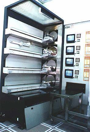
20 Conventional Furnace Equipment 20
21 Thermal Process Hardware Control System Gas Delivery System Loading System Exhaust System Process Tube 21
22 MFC Furnace System MFC MFC MFC Process Tube Control Valve Scrubber Regulator HCl N 2 吹除淨化氮氣 Exhaust Control System 在氧化製程中, 總是把氮氣當作鈍氣應用在系統閒置時 晶圓裝載 溫度提昇 溫度穩定和晶圓卸載等步驟中 乾式氧化步驟中也使用氯化氫,HCl or TCA (trichloroethane), 來減少氧化物中的移動離子, 使其成為不可移動的氯化物化合物, 並將界面電荷 (Interface state charge) 降至最低!! 22
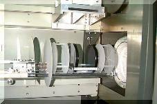
23 Furnace Configuration Horizontal Tube Vertical Tube Center Zone Heating Coils Heaters Gas Flow Quartz Tube T ± 0.5 Flat Zone Tower several hundred wafers Distance Ramp up ~1 /sec 23
24 Dry Oxide Process Sequence Idle with purge N 2 flow Idle with process N 2 flow Wafer boat push in with process N 2 / flow Temperature ramp-up with process N 2 / flow Temperature stabilization with process N 2 / flow Oxidation with, HCl; stop N 2 flow Oxide annealing; stop ; start process N 2 flow Temperature cool-down with process N 2 flow Wafer boat pull out with process N 2 flow Idle with process N 2 flow Repeat process with next boat 24
25 Oxidation Recipe 25
26 Wet Oxidation Faster, higher throughput (H 2 O, HO species) Thick oxide, such as LOCOS Dry oxide has better quality Process Temperature Thickness Oxidation Time Dry oxidation 1000 C 1000 Å ~ 2 hr Wet oxidation 1000 C 1000 Å ~ 12 min Source: Dr. PT Liu 26
27 Effect of Oxidation Ambient Wet oxidation rate is much higher than dry oxidation rate because HO - or H 2 O diffuses much faster than in. 27
28 Pyrogenic Steam System Hydrogen Flame, 2 H H 2 O H 2 To Exhaust Thermal Couple Process Tube Paddle Wafer Boat Typical H 2 : ratio is between 1.8:1 to 1.9:1. 28
")
29 Outside Torch System (OTS) 29
30 Pyrogenic Wet Oxidation System MFC Process Tube MFC MFC MFC Wafers Burn Box Control Valves H 2 Process N 2 Purge N 2 Regulator Scrubbier Exhaust 30
31 Pyrogenic Oxide Process Sequence Idle with purge N 2 flow Idle with process N 2 flow Ramp with process N 2 Wafer boat push in with and process N 2 flows Temperature ramp-up with and process N 2 flows Temperature stabilization with and process N 2 flows Ramp turn off N 2 flow Stabilize flow Turn on H 2 flow, ignition, and H 2 flow stabilization 31
32 Pyrogenic Oxide Process Sequence (Cont.) Steam oxidation with and H 2 flows Hydrogen termination; turn off H 2 while keeping flow Oxygen termination; turn off, start process N 2 flow Temperature ramp-down with process N 2 flow Wafer boat pull out with process N 2 flow Idle with process N 2 flow Repeat process with next boat Idle with purge N 2 flow 32
33 Oxide Measurement Thickness Uniformity SEM, TEM, Profilermeter Color chart Spectrophotometry (Reflectometry) Ellipsometry C-V I-V, breakdown voltage C-V, oxide charge 33
34 Spectrophotometry (Reflectometry) Incident light 1 Interference 2 Human eye or photodetector t Dielectric film, n( λ) Substrate 34

35 Interference in Thin Films 180 o phase change λ 0 n 0 sinφ= n 1 sinβ λ 1 = λ 0 /n 1 n 2 > n 1 > n 0 =1 λ 2nx cosβ 2x cosβ = m λ = n m m = 1,2,3 : constructive interference m = 1/ 2,3 / 2,5 / 2 : distructive interference 35
36 Color Chart 36
37 Spectroreflectometry System Substrate Film Detectors UV lamp Reflectance (%) Constructive interference Destructive interference λ 1 λ 2 λ Wavelength (nm) 37
Chapter 5 Thermal Processes
 Chapter 5 Thermal Processes 1 Topics Introduction Hardware Oxidation Diffusion Annealing Post-Implantation Alloying Reflow High Temp CVD Epi Poly Silicon Nitride RTP RTA RTP Future Trends 2 Definition
Section 4: Thermal Oxidation. Jaeger Chapter 3. EE143 - Ali Javey
 Section 4: Thermal Oxidation Jaeger Chapter 3 Properties of O Thermal O is amorphous. Weight Density =.0 gm/cm 3 Molecular Density =.3E molecules/cm 3 O Crystalline O [Quartz] =.65 gm/cm 3 (1) Excellent
MICROCHIP MANUFACTURING by S. Wolf
 MICROCHIP MANUFACTURING by S. Wolf Chapter 13: THERMAL- OXIDATION of SILICON 2004 by LATTICE PRESS Chapter 13: THERMAL-OXIDATION of SILICON n CHAPTER CONTENTS Applications of Thermal Silicon-Dioxide Physical
CHAPTER 4: Oxidation. Chapter 4 1. Oxidation of silicon is an important process in VLSI. The typical roles of SiO 2 are:
 Chapter 4 1 CHAPTER 4: Oxidation Oxidation of silicon is an important process in VLSI. The typical roles of SiO 2 are: 1. mask against implant or diffusion of dopant into silicon 2. surface passivation
Why silicon? Silicon oxide
 Oxidation Layering. Oxidation layering produces a thin layer of silicon dioxide, or oxide, on the substrate by exposing the wafer to a mixture of highpurity oxygen or water at ca. 1000 C (1800 F). Why
Semiconductor Manufacturing Technology. Semiconductor Manufacturing Technology
 Semiconductor Manufacturing Technology Michael Quirk & Julian Serda October 2001 by Prentice Hall Chapter 10 Oxidation 2001 2000 by Prentice Hall Diffusion Area of Wafer Fabrication Wafer fabrication (front-end)
ELEC 7364 Lecture Notes Summer Si Oxidation. by STELLA W. PANG. from The University of Michigan, Ann Arbor, MI, USA
 ELEC 7364 Lecture Notes Summer 2008 Si Oxidation by STELLA W. PANG from The University of Michigan, Ann Arbor, MI, USA Visiting Professor at The University of Hong Kong The University of Michigan Visiting
Oxide Growth. 1. Introduction
 Oxide Growth 1. Introduction Development of high-quality silicon dioxide (SiO2) has helped to establish the dominance of silicon in the production of commercial integrated circuits. Among all the various
Section 4: Thermal Oxidation. Jaeger Chapter 3
 Section 4: Thermal Oxidation Jaeger Chapter 3 Properties of O Thermal O is amorphous. Weight Density =.0 gm/cm 3 Molecular Density =.3E molecules/cm 3 O Crystalline O [Quartz] =.65 gm/cm 3 (1) Excellent
Doping and Oxidation
 Technische Universität Graz Institute of Solid State Physics Doping and Oxidation Franssila: Chapters 13,14, 15 Peter Hadley Technische Universität Graz Institute of Solid State Physics Doping Add donors
MOSFET. n+ poly Si. p- substrate
 EE143 Midterm #1 Solutions Fall 2005 (maximum score is 97) Problem 1 Processing Modules and Simple Process Sequence (25 points total) The following schematic cross-section shows a MOSFET together with
Semiconductor Technology
 Semiconductor Technology from A to Z Oxidation www.halbleiter.org Contents Contents List of Figures List of Tables II III 1 Oxidation 1 1.1 Overview..................................... 1 1.1.1 Application...............................
More on oxidation. Oxidation systems Measuring oxide thickness Substrate orientation Thin oxides Oxide quality Si/SiO2 interface Hafnium oxide
 More on oxidation Oxidation systems Measuring oxide thickness Substrate orientation Thin oxides Oxide quality Si/SiO2 interface Hafnium oxide EE 432/532 oxide measurements, etc 1 Oxidation systems silicon
Kinetics of Silicon Oxidation in a Rapid Thermal Processor
 Kinetics of Silicon Oxidation in a Rapid Thermal Processor Asad M. Haider, Ph.D. Texas Instruments Dallas, Texas USA Presentation at the National Center of Physics International Spring Week 2010 Islamabad
Oxidation SMT Yau - 1
 Oxidation Yau - 1 Objectives After studying the material in this chapter, you will be able to: 1. Describe an oxide film for semiconductor manufacturing, including its atomic structure, how it is used
EE THERMAL OXIDATION - Chapter 6. Basic Concepts
 EE 22 FALL 999-00 THERMAL OXIDATION - Chapter 6 Basic Concepts SiO 2 and the Si/SiO 2 interface are the principal reasons for silicon s dominance in the IC industry. SiO 2 : Easily selectively etched using
Instructor: Dr. M. Razaghi. Silicon Oxidation
 SILICON OXIDATION Silicon Oxidation Many different kinds of thin films are used to fabricate discrete devices and integrated circuits. Including: Thermal oxides Dielectric layers Polycrystalline silicon
Thermal Oxidation and Growth of Insulators (Chapter 3 - Jaeger 3) Key advantage of Si: Oxidation of Si into SiO 2 (glass) Major factor in making
 Key advantage of Si: Oxidation of Si into SiO 2 (glass) Major factor in making") Thermal Oxidation and Growth of Insulators (Chapter 3 - Jaeger 3) Key advantage of Si: Oxidation of Si into SiO (glass) Major factor in making Silicon the main semiconductor Grown at high temperature in
Thermal Oxidation and Growth of Insulators (Chapter 3 - Jaeger 3) Key advantage of Si: Oxidation of Si into SiO (glass) Major factor in making Silicon the main semiconductor Grown at high temperature in
Processing of Semiconducting Materials Prof. Pallab Banerjee Department of Material Science Indian Institute of Technology, Kharagpur
 Processing of Semiconducting Materials Prof. Pallab Banerjee Department of Material Science Indian Institute of Technology, Kharagpur Lecture - 35 Oxidation I (Refer Slide Time: 00:24) Today s topic of
THERMAL OXIDATION - Chapter 6 Basic Concepts
 THERMAL OXIDATION - Chapter 6 Basic Concepts SiO 2 and the Si/SiO 2 interface are the principal reasons for silicon s dominance in the IC industry. Oxide Thickness µm 0. µm 0 nm nm Thermally Grown Oxides
Silicon Oxides: SiO 2
 Silicon Oxides: SiO 2 Uses: diffusion masks surface passivation gate insulator (MOSFET) isolation, insulation Formation: grown / native thermal: highest quality anodization deposited: C V D, evaporate,
Microelettronica. Planar Technology for Silicon Integrated Circuits Fabrication. 26/02/2017 A. Neviani - Microelettronica
 Microelettronica Planar Technology for Silicon Integrated Circuits Fabrication 26/02/2017 A. Neviani - Microelettronica Introduction Simplified crosssection of an nmosfet and a pmosfet Simplified crosssection
Silicon Wafer Processing PAKAGING AND TEST
 Silicon Wafer Processing PAKAGING AND TEST Parametrical test using test structures regularly distributed in the wafer Wafer die test marking defective dies dies separation die fixing (not marked as defective)
Chapter 4. UEEP2613 Microelectronic Fabrication. Oxidation
 Chapter 4 UEEP2613 Microelectronic Fabrication Oxidation Prepared by Dr. Lim Soo King 24 Jun 2012 Chapter 4...113 Oxidation...113 4.0 Introduction... 113 4.1 Chemistry of Silicon Dioxide Formation... 115
HOMEWORK 4 and 5. March 15, Homework is due on Monday March 30, 2009 in Class. Answer the following questions from the Course Textbook:
 HOMEWORK 4 and 5 March 15, 2009 Homework is due on Monday March 30, 2009 in Class. Chapter 7 Answer the following questions from the Course Textbook: 7.2, 7.3, 7.4, 7.5, 7.6*, 7.7, 7.9*, 7.10*, 7.16, 7.17*,
Chapter 3 CMOS processing technology
 Chapter 3 CMOS processing technology (How to make a CMOS?) Si + impurity acceptors(p-type) donors (n-type) p-type + n-type => pn junction (I-V) 3.1.1 (Wafer) Wafer = A disk of silicon (0.25 mm - 1 mm thick),
Wafer Cleaning and Oxide Growth Laboratory Dr. Lynn Fuller Webpage:
 ROCHESTER INSTITUTE OF TECHNOLOGY MICROELECTRONIC ENGINEERING Wafer Cleaning and Oxide Growth Laboratory Dr. Lynn Fuller Webpage: http://www.rit.edu/~lffeee 82 Lomb Memorial Drive Rochester, NY 14623-5604
the surface of a wafer, usually silicone. In this process, an oxidizing agent diffuses into the wafer
 Analysis of Oxide Thickness Measurement Techniques of SiO2: Nanometrics Nanospec Reflectometer and Color Chart Eman Mousa Alhajji North Carolina State University Department of Materials Science and Engineering
Lecture 4. Oxidation (applies to Si and SiC only) Reading: Chapter 4
 Reading: Chapter 4") Lecture 4 Oxidation (applies to Si and SiC only) Reading: Chapter 4 Introduction discussion: Oxidation: Si (and SiC) Only The ability to grow a high quality thermal oxide has propelled Si into the forefront
Lecture 4 Oxidation (applies to Si and SiC only) Reading: Chapter 4 Introduction discussion: Oxidation: Si (and SiC) Only The ability to grow a high quality thermal oxide has propelled Si into the forefront
EE 143 FINAL EXAM NAME C. Nguyen May 10, Signature:
 INSTRUCTIONS Read all of the instructions and all of the questions before beginning the exam. There are 5 problems on this Final Exam, totaling 143 points. The tentative credit for each part is given to
EE 330 Lecture 9. IC Fabrication Technology Part II. -Oxidation -Epitaxy -Polysilicon -Planarization -Resistance and Capacitance in Interconnects
 EE 330 Lecture 9 IC Fabrication Technology Part II -Oxidation -Epitaxy -Polysilicon -Planarization -Resistance and Capacitance in Interconnects Review from Last Time IC Fabrication Technology Crystal Preparation
EE 330 Lecture 8. IC Fabrication Technology Part II. - Oxidation - Epitaxy - Polysilicon - Interconnects
 EE 330 Lecture 8 IC Fabrication Technology Part II - Oxidation - Epitaxy - Polysilicon - Interconnects Review from Last Time MOS Transistor Bulk Source Gate Drain p-channel MOSFET Lightly-doped n-type
Silicon Epitaxial CVD Want to create very sharp PN boundary grow one type layer on other in single crystal form High dopant layers on low dopant
 Silicon Epitaxial CVD Want to create very sharp PN boundary grow one type layer on other in single crystal form High dopant layers on low dopant substrate Creates latch up protection for CMOS Buried Epi
MOS Gate Dielectrics. Outline
 MOS Gate Dielectrics Outline Scaling issues Technology Reliability of SiO 2 Nitrided SiO 2 High k dielectrics 42 Incorporation of N or F at the Si/SiO 2 Interface Incorporating nitrogen or fluorine instead
VLSI Technology Dr. Nandita Dasgupta Department of Electrical Engineering Indian Institute of Technology, Madras
 VLSI Technology Dr. Nandita Dasgupta Department of Electrical Engineering Indian Institute of Technology, Madras Lecture - 36 MOSFET I Metal gate vs self-aligned poly gate So far, we have discussed about
EE 330 Lecture 9. IC Fabrication Technology Part 2
 EE 330 Lecture 9 IC Fabrication Technology Part 2 Quiz 8 A 2m silicon crystal is cut into wafers using a wire saw. If the wire diameter is 220um and the wafer thickness is 350um, how many wafers will this
Silicon Epitaxial CVD Want to create very sharp PN boundary grow one type layer on other in single crystal form High dopant layers on low dopant
 Silicon Epitaxial CVD Want to create very sharp PN boundary grow one type layer on other in single crystal form High dopant layers on low dopant substrate Creates latch up protection for CMOS Buried Epi
Process Integration. MEMS Release Techniques Sacrificial Layer Removal Substrate Undercut
 Process Integration Self-aligned Techniques LOCOS- self-aligned channel stop Self-aligned Source/Drain Lightly Doped Drain (LDD) Self-aligned silicide (SALICIDE) Self-aligned oxide gap MEMS Release Techniques
University of Texas Arlington Department of Electrical Engineering. Nanotechnology Microelectromechanical Systems Ph.D. Diagnostic Examination
 University of Texas Arlington Department of Electrical Engineering Nanotechnology Microelectromechanical Systems Ph.D. Diagnostic Examination Fall 2012 November 17, 2012 Question # 1 2 3 To be filled by
Chapter 3 Silicon Device Fabrication Technology
 Chapter 3 Silicon Device Fabrication Technology Over 10 15 transistors (or 100,000 for every person in the world) are manufactured every year. VLSI (Very Large Scale Integration) ULSI (Ultra Large Scale
EE40 Lec 22. IC Fabrication Technology. Prof. Nathan Cheung 11/19/2009
 Suggested Reading EE40 Lec 22 IC Fabrication Technology Prof. Nathan Cheung 11/19/2009 300mm Fab Tour http://www-03.ibm.com/technology/manufacturing/technology_tour_300mm_foundry.html Overview of IC Technology
Problem 1 Lab Questions ( 20 points total)
") Problem 1 Lab Questions ( 20 points total) (a) (3 points ) In our EE143 lab, we use Phosphorus for the source and drain diffusion. However, most advanced processes use Arsenic. What is the advantage of
Problem 1 Lab Questions ( 20 points total) (a) (3 points ) In our EE143 lab, we use Phosphorus for the source and drain diffusion. However, most advanced processes use Arsenic. What is the advantage of
EECS130 Integrated Circuit Devices
 EECS130 Integrated Circuit Devices Professor Ali Javey 9/13/2007 Fabrication Technology Lecture 1 Silicon Device Fabrication Technology Over 10 15 transistors (or 100,000 for every person in the world)
Silicon Wafers: Basic unit Silicon Wafers Basic processing unit 100, 150, 200, 300, 450 mm disk, mm thick Current industrial standard 300 mm
 Silicon Wafers: Basic unit Silicon Wafers Basic processing unit 100, 150, 200, 300, 450 mm disk, 0.5-0.8 mm thick Current industrial standard 300 mm (12 inches) Most research labs 100, 150 mm wafers (ours
CMOS Technology. Flow varies with process types & company. Start with substrate selection. N-Well CMOS Twin-Well CMOS STI
 CMOS Technology Flow varies with process types & company N-Well CMOS Twin-Well CMOS STI Start with substrate selection Type: n or p Doping level, resistivity Orientation, 100, or 101, etc Other parameters
Increased Yield Using PDS Products Grade BN-975 with Hydrogen Injection
 Increased Yield Using PDS Products Grade BN-975 with Hydrogen Injection Technical Bulletin The purpose of the hydrogen injection process is to increase die yield per wafer. This is accomplished because
Microelectronics. Integrated circuits. Introduction to the IC technology M.Rencz 11 September, Expected decrease in line width
 Microelectronics Introduction to the IC technology M.Rencz 11 September, 2002 9/16/02 1/37 Integrated circuits Development is controlled by the roadmaps. Self-fulfilling predictions for the tendencies
3.155J / 6.152J Micro/Nano Processing Technology TAKE-HOME QUIZ FALL TERM 2005
 3.155J / 6.152J Micro/Nano Processing Technology TAKE-HOME QUIZ FALL TERM 2005 1) This is an open book, take-home quiz. You are not to consult with other class members or anyone else. You may discuss the
Chapter 5 Thermal Processes
 Chapter 5 Thermal Processes Hong Xiao, Ph. D. hxiao89@hotmail.com Objective List four thermal processes Describe thermal process in IC fabrication Describe thermal oxidation process Explain the advantage
ECE 440 Lecture 27 : Equilibrium P-N Junctions I Class Outline:
 ECE 440 Lecture 27 : Equilibrium P-N Junctions I Class Outline: Fabrication of p-n junctions Contact Potential Things you should know when you leave Key Questions What are the necessary steps to fabricate
Photoresist Coat, Expose and Develop Laboratory Dr. Lynn Fuller
 ROCHESTER INSTITUTE OF TECHNOLOGY MICROELECTRONIC ENGINEERING Photoresist Coat, Expose and Develop Laboratory Dr. Lynn Fuller Webpage: http://www.rit.edu/lffeee 82 Lomb Memorial Drive Rochester, NY 14623-5604
VLSI Digital Systems Design
 VLSI Digital Systems Design CMOS Processing cmpe222_03process_ppt.ppt 1 Si Purification Chemical purification of Si Zone refined Induction furnace Si ingot melted in localized zone Molten zone moved from
Process Integration. NMOS Generic NMOS Process Flow. CMOS - The MOSIS Process Flow
 Process Integration Self-aligned Techniques LOCOS- self-aligned channel stop Self-aligned Source/Drain Lightly Doped Drain (LDD) Self-aligned silicide (SALICIDE) Self-aligned oxide gap MEMS Release Techniques
Oxidation of Silicon
 OpenStax-CNX module: m24908 1 Oxidation of Silicon Andrew R. Barron This work is produced by OpenStax-CNX and licensed under the Creative Commons Attribution License 3.0 note: This module was developed
PDS Products PRODUCT DATA SHEET. BN-975 Wafers. Low Defect Boron Diffusion Systems. Features/Benefits BORON NITRIDE
 Low Defect Boron Diffusion Systems The purpose of the hydrogen injection process is to increase die yield per wafer. This is accomplished because the effects associated with the hydrogen injection process.
Czochralski Crystal Growth
 Czochralski Crystal Growth Crystal Pulling Crystal Ingots Shaping and Polishing 300 mm wafer 1 2 Advantage of larger diameter wafers Wafer area larger Chip area larger 3 4 Large-Diameter Wafer Handling
Chapter 2 Manufacturing Process
 Digital Integrated Circuits A Design Perspective Chapter 2 Manufacturing Process 1 CMOS Process 2 CMOS Process (n-well) Both NMOS and PMOS must be built in the same silicon material. PMOS in n-well NMOS
CHAPTER - 4 CMOS PROCESSING TECHNOLOGY
 CHAPTER - 4 CMOS PROCESSING TECHNOLOGY Samir kamal Spring 2018 4.1 CHAPTER OBJECTIVES 1. Introduce the CMOS designer to the technology that is responsible for the semiconductor devices that might be designed
Isolation Technology. Dr. Lynn Fuller
 ROCHESTER INSTITUTE OF TECHNOLOGY MICROELECTRONIC ENGINEERING Isolation Technology Dr. Lynn Fuller Motorola Professor 82 Lomb Memorial Drive Rochester, NY 14623-5604 Tel (585) 475-2035 Fax (585) 475-5041
Chapter 2 MOS Fabrication Technology
 Chapter 2 MOS Fabrication Technology Abstract This chapter is concerned with the fabrication of metal oxide semiconductor (MOS) technology. Various processes such as wafer fabrication, oxidation, mask
Microstructure of Electronic Materials. Amorphous materials. Single-Crystal Material. Professor N Cheung, U.C. Berkeley
 Microstructure of Electronic Materials Amorphous materials Single-Crystal Material 1 The Si Atom The Si Crystal diamond structure High-performance semiconductor devices require defect-free crystals 2 Crystallographic
Fabrication Technology
 Fabrication Technology By B.G.Balagangadhar Department of Electronics and Communication Ghousia College of Engineering, Ramanagaram 1 OUTLINE Introduction Why Silicon The purity of Silicon Czochralski
This Appendix discusses the main IC fabrication processes.
 IC Fabrication B B.1 Introduction This Appendix discusses the main IC fabrication processes. B.2 NMOS fabrication NMOS transistors are formed in a p-type substrate. The NMOS fabrication process requires
A discussion of crystal growth, lithography, etching, doping, and device structures is presented in
 Chapter 5 PROCESSING OF DEVICES A discussion of crystal growth, lithography, etching, doping, and device structures is presented in the following overview gures. SEMICONDUCTOR DEVICE PROCESSING: AN OVERVIEW
Etching Etching Definitions Isotropic Etching: same in all direction Anisotropic Etching: direction sensitive Selectivity: etch rate difference
 Etching Etching Definitions Isotropic Etching: same in all direction Anisotropic Etching: direction sensitive Selectivity: etch rate difference between 2 materials Need strong selectivity from masking
Lecture 030 Integrated Circuit Technology - I (5/8/03) Page 030-1
 Page 030-1") Lecture 030 Integrated Circuit Technology - I (5/8/03) Page 030-1 LECTURE 030 INTEGRATED CIRCUIT TECHNOLOGY - I (References [7,8]) Objective The objective of this presentation is: 1.) Illustrate integrated
Lecture 030 Integrated Circuit Technology - I (5/8/03) Page 030-1 LECTURE 030 INTEGRATED CIRCUIT TECHNOLOGY - I (References [7,8]) Objective The objective of this presentation is: 1.) Illustrate integrated
ME 141B: The MEMS Class Introduction to MEMS and MEMS Design. Sumita Pennathur UCSB
 ME 141B: The MEMS Class Introduction to MEMS and MEMS Design Sumita Pennathur UCSB Outline today Introduction to thin films Oxidation Deal-grove model CVD Epitaxy Electrodeposition 10/6/10 2/45 Creating
VLSI INTRODUCTION P.VIDYA SAGAR ( ASSOCIATE PROFESSOR) Department of Electronics and Communication Engineering, VBIT
 Department of Electronics and Communication Engineering, VBIT") VLSI INTRODUCTION P.VIDYA SAGAR ( ASSOCIATE PROFESSOR) contents UNIT I INTRODUCTION: Introduction to IC Technology MOS, PMOS, NMOS, CMOS & BiCMOS technologies. BASIC ELECTRICAL PROPERTIES : Basic Electrical
VLSI INTRODUCTION P.VIDYA SAGAR ( ASSOCIATE PROFESSOR) contents UNIT I INTRODUCTION: Introduction to IC Technology MOS, PMOS, NMOS, CMOS & BiCMOS technologies. BASIC ELECTRICAL PROPERTIES : Basic Electrical
Fairchild Semiconductor Application Note June 1983 Revised March 2003
 Fairchild Semiconductor Application Note June 1983 Revised March 2003 High-Speed CMOS (MM74HC) Processing The MM74HC logic family achieves its high speed by utilizing microcmos Technology. This is a 3.5
Lecture 0: Introduction
 Lecture 0: Introduction Introduction Integrated circuits: many transistors on one chip. Very Large Scale Integration (VLSI): bucketloads! Complementary Metal Oxide Semiconductor Fast, cheap, low power
State of the art quality of a GeOx interfacial passivation layer formed on Ge(001)
") APPLICATION NOTE State of the art quality of a Ox interfacial passivation layer formed on (001) Summary A number of research efforts have been made to realize Metal-Oxide-Semiconductor Field Effect Transistors
APPLICATION NOTE State of the art quality of a Ox interfacial passivation layer formed on (001) Summary A number of research efforts have been made to realize Metal-Oxide-Semiconductor Field Effect Transistors
Passivation of SiO 2 /Si Interfaces Using High-Pressure-H 2 O-Vapor Heating
 Jpn. J. Appl. Phys. Vol. 39 (2000) pp. 2492 2496 Part, No. 5A, May 2000 c 2000 The Japan Society of Applied Physics Passivation of O 2 / Interfaces Using High-Pressure-H 2 O-Vapor Heating Keiji SAKAMOTO
PROCESS FLOW AN INSIGHT INTO CMOS FABRICATION PROCESS
 Contents: VI Sem ECE 06EC63: Analog and Mixed Mode VLSI Design PROCESS FLOW AN INSIGHT INTO CMOS FABRICATION PROCESS 1. Introduction 2. CMOS Fabrication 3. Simplified View of Fabrication Process 3.1 Alternative
CS/ECE 5710/6710. N-type Transistor. N-type from the top. Diffusion Mask. Polysilicon Mask. CMOS Processing
 CS/ECE 5710/6710 CMOS Processing Addison-Wesley N-type Transistor D G +Vgs + Vds S N-type from the top i electrons - Diffusion Mask Mask for just the diffused regions Top view shows patterns that make
Figure 2.3 (cont., p. 60) (e) Block diagram of Pentium 4 processor with 42 million transistors (2000). [Courtesy Intel Corporation.
 (e) Block diagram of Pentium 4 processor with 42 million transistors (2000). [Courtesy Intel Corporation.") Figure 2.1 (p. 58) Basic fabrication steps in the silicon planar process: (a) oxide formation, (b) selective oxide removal, (c) deposition of dopant atoms on wafer, (d) diffusion of dopant atoms into exposed
Figure 2.1 (p. 58) Basic fabrication steps in the silicon planar process: (a) oxide formation, (b) selective oxide removal, (c) deposition of dopant atoms on wafer, (d) diffusion of dopant atoms into exposed
CMOS FABRICATION. n WELL PROCESS
 CMOS FABRICATION n WELL PROCESS Step 1: Si Substrate Start with p- type substrate p substrate Step 2: Oxidation Exposing to high-purity oxygen and hydrogen at approx. 1000 o C in oxidation furnace SiO
Lecture 22: Integrated circuit fabrication
 Lecture 22: Integrated circuit fabrication Contents 1 Introduction 1 2 Layering 4 3 Patterning 7 4 Doping 8 4.1 Thermal diffusion......................... 10 4.2 Ion implantation.........................
Amorphous and Polycrystalline Thin-Film Transistors
 Part I Amorphous and Polycrystalline Thin-Film Transistors HYBRID AMORPHOUS AND POLYCRYSTALLINE SILICON DEVICES FOR LARGE-AREA ELECTRONICS P. Mei, J. B. Boyce, D. K. Fork, G. Anderson, J. Ho, J. Lu, Xerox
Materials Characterization
 Materials Characterization C. R. Abernathy, B. Gila, K. Jones Cathodoluminescence (CL) system FEI Nova NanoSEM (FEG source) with: EDAX Apollo silicon drift detector (TE cooled) Gatan MonoCL3+ FEI SEM arrived
Department of Electrical Engineering. Jungli, Taiwan
 Chapter 3 Fabrication of CMOS Integrated Circuits Jin-Fu Li Department of Electrical Engineering National Central University Jungli, Taiwan Background Outline The CMOS Process Flow Design Rules Latchup
X-Ray Reflectivity Study of Hafnium Silicate Thin Films Prepared by Thermal Chemical Vapor Deposition
 X-Ray Reflectivity Study of Hafnium Silicate Thin Films Prepared by Thermal Chemical Vapor Deposition Hideyuki YAMAZAKI, Advanced LSI Technology Laboratory, Toshiba Corporation hideyuki.yamazaki@toshiba.co.jp
行政院國家科學委員會補助專題研究計畫成果報告
 NSC89-2215-E-009-104 89 08 01 90 07 31 Fabrication and Characterization of Low-Temperature Polysilicon Thin Film Transistors with Novel Self-Aligned Sub-Gate Structures NSC89-2215-E009-104 (FID) self-aligned
Rapid Thermal Processing (RTP) Dr. Lynn Fuller
 Dr. Lynn Fuller") ROCHESTER INSTITUTE OF TECHNOLOGY MICROELECTRONIC ENGINEERING Rapid Thermal Processing (RTP) Dr. Lynn Fuller Webpage: http://people.rit.edu/lffeee 82 Lomb Memorial Drive Rochester, NY 14623-5604 Tel (585)
ROCHESTER INSTITUTE OF TECHNOLOGY MICROELECTRONIC ENGINEERING Rapid Thermal Processing (RTP) Dr. Lynn Fuller Webpage: http://people.rit.edu/lffeee 82 Lomb Memorial Drive Rochester, NY 14623-5604 Tel (585)
Bruce Furnace Recipes Dr. Lynn Fuller Webpage: Electrical and Microelectronic Engineering
 ROCHESTER INSTITUTE OF TECHNOLOGY MICROELECTRONIC ENGINEERING Bruce Furnace Recipes Dr. Lynn Fuller Webpage: http://people.rit.edu/lffeee Electrical and 82 Lomb Memorial Drive Rochester, NY 14623-5604
Ion Implantation Most modern devices doped using ion implanters Ionize gas sources (single +, 2+ or 3+ ionization) Accelerate dopant ions to very
 Accelerate dopant ions to very") Ion Implantation Most modern devices doped using ion implanters Ionize gas sources (single +, 2+ or 3+ ionization) Accelerate dopant ions to very high voltages (10-600 KeV) Use analyzer to selection charge/mass
Ion Implantation Most modern devices doped using ion implanters Ionize gas sources (single +, 2+ or 3+ ionization) Accelerate dopant ions to very high voltages (10-600 KeV) Use analyzer to selection charge/mass
FABRICATION of MOSFETs
 FABRICATION of MOSFETs CMOS fabrication sequence -p-type silicon substrate wafer -creation of n-well regions for pmos transistors, -impurity implantation into the substrate. -thick oxide is grown in the
EE 5344 Introduction to MEMS. CHAPTER 3 Conventional Si Processing
 3. Conventional licon Processing Micromachining, Microfabrication. EE 5344 Introduction to MEMS CHAPTER 3 Conventional Processing Why silicon? Abundant, cheap, easy to process. licon planar Integrated
Development of High Voltage Silicon Carbide MOSFET Devices in KERI
 Development of High Voltage Silicon Carbide MOSFET Devices in KERI 2014. 06. Kim, Sang Cheol (sckim@keri.re.kr) Power Semiconductor Device Research Center Korea Electrotechnology Research Institute Contents
Lecture 200 BiCMOS Technology (12/12/01) Page 200-1
 Page 200-1") Lecture 200 BiCMOS Technology (12/12/01) Page 200-1 LECTURE 200 BICMOS TECHNOLOGY (READING: Text-Sec. 2.11) INTRODUCTION Objective Illustrate BiCMOS technology Outline Introduction Physical process illustration
Lecture 200 BiCMOS Technology (12/12/01) Page 200-1 LECTURE 200 BICMOS TECHNOLOGY (READING: Text-Sec. 2.11) INTRODUCTION Objective Illustrate BiCMOS technology Outline Introduction Physical process illustration
MOLYBDENUM AS A GATE ELECTRODE FOR DEEP SUB-MICRON CMOS TECHNOLOGY
 Mat. Res. Soc. Symp. Vol. 611 2000 Materials Research Society MOLYBDENUM AS A GATE ELECTRODE FOR DEEP SUB-MICRON CMOS TECHNOLOGY Pushkar Ranade, Yee-Chia Yeo, Qiang Lu, Hideki Takeuchi, Tsu-Jae King, Chenming
Fabrication and Layout
 ECEN454 Digital Integrated Circuit Design Fabrication and Layout ECEN 454 3.1 A Glimpse at MOS Device Polysilicon Aluminum ECEN 475 4.2 1 Material Classification Insulators Glass, diamond, silicon oxide
CMOS VLSI Design. Introduction. All materials are from the textbook Weste and Harris, 3 rd Edition CMOS VLSI DESIGN. Introduction
 CMOS VLSI Design Introduction ll materials are from the textbook Weste and Harris, 3 rd Edition CMOS VLSI DESIGN Introduction Chapter previews the entire field, subsequent chapters elaborate on specific
A Novel Low Temperature Self-Aligned Field Induced Drain Polycrystalline Silicon Thin Film Transistor by Using Selective Side-Etching Process
 Chapter 3 A Novel Low Temperature Self-Aligned Field Induced Drain Polycrystalline Silicon Thin Film Transistor by Using Selective Side-Etching Process 3.1 Introduction Low-temperature poly-si (LTPS) TFTs
Physical Vapor Deposition (PVD) Zheng Yang
 Zheng Yang") Physical Vapor Deposition (PVD) Zheng Yang ERF 3017, email: yangzhen@uic.edu Page 1 Major Fabrication Steps in MOS Process Flow UV light Mask oxygen Silicon dioxide photoresist exposed photoresist oxide
Physical Vapor Deposition (PVD) Zheng Yang ERF 3017, email: yangzhen@uic.edu Page 1 Major Fabrication Steps in MOS Process Flow UV light Mask oxygen Silicon dioxide photoresist exposed photoresist oxide
VLSI Technology Dr. Nandita Dasgupta Department of Electrical Engineering Indian Institute of Technology, Madras
 VLSI Technology Dr. Nandita Dasgupta Department of Electrical Engineering Indian Institute of Technology, Madras Lecture - 33 Problems in LOCOS + Trench Isolation and Selective Epitaxy So, we are discussing
Microfabrication of Integrated Circuits
 Microfabrication of Integrated Circuits OUTLINE History Basic Processes Implant; Oxidation; Photolithography; Masks Layout and Process Flow Device Cross Section Evolution Lecture 38, 12/05/05 Reading This
Edinburgh Microfabrication Facility, University of Edinburgh.
 405 CONTROL OF OXIDE GROWTH BY REAL-TIME SIMULATION E. Cameron, J. Robertson, R. Holwill Edinburgh Microfabrication Facility, University of Edinburgh. SUMMARY As critical device features are reduced in
3.155J / 6.152J MICROELECTRONICS PROCESSING TECHNOLOGY TAKE-HOME QUIZ FALL TERM 2003
 3.155J / 6.152J MICROELECTRONICS PROCESSING TECHNOLOGY TAKE-HOME QUIZ FALL TERM 2003 1) This is an open book, take-home quiz. You are not to consult with other class members or anyone else. You may discuss
Semiconductor Manufacturing Technology. IC Fabrication Process Overview
 Semiconductor Manufacturing Technology Michael Quirk & Julian Serda October 00 by Prentice Hall Chapter 9 IC Fabrication Process Overview /4 Objectives After studying the material in this chapter, you