DESIGN FOR MECHANICAL RELIABILITY OF REDISTRIBUTION LAYERS FOR ULTRA-THIN 2.5D GLASS PACKAGES
|
|
|
- Eileen Owens
- 6 years ago
- Views:
Transcription
1 DESIGN FOR MECHANICAL RELIABILITY OF REDISTRIBUTION LAYERS FOR ULTRA-THIN 2.5D GLASS PACKAGES A Dissertation Presented to The Academic Faculty by Scott McCann In Partial Fulfillment of the Requirements for the Degree Doctor of Philosophy in the George W. Woodruff School of Mechanical Engineering Georgia Institute of Technology May 2017 COPYRIGHT 2017 BY SCOTT R. MCCANN
2 DESIGN FOR MECHANICAL RELIABILITY OF REDISTRIBUTION LAYERS FOR ULTRA-THIN 2.5D GLASS PACKAGES Approved by: Dr. Suresh K. Sitaraman, Advisor School of Mechanical Engineering Georgia Institute of Technology Dr. Rao R. Tummala School of Electrical & Computer Engineering Georgia Institute of Technology Dr. I Charles Ume School of Mechanical Engineering Georgia Institute of Technology Dr. Venkatesh Sundaram School of Electrical & Computer Engineering Georgia Institute of Technology Dr. Shuman Xia School of Mechanical Engineering Georgia Institute of Technology Date Approved: March 20, 2017
3 To my parents
4 ACKNOWLEDGEMENTS Throughout my life and during my time at Georgia Tech, so many people have offered their time and effort to help me along the way. There are far more people I am thankful to or near as much thanks to express how grateful I am than I have space for here. I have sincere gratitude to my advisor, Dr. Suresh K. Sitaraman, for his guidance and steady support during my years at Georgia Tech. The consistency with which he operates, even under high pressure, is always appreciated. I am very grateful for his immense patience throughout my graduate work, especially in my early graduate years. While challenging for me, he helped me grow in leadership, cognizance, and inquisitiveness, and those lessons will stay with me throughout my life. I would like to thank Dr. I. Charles Ume and Dr. Shuman Xia for serving as members on my committee and offering valuable insight on my work. I would like to offer my sincerest thanks to Dr. Rao R. Tummala for his remarkable long term vision and guidance of the 3D Packaging Research Center and to Dr. Venkatesh Sundaram for his daily industry interaction. I am extremely grateful to both Dr. Tummala and Dr. Sundaram, as they are responsible for the motivation for my work. In addition, I would like to thank the 3D Packaging Research Center industry consortium, which funded this research. I am particularly grateful to Dr. Frank Wei, Ichiro Satou, Dr. Aric Shorey, Dr. Hobie Yun, Robin Taylor, Dr. Tobias Bernhard, and Dr. Frank Von-Horsten for their collaboration. iv
5 I am extremely grateful to all the students, interns, visiting engineers, support staff, and others that have helped me during my time graduate studies. Thank you to Sathyanarayanan Raghavan, Makoto Kobayashi, Laura Wambera, Christine Taylor, Yutaka Takagi, David Samet, Tomo Ogawa, Justin Chow, Bhupender Singh, Ting-Chia Nathan Huang, Jialing Tong, Yuya Suzuki, Xian Qin, Wei Chen, Raphael Okereke, Greg Ostrowicki, Abhishek Kwatra, Yeming Paula Xian, V.N.N. Trilochan, Jose Soler, Ninad Shahane, Vidya Jayaram, Tim Huang, Brett Sawyer, Zihan Wu, Ryuta Furuya, Hao Lu, Gary Menezes, Anh Tran, Dr. M. Raj Pulugurtha, Dr. Himani Sharma, Dr. Kadappan Panayappan, Karen May, Patricia Allen, Christa Ernst, Brian McGlade, Chris White, Jason Bishop, the rest of the CASPaR lab members, and the rest of the 3D Packaging Research Center students and interns for their help with modeling, help with experiments, organization, mentoring, and friendship. And to my good friends, David Casey Woodrum, Bruce Chou, Sir Ahmad Humyn, Grace Chen, Arri Hana, Matthew Blacksen Enthoven, Barbara Keytar Smith, Daniel Songo Yune, Kenneth Zhu, and Ryan Lawson, who help keep me sane and remind me that there s life outside work. And to Dr. Vanessa Smet for her help, mentoring, and friendship. I would like to thank my parents, who have been an unbelievably stable, positive guidance throughout my life and who have helped me to grow and been there through the good times and bad times. I would especially like to thank my sister for friendship and tolerance, my Dad, David McCann, for his caring and teaching, and my Mom, Barb McCann, for her incredible patience and love. I cannot imagine a better role model than my Dad. And my Mom s love has always been more amazing than I will ever be able to comprehend. v
6 TABLE OF CONTENTS ACKNOWLEDGEMENTS LIST OF TABLES LIST OF FIGURES LIST OF SYMBOLS AND ABBREVIATIONS SUMMARY iv ix xii xxi xxvi CHAPTER 1. INTRODUCTION Strategic Need for Advanced Packaging Introduction to 2.5D Packaging Need for a Glass Package State-of-the-Art Ultra-thin 2.5D Glass Packages Technical Challenges for Ultra-thin 2.5D Glass Packages Glass Cracking Interfacial Debonding of Redistribution Layers 14 CHAPTER 2. LITERATURE REVIEW Brittle Fracture Mechanics Dicing-induced Defects Free-edge Effect and Glass Stresses Due to Redistribution Layers Glass Strengthening Mechanisms Thin Film Adhesion and Interfacial Debonding Electrical Considerations for Interposer Design 35 CHAPTER 3. OBJECTIVES AND APPROACH 41 CHAPTER 4. SUBSTRATE FABRICATION PROCESS 44 CHAPTER 5. DICING PROCESES AND DICING-INDUCED DEFECTS Blade Dicing of Ultra-thin Glass Laser Dicing of Ultra-thin Glass Dicing Methods Comparison 59 CHAPTER 6. REDISTRUBTION LAYER-INDUCED STRESSES Stress Measurement Through Birefringence Experimental Fabrication Birefringence Measurements Model Correlation Model Validation Through Shadow Moiré Warpage Measurements Shadow Moiré Warpage Measurements Warpage Prediction and Validation 74 vi
7 CHAPTER 7. PREDICTING CRACK PROPAGATION IN GLASS SUBSTRATES Initial Experimental Data Numerical Modeling of Glass Cracking Model to Simulate Blade Dicing Model to Simulate Thermal Cycling Dicing Optimization and Thinner Stack Up Experiments 95 CHAPTER 8. PREVENTING GLASS CRACKING DUE TO DICING- INDUCED DEFECTS AND REDISRIBUTION LAYER STRESSES Demonstration of Glass Cracking Prevention Adhesion Improvement and Solution Demonstration Using Non-epoxy Low Loss Polymer Solution Demonstration Using ABF GX Design Guidelines Model Calibration Design Guideline Recommendations for Glass Cracking 108 CHAPTER 9. PROCESS INNOVATIONS TO PREVENT GLASS CRACKING Edge Coating Fabrication Process for Edge Coating Modeling of Edge Coating Experimental Results for Edge Coating Edge Coating Discussion Two-step Dicing Process for Two-step Dicing Modeling of Two-step Dicing Experimental Results for Two-step Dicing Laser Dicing Process for CO2 Laser Ablation Dicing Experimental Results for CO2 Laser Ablation Dicing CO2 Laser Ablation Dicing Discussion 129 CHAPTER 10. REDISTRIBTION LAYER RELIABILITY AND ADHESION OF COPPER LINES Sequential Crack Extension Method Example Sequential Crack Extension for 90-Degree Peel Test Sequential Crack Extension Discussion Redistribution Layer Adhesion Discussion 148 CHAPTER 11. CONCLUSIONS, CONTRIBUTIONS, AND OUTLOOK Conclusions Contributions Future Work 154 APPENDIX I. MATERIAL MODELS 156 vii
8 APPENDIX II. EXAMPLE RAW DATA OF THERMAL CYCLING RELIABILITY FOR GLASS SUBSTRATES 160 REFERENCES 173 viii
9 LIST OF TABLES Table 1 Comparison of substrate core material options (adapted from [9])... 5 Table 2 2.5D substrate packaging metrics and state of the art Table 3 Electrical design targets for 2.5D interposer up to GHz (credit: [133]). 37 Table 4 Two-dimensional line specifications for 50 Ω impedance matching for nonepoxy low loss (NELL) polymer and ABF GX-92 (credit: [133]) Table 5 Challenges and tasks for RDL reliability of 2.5D ultra-thin glass substrates.. 43 Table 6 Substrate fabrication process details Table 7 Design of experiments for optimizing blade dicing of ultra-thin glass (adapted from [53]) Table 8 Optimized process parameters for blade dicing glass Table 9 Comparison of dicing methods for ultra-thin glass panels Table 10 List of samples fabricated with ABF GX Table 11 Details for Sample Batch Table 12 Batch 1 experimental results from fabrication, dicing, preconditioning, and temperature cycling Table 13 Comparison of energy release rates from models during and after dicing Table 14 Details for Sample Batches 2a and 2b Table 15 Sample Batches 2a and 2b experimental results from fabrication, dicing, preconditioning, and temperature cycling Table 16 Details for Sample Batches 3a and 3b (all dimensions are in μm) ix
10 Table 17 Sample Batches 3a and 3b experimental results from fabrication, dicing, preconditioning, and temperature cycling Table 18 Thermal cycling reliability results for ABF GX Table 19 Details for edge coated samples Table 20 Experimental results from fabrication, dicing, and temperature cycling for edge coating Table 21 Details for two-step laser ablation diced samples Table 22 Experimental results from fabrication, dicing, and temperature cycling for two-step dicing Table 23 Details for CO2 laser ablation diced samples Table 24 Experimental results from fabrication, dicing, and temperature cycling for laser ablation dicing Table 25 Experimental results from fabrication, dicing, and temperature cycling for laser ablation dicing and edge coating Table 26 EN-A1 Glass from Asahi Glass Co., Ltd. material properties [159] Table 27 SWG3 Glass from Corning Inc. material properties Table 28 CF-XX from Asahi Glass Co., Ltd material properties Table 29 Copper material properties (elastic regime) Table 30 Non-epoxy low loss material properties [162] Table 31 Ajinomoto Build-up Film (ABF) GX-92 material properties [28] Table 32 Hitachi s FZ-2700GA solder resist passivation material properties [163] Table 33 NAMICS XWUF edge coating material properties Table 34 Silicon material properties [164] x
11 Table Sn-3.5Ag solder material properties base [165] Table Sn-3.5Ag solder constants for Anand s model for viscoplasticity [160, 165] xi
12 LIST OF FIGURES Figure 1 (a) Individual package layout, (b) system-on-chip (SoC) package, and (c) multi-chip module (MCM) or system-in-package (SiP) (credit: [2])... 2 Figure 2 (a) 2D IC, (b) 2.5D, and (c) 3D IC (credit: [2])... 2 Figure 3 Comparison of 3D IC packages (credit: [5]) Figure 4 AMD s Radeon TM Fury GPU showing (a) overhead view of package, (b) cross section of package, and (c) SEM of die region (credit: [6])... 4 Figure 5 Cross section schematic of ultra-thin 2.5D glass interposer Figure 6 (a) Illustration of 2.5D glass package cracking technical challenge, (b) 2.5D glass substrates cracking immediately after dicing, and (c) acoustic microgrpah of 2.5D glass substrates cracking during thermal cycle reliability testing Figure 7 Copper peeling from bare glass (credit: Bernhard) Figure 8 Two-dimensional crack tip coordinate system and plastic zone (shape not to scale) Figure 9 Two-dimensional crack tip and J integral contour Figure 10 (a) Mode I opening fracture, (b) mode II in-plane shearing fracture, and (c) mode III out-of-plane shearing fracture Figure 11 Stress intensity factor tests (credit: [61, 65]) Figure 12 (a) Ring-on-ring test schematic (credit: [82]) and (b) two point bend test schematic (credit: [83]) xii
13 Figure 13 Critical stress intensity factor for different types of glasses in water (credit: [86, 88]) Figure 14 Crack propagation velocity as a function of stress intensity factor for sodalime glass in air with varying moisture content (credit: [89, 90]) Figure 15 (a) σz along center of top layer (z = (3/2)h), (b) τxy along center of top layer (z = (3/2)h), (c) σz along 0/90 interface (z = h), (d) τxy along 45/-45 interface (z = h) (credit: [99]) Figure 16 A polarized wave passing through a medium, showing phase retardation (credit: Mellish) Figure 17 (a) Before and (b) after ion exchange process (credit: Corning, Inc.) Figure 18 Temperature profile for annealing glass (credit: GOEL Process Systems Pvt. Ltd.) Figure 19 Interfacial adhesion strength tests (credit: [124]) Figure 20 Three-dimensional analysis of two fan-out routing patterns for 50 Ω impedance matching, (a) die escape line matched and (b) die-to-die fanout matched (credit: [133]) Figure 21 Three-dimensional EM analysis of return loss (credit: [133]) Figure 22 Three-dimensional EM analysis of insertion loss (credit: [133]) Figure 23 Build-up thickness illustration from electrical design for 2.5D interposer with 128 GB/s in a 10.0 mm wide bus Figure 24 Fabrication process sequence for glass panel Figure 25 Example mask set for 2.5D glass interposer (credit: [133]) xiii
14 Figure µm thick glass panel after fabrication, showing (a) the entire panel, (b) a full glass interposer prior to singulation, (c) passivation surface finish opening alignment and (d) close-up of passivation surface finish opening (credit: [133]) Figure 27 (a) 100 µm thick glass panel after fabrication with coupon ID and (b) glass interposer with test structure identification (credit: [133]) Figure 28 Optical micrograph of a glass edge after dicing Figure 29 Glass sidewall line roughness, Ra, as a function of diamond grit size for blade dicing (adapted from [53]) Figure 30 Summary of glass sidewall roughness, Ra, from Table 27 (adapted from [53]) Figure 31 Glass substrate edge after CO2 laser ablation dicing Figure 32 Cross section of CO2 laser ablation diced sample Figure 33 Three glass coupons after singulation, showing B with no copper (left), C with 75% copper (center), and C with 50% copper (right). Scale is in cm.. 63 Figure 34 Sample preparation and birefringence measurement process Figure 35 Stress contour measured through birefringence for an F (50%) sample (300 µm glass coupon with 34 µm polymer and 10 µm copper) Figure 36 Comparison of the difference in secondary principal stresses along the white line in Figure 35 as measured through birefringence and predicted through modeling (part 1/2) xiv
15 Figure 37 Comparison of the difference in secondary principal stresses along the white line in Figure 35 as measured through birefringence and predicted through modeling (part 2/2) Figure 38 Finite-element model geometry and mesh for birefringence comparison Figure 39 Cross section schematic of a glass ball grid array package for smart mobile application Figure 40 Tool head temperature and pressure profile used for thermo-compression bonding. The stage is held at 70 C throughout the process Figure 41 Silicon die assembled on a four-metal-layer glass substrate with B-staged underfill Figure 42 Glass package at room temperature (die region shadow moiré measurement from die side) showing 8 μm warpage Figure 43 Comparison of experimentally measured and model predicted die warpage for a glass package Figure 44 Example plane-strain model for the Low-CTE Glass Sample Figure 45 Fabrication and assembly process temperature sequence used in birth and death modeling Figure 46 Optical inspection of glass substrate edge to show failure classification: (a) pock marks after dicing (green), (b) interfacial delamination between glass and polymer (orange), and (c) cracking of glass substrate after interfacial failure (red) Figure 47 Experimental classification scheme xv
16 Figure 48 (a) Schematic of four metal layer glass substrate and (b) overhead optical image after fabrication and dicing Figure 49 Cohesive cracking of glass substrate Figure 50 SEM of glass substrate edge after crack propagation, showing dicing-induced defects, delamination, and cohesive cracking of the glass Figure 51 SEM of glass substrate corner after crack propagation, showing delamination of glass-polymer interface Figure 52 Finite element model geometry schematic Figure 53 (a) Example of finite element model mesh near free edge and (b) close-up of crack tip (contour integral shown) Figure 54 Finite element geometry for model simulating dicing Figure 55 Energy release rate as a function of initial defect size during dicing for a cohesive crack in the glass substrate 15 μm from the glass-polymer interface simulating dicing Figure 56 Energy release rate at -40 C as a function of initial defect size for cohesive cracking of a glass substrate simulating thermal cycling reliability Figure 57 Schematic of cracking from glass-polymer interface into glass Figure 58 Energy release rate at -40 C as a function of initial delamination size for a crack kinking into the glass substrate simulating thermal cycling reliability Figure 59 Schematic of solder resist pullback. Pullback distance is measured from the edge of the dicing street xvi
17 Figure 60 Effect of passivation pullback and full pullback on energy release rate during dicing Figure 61 (a) CSAM and (b) optical inspection of corners of Sample 3b-F2 after 1000 temperature cycles Figure 62 Energy release rate for each sample structure. Samples above the red line are predicted to crack while samples below the green line are predicted not to crack. Numbers above columns summarize thermal cycling results through 1000 cycles Figure 63 Design guideline to prevent glass cracking due to RDL stresses and dicinginduced defects. The guidelines apply for 100 µm thick 2.5D glass interposer using ABF GX Figure 64 Design guideline to prevent glass cracking due to RDL stresses and dicinginduced defects. The guidelines apply for 100 µm thick 2.5D glass interposer using non-epoxy low loss polymer Figure 65 Finite element model for edge coated substrate Figure 66 Cross section of edge coated sample which had a crack before edge coating was applied Figure 67 Out-of-plane stress in the glass for samples (a) without edge coating and (b) with edge coating for a 100 μm crack (deformation is 5x exaggerated) Figure 68 Energy release rate at -40 C as a function of initial crack size for substrates with and without edge coating Figure 69 Two-step diced sample from the top Figure 70 Finite element model for two-step dicing xvii
18 Figure 71 Cross section of two-step diced sample Figure 72 Design rule map for required pullback length to prevent glass cracking for blade dicing Figure 73 Schematic for sequential crack extension. Nodes within green boxes are coupled Figure 74 Peel strength of 10 µm electroplated copper on borosilicate glass (credit: [150]) Figure 75 Domain for 2D plane-strain analysis of 90-degree peel test under constant applied load Figure 76 Stress-strain relationship for the copper thin film Figure 77 Analysis domain and example finite-element mesh regions Figure 78 The total accumualted equivalent plastic strain in the copper thin film for P/b = 3.0 N/cm Figure 79 The accumulated plastic strain in the copper thin film over one cycle accumulated over one cycle showing where the plastic deformation occurs for P/b = 3.0 N/cm Figure 80 External work, elastic strain, and plastic strain energy rates as the crack propagates from an initial crack length, anom = 100 μm, under a peel force of P/b = 3.0 N/cm for a 10 μm thick film. Crack growth through regions A, B, C, and D correspond to element size, δa, of 2, 1, 0.5, and 0.25 μm, respectively Figure 81 Steady state energy release rate as a function of mesh density xviii
19 Figure 82 (a) Tangential, (b) normal, and (c) shear stress fields near crack tip during steady-state peeling for P/b = 3.0 N/cm for a 10 μm film Figure 83 Strain energy release rate calculated through SCE and VCCT as the crack propagates from an initial crack length, anom = 100 μm, under a peel force of P/b = 3.0 N/cm for a 10 μm thick film. Crack growth through regions A, B, C, and D correspond to element size, δa, of 2, 1, 0.5, and 0.25 μm, respectively Figure 84 External work, elastic strain, and plastic strain energy rates as the crack propagates, and subsequently moving the peel force location beyond the initial crack length (region B2) Figure 85 Relationship between critical strain energy release rate and peel force for a 10 µm electroplated copper film on a borosilicate glass substrate Figure 86 CTE of EN-A1 glass [159] Figure 87 Batch 1 (NELL polymer) Sample E3 after 1000 thermal cycles Figure 88 Batch 2a (NELL polymer) Sample C3 after 1000 thermal cycles Figure 89 Batch 2a (NELL polymer) sample with high CTE glass after 1000 thermal cycles Figure 90 Batch 2b (NELL polymer) Sample E5 after 1000 thermal cycles Figure 91 Two-step dicing (NELL polymer) Sample E4 after 1000 thermal cycles Figure 92 Batch 3a (NELL polymer) Sample F1 after 1000 thermal cycles Figure 93 Batch 3b (NELL polymer) Sample F2 after 1000 thermal cycles Figure 94 Sample A-2b (ABF GX-92) at t Figure 95 Sample A-2b (ABF GX-92) after 1000 thermal cycles xix
20 Figure 96 Sample C2-R (50%) (ABF GX-92) after 1000 thermal cycles Figure 97 Sample D2-R (75%) (ABF GX-92) after 1000 thermal cycles Figure 98 Sample F2-L (75%) (ABF GX-92) after 50 thermal cycles Figure 99 Sample E1-L (50%) (ABF GX-92) after 250 thermal cycles xx
21 LIST OF SYMBOLS AND ABBREVIATIONS 2D Two-dimensional 2.5D Two-and-a-half dimensional 3D Three-dimensional A Area AA Pre-exponential factor in Anand s viscoplasticity da Incremental area a Crack length aa Strain rate sensitivity of hardening or softening in Anand s viscoplasticity b Width bv Hardening parameter for nonlinear isotropic hardening Voce power law C4 Controlled collapse chip connection CoWoS Chip-on-Wafer-on-Substrate CSAM C-mode scanning electron microscopy CTE Coefficient of thermal expansion CZ Cohesive zone c Relative stress-optic coefficient c1, c2 Stress-optic coefficients DCB Double cantilever beam Δ Displacement in the direction of the load at the point it is applied Δ Relative retardation (also known as angular phase shift) δ Length traveled xxi
22 E Elastic modulus EM Electromagnetic ENEPIG Electroless nickel, electroless palladium, immersion gold ENIG Electroless nickel, immersion gold ε, ε Strain F External force FE Finite element FEM Finite element method FLOPS Floating point operations per second G Strain energy release rate GC Critical strain energy release rate GSS Steady state critical strain energy release rate for a given mesh density Γ Counterclockwise contour surrounding crack tip GPU Graphics processing unit h0 Hardening or softening constant in Anand s viscoplasticity I/Os (Number of) Input/outputs IC Integrated circuit J Path independent contour integral K Stress intensity factor KC Critical stress intensity factor or resistance to fracture KI Mode I stress intensity factor KIC Mode I critical stress intensity factor KII Mode II stress intensity factor xxii
23 KIIC Mode II critical stress intensity factor KIII Mode III stress intensity factor KIIIC Mode III critical stress intensity factor kv Initial yield stress for nonlinear isotropic hardening Voce power law LEFM Linear elastic fracture mechanics MCM Multi-chip module ma Strain rate sensitivity of stress in Anand s viscoplasticity NELL Non-epoxy low loss n Normal to the counterclockwise contour surrounding a crack tip n0 Refraction index of material in unstressed state n1, n2, n3 Principal indices of refraction na Strain rate sensitivity of saturation in Anand s viscoplasticity ν Poisson s ratio Ω Crack kink angle Ψ Mode mix between mode I and mode II P Peel force dπ Change in potential energy PiP Package-in-package PoP Package-on-package PWB Printed wiring board Q Activiation energy R Universal gas constant xxiii
24 R0 Coefficient slope of the saturation stress for nonlinear isotropic hardening Voce power law Ra Line roughness RDL Redistribution layers RF Radio frequency R Difference between saturation stress and initial yield stress for nonlinear isotropic hardening Voce power law rp Plastic zone radius SCE Sequential crack extension SEM Scanning electron microscopy SIF Stress intensity factor SiP System-in-package SMT Surface mount technology SoC System-on-chip S Coefficient for deformation resistance saturation in Anand s viscoplasticity S11, S12, S21, S22 Scattering parameters (also known as S-parameters) s0 Initial value of deformation resistance in Anand s viscoplasticity σ, σ Stress σy Yield stress σeq Yield stress for nonlinear isotropic hardening Voce power law t Tractions TC Thermal cycling TCB Thermocompression bonding Tg Glass transition temperature xxiv
25 TGV Through-glass via TPV Through-package via TSV Through-silicon via U Strain energy Ue Elastic strain energy due Incremental elastic strain energy due,ss Steady state incremental elastic strain energy duf Incremental fracture energy duf,ss Steady state incremental fracture energy Up Plastic strain energy dup Incremental plastic strain energy dup,ss Steady state incremental plastic strain energy u Displacement v Vertical displacement VCCT Virtual Crack Closure Technique W External work dw Incremental external work dwss Steady state incremental external work W(ε) Strain energy density w width ξ Multiplier of stress in Anand s viscoplasticity Y Geometry-based correction factor xxv
26 SUMMARY Packaging for high-performance computing requires multiple logic and memory dies assembled on a single substrate. Such a 2.5D package demands a large ( 35x35mm) and ultra-thin ( 100μm) substrate with asymmetric build-up, high density wiring, and ultra-fine pitch interconnects ( 35μm). Glass is an ideal substrate material for such packages due to its excellent electrical properties, tailorable coefficient of thermal expansion (CTE), high mechanical rigidity, availability in large and thin panel form, and smooth surface for fine line fabrication. However, glass packages do have challenges, such as glass cracking due to dicing-induced defects and RDL stresses as well as debonding of copper redistribution layers (RDL) from the smooth glass surface. To address these challenges, there is a need to understand plasticity effects on thin film adhesion, the role of dicing defects on glass cracking, and process-induced stresses due to RDL. However, the existing literature does not adequately address several of these. The objectives of this research are to understand the fundamental factors that contribute toward the cracking of glass and debonding of RDL, to design and demonstrate thermo-mechanically reliable 2.5D glass packages, and to develop design and process guidelines for such reliable glass packages. This work studies how RDL stresses propagate dicing-induced defects into cohesive cracks as well as interfacial delamination, how geometry and process modifications could mitigate such failures, demonstrates prototypes that are reliable through processing and thermal cycling, and develops design guidelines for current and future glass packages. As part of experimental validation, stresses in glass caused by RDL are measured through birefringence and are correlated to modeling. xxvi
27 Warpage is predicted using sequential finite-element modeling that mimics the fabrication process, and shadow moiré measurements are used to validate the package warpage and thus, the model predictions. Various dicing methods and the associated dicing defects are comprehensively quantified, and are used to reduce the chance for glass cracking. Based on the findings of this work, test vehicles are designed and their reliability is demonstrated through 1000 thermal cycles. To enable a wider design space, three alternative solutions to glass cracking, edge coating, two-step dicing, and laser dicing, are proposed, analyzed, and demonstrated. An innovative method to determine the critical energy release rate for peeling of a copper thin film from a glass substrate is developed, and the developed technique is employed to enhance adhesion of copper wiring. In addition, general design and process guidelines for mechanical reliability, which are applicable to other packaging applications, such as mobile substrates, filters for RF, and power, are developed. xxvii
28 CHAPTER 1. INTRODUCTION 1.1 Strategic Need for Advanced Packaging Introduction to 2.5D Packaging In the simplest form of a microelectronic device, there is a silicon die or chip with integrated circuits (ICs) for each function (such as memory, logic, and radio frequency (RF)) and each of these chips is given its own package (Figure 1a). Since each chip is in a different package, this set-up is easy to implement but limits performance and consumes more power because the connections between the active devices are long. To address this, multi-chip modules (MCMs) were designed to have multiple dies on a large substrate. The concept of shortening the connections was taken further with system-on-chip (SoC, Figure 1b), in which multiple die functions were placed on a single large die and packaged. However, placing all die function on a single die poses challenges to fabrication yield and the stresses in the package, and thus, the MCM concept was reused with new technology and called system-in-package (SiP, Figure 1c). It is possible to combine SiPs in various ways for additional performance and size benefits, including package-in-package (PiP) and package-on-package (PoP). Up to this point, both ICs and packages have been two-dimensional (Figure 2a). While transistors continued to shrink at a rapid rate [1], the connections were slower to do so, and impeding the performance and power consumption which would lead to better devices. To solve this, engineers turned to the third dimension. Previously limited by production capabilities and cost, through-silicon vias (TSVs) and thinner dies (100 µm or 1
 or system-in-package (SiP) (credit: [2]).")
 is the eventual target, although cost and yield pose")

.")
![This was first demonstrated in production by Xilinx Inc. in 2011 [3]. In 2.](/docs-images/80/81277928/images/29-4.jpg "5D, the interposer has finer routing between the dies than is capable with substrate technology and")
 density and routing density (Figure 3).")
29 (a) (b) (c) Figure 1 (a) Individual package layout, (b) system-on-chip (SoC) package, and (c) multi-chip module (MCM) or system-in-package (SiP) (credit: [2]). less) enabled vertical connections, drastically improving package performance. Stacking multiple dies for a true 3D IC (Figure 2c) is the eventual target, although cost and yield pose significant hurdles. Furthermore, the risk is extremely high because 3D is revolutionary rather than evolutionary. As such, an evolutionary approach was taken, called 2.5D, in which an interposer was added between the dies and substrate (Figure 2b). This was first demonstrated in production by Xilinx Inc. in 2011 [3]. In 2.5D, the interposer has finer routing between the dies than is capable with substrate technology and vertical connections to package. Compared to MCM, 2.5D interposers have higher connection (bump) density and routing density (Figure 3). Historically, MCMs were built on ceramic substrates, while 2.5D typically uses an organic substrate and silicon interposer. Recently, 3D packages have been used for high bandwidth memory [4]. However, there are challenges and costs associated with 3D ICs and their use is application dependent. (a) (b) (c) Figure 2 (a) 2D IC, (b) 2.5D, and (c) 3D IC (credit: [2]). 2
![Figure 3 Comparison of 3D IC packages (credit: [5]).](/docs-images/80/81277928/images/30-0.jpg "An example application need for this type of packaging is the modern day graphics processing units (GPUs), which are required to transmit data rates in the hundreds of gigabytes per second (GB/s) and")
30 Figure 3 Comparison of 3D IC packages (credit: [5]). An example application need for this type of packaging is the modern day graphics processing units (GPUs), which are required to transmit data rates in the hundreds of gigabytes per second (GB/s) and do trillions of floating point operations per second ( FLOPS ) to produce high resolution moving images or do deep learning. To meet the required calculation capacity, silicon dies are fabricated with increasing density of transistors (up to 10,000,000 transistors per mm 2 ), the die size is increased (up to 1000 mm 2 ), wiring density is increased, and interconnect pitch is decreased (down to 40 µm). An example of this is Advanced Micro Devices, Inc. s Fiji chip [6, 7], which is the GPU in Radeon TM Fury product line, shown in Figure 5. 3
![(a) (b) (c) Figure 4 AMD s Radeon TM Fury GPU showing (a) overhead view of package, (b) cross section of package, and (c) SEM of die region (credit: [6]).](/docs-images/80/81277928/images/31-0.jpg "1.1.2 Need for a Glass Package Fundamentally, the role of a package is to connect and protect the IC.")

31 (a) (b) (c) Figure 4 AMD s Radeon TM Fury GPU showing (a) overhead view of package, (b) cross section of package, and (c) SEM of die region (credit: [6]) Need for a Glass Package Fundamentally, the role of a package is to connect and protect the IC. The performance of the IC is directly affected by the electrical properties of the package and indirectly affected by the thermal properties, which limit the amount of power a device can use. Physically, the device must be able to survive environmental conditions, such as temperature, moisture, and impact. The routing density (Figure 3) depends on the substrate 4
32 Organic Metal SC Si Poly. Si Ceramic Glass material, the dielectric polymer which insulates the routing, and the processes used to deposit the routing. The connection density (Figure 3) depends on the bonding technology, such as wire bonding, surface mount technology (SMT) reflow, or thermo-compression bonding, each of which have requirements on pitch, throughput, and cost. Additionally, a package must be manufacturable, which requires capital investment (e.g. tools) and process development. Yield is one of the primary concerns in high-performance applications [8]. On top of all this, the cost of packaging is sought to be as low as possible. Table 1 Comparison of substrate core material options (adapted from [9]). Ideal Properties Materials Electrical High resistivity Low loss and low k Smooth surface Physical Large area Ultra-thin Mechanical Thermal Characteristic Thermomechanical Processing Cost/mm 2 High strength High modulus High conductivity CTE between Si die and PWB Resistant to process chemicals Strong adhesion for RDL At μm I/O pitch 5
33 Different materials are compared for a 2.5D interposer core in Table 1. Organic materials are primary limited by the routing density. Metals have a high CTE relative to silicon, creating a CTE mismatch with the ICs which typically built on single crystal silicon. Single crystal silicon is the most common option for high-performance interposers. While polycrystalline silicon is a cheaper alternative, the presence of grain boundaries negatively influences the electrical performance and stability of the silicon. While ceramics have been used previously and for hermetic applications, they have a high cost. As a possible candidate for microelectronic packaging substrate, glass [10, 11] is an electrical insulator with very low electrical loss and high resistivity [12], making it ideal for RF applications [13-15]. The glass transition temperature of glass is well above the process temperatures used to fabricate ICs and packages so glass has good hightemperature properties. In comparison to traditional substrate materials such as FR-4, glass has high modulus which allows for thinner substrates with low warpage [16]. The CTE of glass is tailorable based on the chemical composition, enabling a balance between different reliability aspects [17]. Glass can be fabricated with a smooth surface, which is ideal lithography [18-20] and producing low resistance transmission lines. The tailor CTE and low warpage enable fine pitch I/Os [21, 22]. Furthermore, glass has low cost potential due to its panel scalable processes [23], making glass an alternative to silicon interposer technology, such as chip-on-wafer-on-substrate (CoWoS). Panel scalable process, also known as panel level fabrication, means that glass substrates can be fabricated using substrate level technology rather than more expensive wafer fabrication technology and is critical to the relevance of glass-based packages. 6
34 First Level Interconnections Silicon Die Silicon Die Underfill Solder Resist Passivation Glass Interposer Redistribution Layers ( RDL ) Second Level Interconnections Through Glass Vias (TGVs) Figure 5 Cross section schematic of ultra-thin 2.5D glass interposer. Table 2 2.5D substrate packaging metrics and state of the art. Metric Target State of the Art Core thickness 100 μm 400 μm TPV diameter/pitch 20-30/50 μm 60/130 μm Substrate Line pitch/width 4/2 μm 6/3 μm μvia diameter/pitch 4/20 μm 8/40 μm Build-up layers 4/0/2 4/0/2 Process Double-side semiadditive process Double-side semiadditive process Chip-level Interconnections Board-level Interconnections Min. bump pitch 35 μm 40 μm Die Size 10 x 10 mm (2x) 596 mm 2 + smaller Process TCB TCB Solder joint pitch 0.65 mm 0.8 mm Body size 35 x 35mm 30x30mm Process Mass reflow Mass reflow Cost Lower Low Work at the 3D Packaging Research Center aims to develop an ultra-thin 2.5D interposer test vehicle demonstrator which is superior to the current state of the art by using 7
35 a glass substrate as an enabling technology (Figure 5). For a 2.5D application with multiple logic and memory dies that is directly mounted to the board, large body size with ultra-fine RDL and vias, as well as ultra-fine pitch interconnects are desired [24-27]. The relevant metrics to achieve these goals are identified and the target metrics are compared to the existing state of the art in Table 2. These metrics define the possible connection density, routing density for a package, die size, package size, processes, and cost, which are the critical factors in choosing a package technology. 1.2 State-of-the-Art Ultra-thin 2.5D Glass Packages To build a 2.5D glass package (as illustrated in Figure 5 and with the target specifications in Table 2), there are three major components: RDL (in-plane wiring), through vias (vertical wiring), and assembly (making connections to die and board). This section gives an overview of the current state of 2.5D glass packaging for each of these areas, each of which come with their own challenges, in addition to the challenges of integrating the individual materials and components to the complete package, which are briefly discussed in Section 1.3. The goal of RDL is to route the electrical signals, power, and ground in-plane. RDL is primarily composed of two materials, one conducting and another insulating. Copper is the present choice for the conducting material due to its low resistance, low cost, and ability to be processed. Insulation is often done using polymers, which can be applied through spin coating for liquids or lamination for dry films. Dry film dielectric polymers, such as polyimide and Ajinomoto s ABF GX-92 [28], are preferred for substrate fabrication for their electrical insulation capabilities, lower clean room fabrication requirements, and cost. 8
36 RDL is characterized by how large of dimensions is required, as smaller lines, spaces, and micro-via diameters allow more bandwidth which translates into fewer layers, better reliability, and lower cost. The amount of current required is also a factor in line size. As of 2017, RDL on glass using panel level processes have been demonstrated down to 2 µm micro-via diameter, 2 µm line, and 2 µm space using embedded trench and semi-additive process methods [29-33], although state-of-the-art packages use less aggressive dimensions (Table 2) for reliable fabrication. The purpose of through-glass vias (TGVs) is to create an electrical connection through the substrate core to drastically shorten interconnection for better performance. To create a TGV, a hole must be formed first and then filled with a conductive material. The holes can be through holes, meaning they are all the way through the glass, or blind holes, meaning the backside of the glass must be thinned down to expose the holes. In comparison to TSVs [34-37], the insulator is not necessary because the glass core is an insulator. Also, polishing a TGV after formation is only required for blind holes. The two general ways to form a hole in glass are etching and laser drilling. While etching is an attractive process due to the parallel formation of many holes, glass unfortunately has no etching isotropy, and therefore requires additional preparation such as photosensitive glass and exposure [38], to use etching. Different types of lasers can be used to cut glass, each with varying power and pulse times to create holes with a minimum diameter, hole depth, taper, and sidewall roughness. The most commonly used types of lasers to drill holes in glass are the CO2 laser and the UV excimer laser. CO2 lasers have been demonstrated to have 60 µm diameter at 145 µm thick glass [39, 40]. UV excimer lasers have been demonstrated to have 10 µm diameter in 100 µm thick glass [41]. Other 9
37 hole formation methods, such as electrical discharge [42] have also been used and picosecond lasers [43]. After TGVs have been drilled, the hole must be plated for electrical connection, either conformally or fully. Conformal plating is cheaper while fully filled vias offer better thermal performance [44]. Early TGV filling was done through sputtered seed layer with copper plating or copper or silver paste printing, however, there were concerns with throughput and mechanical integrity [45]. More recently, wet, panel-level processes which incorporate electro-less plating with direct metallization to the via sidewall have been developed [45, 46]. Traditional assembly of a package includes first attaching the silicon chip to the substrate, then attaching the chip-substrate package to a system board. However, alternative approaches, such as substrate to board first followed by die attach, do exist [25]. Chip assembly is driven by the need to ultra-fine pitch, which is approximately 40 µm today using microbumps (also known as copper pillars) [22, 47]. Chip-level interconnections are often underfilled to improve reliability and formed using thermocompression bonding. Assembly to board is driven by reworkability, reliability, and cost with pitches around 0.4 mm today. This is most commonly done using a controlled collapse chip connection (C4) formed using surface mount technology [48]. Assembly on glass is similar to traditional assembly, although there are key differences. First, as glass is more thermally insulating, different process conditions must be developed [21]. Also, glass has a variable CTE, which can be used to further optimize the bonding process and system level reliability [17, 49]. Second, glass is elastic but brittle, so any existing warpage in the substrate prior to assembly will exist after assembly as well. Also, the more rigid 10
38 nature of the substrate may influence deformation during the pressure stages of thermocompression bonding. 1.3 Technical Challenges for Ultra-thin 2.5D Glass Packages This section acknowledges the wide range of technical challenges associated with ultra-thin 2.5D glass packages before delving into the specific challenges that this dissertation focuses on. The range of challenges facing 2.5D glass packaging stem from the competing objectives, multidisciplinary physics, and scale of integration involved in microelectronics. At a very high level, microelectronic hardware aims to deliver high performance at low power and low cost. These three goals are often at a trade-off: increasing power increases performance, increasing cost increases performance, and increasing cost decreases power. The physics involved in microelectronic systems range from electrical to thermal to mechanical. Furthermore, these systems are interconnected and show trade-offs. General examples include higher power giving better electrical performance but requiring more heat to be dissipated and a larger package providing more performance but more warpage and reliability concerns. Microelectronic systems have a wide-ranging scale, from the nanometer size transistor to the centimeter sized packaged to the decimeter sized overall device. Thus, there are many challenges arising from the multiple layers of complexity. However, this work focuses on RDL. There are numerous challenges related to RDL specifically and to the integration of RDL within a package. As RDL is characterized by the minimum dimensions for microvias, lines, and spaces, there are fabrication challenges, electrical design challenges, and 11
39 reliability challenges. Fabrication challenges for RDL often include alignment, undercutting, adhesion, and process variability. Common electrical design challenges for RDL are impedance matching, return loss, insertion loss, and cross talk. Work on electrical design for ultra-thin 2.5D glass packages can be found in [12, 20, 26]. At the material level for reliability, RDL faces interfacial debonding challenges. At the system level for reliability, RDL plays significant roles in glass cracking after singulation and warpage. Using double-sided fabrication techniques, glass has been demonstrated to have low warpage at the package level [50, 51]. Board-level reliability of glass has been studied as well [48, 52]. There is on-going work at the 3D Packaging Research Center into system level reliability [17, 49] Glass Cracking To fabricate a glass interposer or substrate, RDL is formed by sequential deposition of polymer and copper on glass panels. These processes have different conditions which include parameters such as temperature, time, pressure, atmosphere, and preparation, as applicable, which are optimized through process development. Thermo-mechanical stresses develop in the substrate due to CTE mismatch between the dielectric polymer, conductive wiring, and glass upon thermal excursions. Once fabricated, glass panels must be singulated into individual substrates by a mechanical or other dicing method. Such singulation or dicing could create large enough defects [53], that when combined with stresses from RDL, could lead to crack propagation ultimately resulting in glass substrate cracking or SeWaRe [54], illustrated in Figure 6a. 12
.")
 2.")

40 Glass substrate cracking can occur immediately, following dicing (Figure 6b), or later, during operation or reliability testing (Figure 6c). (a) (b) (c) Thermal Cycling Figure 6 (a) Illustration of 2.5D glass package cracking technical challenge, (b) 2.5D glass substrates cracking immediately after dicing, and (c) acoustic microgrpah of 2.5D glass substrates cracking during thermal cycle reliability testing. This challenge arises due to the brittle nature of glass, as identified in Table 1. The brittle nature of glass is one of the major challenges, if not the single biggest one, to using 13
41 glass for packaging. For glass to be a viable option for 2.5D packaging, the cost must be considered, and therefore, the panel level fabrication is critical. Also, since the fundamental purpose of a package is to act as wiring between the silicon die and system, the RDL is mandatory. Thus, there are two critical components, panel singulation and stress from fabrication, which cause a systematic challenge to glass packaging Interfacial Debonding of Redistribution Layers The interface between materials is often weaker than the bulk and package substrates are, in essence, multilayer thin films on a supporting substrate. The copper used for RDL wiring is deposited on glass or dielectric polymer. Glass has a smooth surface to enable ultra-fine lines, but that reduces the ability to mechanically anchor copper or dielectric. In addition, glass is chemically inert, making it difficult to create a strong ionic bond with. As such, substrates are prone to failure of the interface, or delamination [55-57], as seen in Figure 7. Polymer laminated glass has better adhesion than bare glass, although it requires additional material, increasing the cost of the substrate. Thus, adhesion must be considered when designing the RDL. 14
.")
42 Figure 7 Copper peeling from bare glass (credit: Bernhard). 15
43 CHAPTER 2. LITERATURE REVIEW Section 1.2 provided an overview of the state-of-the-art for 2.5D glass packages and Section 1.3 highlighted challenges, specifically, glass cracking due to RDL stress and dicing defects and interfacial debonding of RDL. This section focuses on the existing fundamental knowledge relating to addressing those challenges and identifies the gaps that should be addressed. 2.1 Brittle Fracture Mechanics To predict whether a crack will propagate in glass due to RDL stress, a fracture mechanics approach is taken. This approach compares the cohesive material s resistance to fracture with the local stress or energy at the crack tip. This approach was first used by Griffith in 1921, who noted that, due to energy conversation, energy went into the crack tip when a new crack surface was formed [58]. Irwin [59, 60] later developed a more convenient form of the energy approach, defining the energy release rate, which is a measure of the energy available for an increment of crack extension, G = dπ da (1) where dπ is the change in the potential energy of the body and da is the incremental area of crack extension. The potential energy of the body is defined as, Π = U F (2) where U is the strain energy stored in the body and F is the external work [61-63]. The strain energy is comprised of into elastic (Ue) and plastic (Up) components. 16
44 Crack growth occurs when the energy release rate reaches the critical energy release rate, Gc. Whether a crack grows stably or unstably depends on the change in the energy release rate relative to body s resistance to crack growth as a crack grows, known as a crack resistance curve or R curve [61, 63]. Controlled experiments can either be displacement or load controlled; displacement controlled tests are often used because they have the benefit of being stable. However, in engineering applications, the applied load is often predetermined by another source. Since glass is a brittle material, it can be assumed to be perfectly elastic and the Linear Elastic Fracture Mechanics (LEFM) approach can be applied. In a polar coordinate system, the stress intensity factors (SIF) along θ = 0 (Figure 8) are, K = lim r 0 Yσ 2πa (3) where Y is a geometry adjustment factor, σ is normal stress for mode I, in-plane shear stress for mode II, and out-of-plane shear stress for mode III, and a is the initial crack size [62, 63]. Eq. (3) predicts infinite stress at the crack tip (r = 0), but the stress must be finite in real materials, and near the crack tip, some yielding occurs. The LEFM approach deals with this local yielding around the crack tip with the plastic zone correction, which says that all yield occurs within a contained region. This plastic zone has a radius, r p = 1 2 π (K I ) σ y (4) 17
![where K I is the mode I stress intensity factor and σ y is the yield strength [63, 64]. When using Eq. (3), the geometry factor can be estimated from a table based on empirically gathered data (e.g. [65]).](/docs-images/80/81277928/images/45-0.jpg "y σ yy σ xy a r θ x σ xx Plastic zone Figure 8 Two-dimensional crack tip coordinate system and plastic zone (shape not to scale).")
45 where K I is the mode I stress intensity factor and σ y is the yield strength [63, 64]. When using Eq. (3), the geometry factor can be estimated from a table based on empirically gathered data (e.g. [65]). y σ yy σ xy a r θ x σ xx Plastic zone Figure 8 Two-dimensional crack tip coordinate system and plastic zone (shape not to scale). When a local stress intensity factor, KI, KII, or KIII, reaches the material s critical stress intensity factor, KIC, KIIC, or KIIIC, respectively for mode I or opening fracture (Figure 10a), mode II or in-plane shearing fracture (Figure 10b), and mode III or out-of-plane shearing fracture (Figure 10c), the crack propagates [61]. Mode I has the lowest fracture resistance and is the most common mode of fracture. Two-dimensional analysis (e.g. assuming plane stress or plane strain) ignores mode III. The mode mixity between mode I and mode II, which is a measure of the mode II to mode I loading acting on the crack, is defined by, 18
46 Ψ = tan 1 ( K II K I ) (5) assuming an isotropic, elastic solid [66]. It is also possible to evaluate the energy release rate using a path independent contour integral approach, also known as J-integral [67, 68], which was originally developed for nonlinear materials. In two dimensions, J integral is defined as, J = Γ (W(ε)dy t u x ds) (6) where Γ is the counterclockwise curve surrounding the crack tip, x and y are in in-plane directions (as shown in Figure 9), u is the displacement vector, ds is the infinitesimal distance along the path, t are the tractions, and W(ε) is the strain-energy density defined as, W(ε) = σ ij dε ij 0 ε (7) where σ ij and dε ij are the stress and strain tensors, respectively [68]. The approach idealizes elastic-plastic deformation as nonlinear elastic, which allows the analysis of unloading, and greatly extends beyond the limits of LEFM. It also assumes time independent processes with no body forces and small strains. Rice applied deformation plasticity (or nonlinear elasticity) to the analysis of a crack in a nonlinear material and showed that the nonlinear energy release rate could also be written as an independent line integral [68]. Hutchinson [69] and Rice and Rosengren [70] also showed that J uniquely 19
47 characterizes stresses and strains in a nonlinear material. For a linear, brittle, isotropic material, such as glass, J is equal to the strain energy release rate, G [71]. y n Crack tip r θ x Γ Figure 9 Two-dimensional crack tip and J integral contour. Evaluation of stress intensity factors or strain energy release rates can be done using the analytical equations or numerical methods. Due to the complexity of problems, numerical methods are often employed, such as finite difference [72], finite element (FE) [73], boundary elements [74], and peridynamics [75]. Of these techniques, the FE method (FEM) is the most developed and widely used for fracture analysis because it is generally the most accurate, stable, and efficient method. Within the FEM, the stress intensity factor [76] and J contour integral [77, 78] approaches have been implemented. In the case of a free edge stresses in a laminate structure, the finite element method has been shown to match analytical results and believed to be accurate except at the two closest elements to the crack tip [79]. 20
.")
48 (a) (b) (c) Figure 10 (a) Mode I opening fracture, (b) mode II in-plane shearing fracture, and (c) mode III out-of-plane shearing fracture. Brittle materials such as glass often fail due to the largest defect. This phenomenon can be characterized using Weibull distributions (e.g. [80]). Typical fracture characterization tests include Single Edge Notched Tension, Single Edge Notched Bend, Center Cracked Tension, Double Edge Notched Tension, and Compact Specimen (Figure 11) [61, 63, 65]. For glass in particular, Corning has developed novel tests including ringon-ring (Figure 12a) [81, 82] and two-point bending (Figure 12b) [83]. These tests are useful for large area or long cables which have defect sizes based on the manufacturing process, but are less suited towards polymer laminated glass with defects induced by subsequent processing. Glass with larger, measurable defects has been shown to have consistent fracture resistance [84-87]. Borosilicate glass, which is the type of glass used for ultra-thin 2.5D glass packaging, has been studied extensively, and the resistance to fracture, KC, is known to be 0.8 MPa m in air, although the value is higher in a vacuum and lower, 0.4 MPa m, when 21
.")

![(credit: [82]) and (b) two point](/docs-images/80/81277928/images/49-2.jpg "bend test schematic (credit:")
![[83]).](/docs-images/80/81277928/images/49-3.jpg "exposed to water, as seen in")
![Figure 13 [86, 88].](/docs-images/80/81277928/images/49-4.jpg "Increasing the moisture content")

49 Figure 11 Stress intensity factor tests (credit: [61, 65]). (a) (b) Figure 12 (a) Ring-on-ring test schematic (credit: [82]) and (b) two point bend test schematic (credit: [83]). exposed to water, as seen in Figure 13 [86, 88]. Increasing the moisture content of air is known to decrease the fracture resistance of glass at a particular crack velocity, as shown in Figure 14 for soda-lime glass [89, 90]. 22
50 Figure 13 Critical stress intensity factor for different types of glasses in water (credit: [86, 88]). Figure 14 Crack propagation velocity as a function of stress intensity factor for soda-lime glass in air with varying moisture content (credit: [89, 90]). 23
51 Prediction of glass cracking can be done through a stress based approach or an energy based approach if the defect size and applied stress is known. However, the defect size correlates to the singulation method and is not well understood. The stress, which comes from the RDL, must still be determined as well. Overall there is a lack information connecting the dicing defects in glass, the amount of stress, and crack propagation in glass which must first be addressed before RDL can be designed and demonstrated to prevent glass cracking. Thus, there is a gap between the existing knowledge in mechanical engineering and how to apply it to the proposed technology. 2.2 Dicing-induced Defects Several methods exist for singulating a glass panel, such as blade dicing, score and break, and laser dicing. The industry standard for panel or wafer singulation is high precision blade dicing [91, 92], which is applicable to silicon, organics, and ceramics. These methods use physical ablation of the material, leaving defects on the free edge. Other dicing options include lasers, plasma, and stealth dicing, or a combination of these depending on the substrate material and build-up [93, 94]. Score and break is a common practice for cutting glass in which the glass is first scored along a straight line either through a physical scratch or with a laser, and then the glass is broken along the weakened line, either by physical bending or thermal stress. However, the double sided RDL technology makes it difficult to physically score or bend the samples. Any laser scoring must be applicable to the RDL technology, which is to say the laser must be able to penetrate the RDL. 24
52 Lasers have been used for RDL ablation and via drilling, though their use as a dicing process has been limited. Lasers have been used in conjunction with blade dicing on silicon wafers to clear the street prior to the blade dicing to protect the back end of line layers on the silicon wafer. To make micro-vias between RDL layers, CO2 or UV lasers may be used to drill through the dielectric polymer. Lasers have also been shown and optimized to drill TGVs [39-41]. While there are several potential technologies for singulating glass panels, the resulting defect size is not well known [95-97]. Furthermore, how these defect sizes correlate to failure is not well understood either. Thus, there is a gap between the existing technologies and strategic need. 2.3 Free-edge Effect and Glass Stresses Due to Redistribution Layers The free-edge effect has been studied in several applications, particularly layered structures of plies of fiber reinforced plastics or other materials (also known as laminates). There exists a stress concentration between two adjacent dissimilar layers due to the CTE mismatch and thermal excursions. Experimental [98], analytical [99-102] and numerical [79, ] approaches, including the finite element method [105, 106], have been taken to address this problem. Approaching the free-edge, the in-plane stresses and shears go to zero, as they must for a free edge with no traction. The out-of-plane stress, which are near zero in the bulk of the material, increase drastically near the free edge and are compressive but smaller in magnitude in between the bulk and free edge. 25
53 (a) (b) (c) (d) Figure 15 (a) σ z along center of top layer (z = (3/2)h), (b) τ xy along center of top layer (z = (3/2)h), (c) σ z along 0/90 interface (z = h), (d) τ xy along 45/-45 interface (z = h) (credit: [99]). Stresses are related to the applied tractions and while it is possible to analytically estimate the tractions based on CTE mismatch, the time and history dependence of the RDL make it difficult to obtain an exact answer. It is desired to directly measure the stress in the glass, both in the bulk and at the edge, however, it is impossible to directly measure stress because stress is non-physical. Instead, it is most common to measure strain and analytically calculate the corresponding stress, however, the processing sequence to fabricate a glass substrate makes it impossible to measure strain by conventional means, such as a strain gage. Instead, other properties are turned to. As a non-crystalline material, 26
54 x-ray methods, such as x-ray diffraction, cannot be used. On the other hand, glass is transparent, and as light passes through the glass, the light is polarized, as illustrated in Figure 16. This polarization can be related to the difference in the secondary principal stresses in the material and the refractive index of the material through the stress-optic law, known as birefringence stress measurement [107]. The difference in the secondary principal stresses is a scalar value, which does not sufficiently define the three-dimensional stress state required for a fracture mechanics approach. To define the stress state, previous work has taken birefringence measurements from multiple angles [108, 109]. However, this approach is not fully applicable to a sample with non-transparent RDL on the top and bottom. For example, if RDL were on the top and bottom (xz-plane Figure 16), then the light could rotate around the y-axis but would be severely limited rotating about the x-axis. Therefore, the sample is geometrically limited. Thus, an alternative approach to match the measured birefringence stress to the stress field is desired which leverages the modeling to account for the geometrical limitations. 27
55 y z x Figure 16 A polarized wave passing through a medium, showing phase retardation (credit: Mellish). Since glass is a photoelastic material, birefringence may be used to measure the stress in the material. When light passes through a photoelastic material, the light is polarized based on the refractive index of the glass and the propagation direction of the light. Maxwell observed that the indices of refraction were linearly proportional to the stress in the sample, known as the Stress-Optic Law, n 1 n 0 = c 1 σ 1 + c 2 (σ 2 + σ 3 ) n 2 n 0 = c 1 σ 2 + c 2 (σ 3 + σ 1 ) n 3 n 0 = c 1 σ 3 + c 2 (σ 1 + σ 2 ) (8) where n 0 is the index of refraction of a material in unstressed state, n i are the principal indices of refraction which coincide with the principal stress directions, c 1 and c 2 are constants known as the stress-optic coefficients, and σ i are the principal stresses. To get the relative retardation between two principal directions (difference between refractive 28
56 indices in the two principal directions), n ij, n0 is eliminated and c 2 - c 1 is called the relative stress-optic coefficient, c, resulting in, n 12 = n 1 n 2 = (c 2 c 1 )(σ 1 σ 2 ) n 23 = n 2 n 3 = (c 2 c 1 )(σ 2 σ 3 ) n 31 = n 3 n 1 = (c 2 c 1 )(σ 3 σ 1 ) (9) Stressed photoelastic material acts as a temporary wave plate, so the relative angular phase shift (or relative retardation) of a wave passing through the material, Δ, can be related to changes in indices of refraction in the material resulting from principal stresses (σ 1, σ 2, σ 3 ). The relative retardation is defined as the difference between the phase shift in the two components of the optical wave. If a beam of light is passed through a slice at normal incidence, the relative retardation accumulated along each of the principal stress directions can be related by, 12 = 2π n 12δ λ 23 = 2π n 23δ λ 31 = 2π n 31δ λ (10) where δ is the length traveled by the wave and λ is the wavelength. Combining Eq. (9) and (10) yields a relation between relative retardation, 12 = 2πwc λ 23 = 2πwc λ 31 = 2πwc λ (σ 1 σ 2 ) (σ 2 σ 3 ) (σ 3 σ 1 ) (11) 29
57 where w is the sample width (replacing δ). Thus, relative retardation (Δ ) is linearly proportional to the difference between the two principal stresses (σ 1, σ 2 ) having directions perpendicular to the path of propagation of the light beam. These are related through the principal indices of refraction ( n ij ), which are a change in the material that cause photoelastic retardation. The retardation is measured experimentally by passing light through the photoelastic material and observing the polarization of the light. For a general state of stress, by considering the change in index of refraction with direction of the light propagation in the stressed material, it can be shown that equation also applies to secondary principal stress (σ 1, σ 2 ), Δ = 2πwc (σ λ 1 σ 2 ) (12) where prime indicates secondary axes [107]. The third principal stress, having a direction parallel to the propagation of the light beam, has no effect on the relative retardation. These equations are widely used in photoelasticity analysis [107, 108, 110, 111]. 2.4 Glass Strengthening Mechanisms Typical methods to strengthen glass are coatings and surface treatments. To reduce the chance of cracking, coatings provide structural support, are abrasion resistant, provide a moisture barrier, add compressive residual stress, and can fill flaws. However, coatings are often limited by manufacturability. Surface treatments alter the surface of the glass by healing flaws, creating compressive residual stresses, and/or dealkalizing the glass. Common surface treatments include flame polishing, acid etching, ion exchange 30
![strengthening, and fluorine treatment. Surface treatments may require a minimum thickness of glass [112] or harm the RDL.](/docs-images/80/81277928/images/58-0.jpg "Ion exchange strengthening (Figure 17) requires a minimum thickness of 400 μm, thicker than the ultra-thin glass substrates in this work.")

58 strengthening, and fluorine treatment. Surface treatments may require a minimum thickness of glass [112] or harm the RDL. Ion exchange strengthening (Figure 17) requires a minimum thickness of 400 μm, thicker than the ultra-thin glass substrates in this work. However, several of these approaches are not applicable to glass substrates. For example, ion exchange requires sodium to exchange with potassium, however, sodium is not typically used in microelectronics due to electrical interference. (The borosilicate glass used in this work is alkali-free.) Also, ion exchange affects the glass surface, while this work focuses on cohesive cracking of the glass, which occurs below the surface. (a) (b) Figure 17 (a) Before and (b) after ion exchange process (credit: Corning, Inc.). Remelting or annealing glass (Figure 18) is not feasible because the dielectric polymers would degrade before the glass melting temperature is approached. Thus, due to the limitations of surface treatments, annealing, and other methods, a surface coating which is applicable to ultra-thin glass substrates is desired to prevent glass cracking. 31
59 Figure 18 Temperature profile for annealing glass (credit: GOEL Process Systems Pvt. Ltd.). 2.5 Thin Film Adhesion and Interfacial Debonding For thin film adhesion or interfacial fracture mechanics, two of the important parameters are the critical strain energy release rate (GC), which describes the amount of energy used to create new surfaces per unit area during crack propagation, and the mode mix, which describes the loading conditions [66]. The mode mix is the proportion of tractions ahead of the crack tip in mode II relative to the proportion of tractions in mode I [113]. In thin film peel tests, a large plastic zone often forms around the fracture process region which dissipates much of the applied energy [114]. These large plastic effects can disrupt the stress distribution such that the stress intensity factor is no longer meaningful for characterizing the stress field. Consequently, the mode mix for ductile fracture is not well defined. Others have suggested alternative approaches to characterize the mode mix, such as crack tip slope angle [115] and the effective strain at the crack tip [114]. However, there remains no generally accepted characterization of the mode mix for large scale plastic fracture. 32
60 Elastic-plastic approaches which attempt to account for plasticity include J-integral [67, 68, 71, 78]. However, J-integral has difficulty when the plastic zone reaches the boundary of the material, as is often the case for ductile thin films [116], and when unloading occurs, as in peel testing. Previous work on analytical solutions for peel tests consider elastic-plastic analysis include [117, 118]. Another approach to characterizing interfacial fracture is cohesive zone modeling (CZM), which uses cohesive zone potentials (also known as traction-separation law) to define the maximum stress, critical separation, and interfacial adhesion energy [119, 120]. This approach assumes that the plasticity is contained within a plastic zone near the crack tip and does not dominate the behavior, commonly referred to as small scale yielding [64, 121]. Wei and Hutchinson used a CZM approach which considered plasticity near the crack tip [122]. Martiny [123] used a multiscale elastic-plastic approach with CZM to consider plasticity near crack tip as well as in the peeling arm. The FEM is a powerful numerical tool for modeling fracture processes, as it has the ability to model the mechanics of cracked bodies for which closed form solutions are not obtainable or are too complex for practical use. Previous work utilizing numerical methods to analyze elastic-plastic peeling include [ ]. Hadavinia used a node-release technique with a critical plastic strain fracture model to analyze structural adhesives between aluminum-alloy and steel substrates [125]. Two-step crack extension method involves comparing two independent models: one with crack length a, and another with crack length a+δa. The strain energy release rate can then be computed using, 33
61 G = (U a+δa U a ) P(Δ a+δa Δ a ) bδa (13) where P is the applied load, Δ is the displacement in the direction of the load at the point it is applied, b is the crack width, δa is the incremental crack length, and subscripts a and a + δa a designate the properties at those crack lengths. Although the crack extension method is appropriate for elastic systems, it fails to capture the accumulation of plastic work as the crack grows over the length δa and therefore can result in an overestimate of the G. To characterize the interfacial adhesion strength, the interfaces must be experimentally tested. The most common tests are bend tests (three- or four-point), double cantilever beam (DCB) tests, nano-indentation tests, scratch tests, pull tests, peel tests, and blister tests (Figure 19). For thin film-substrate interfaces, bend tests and DCB tests require additional structural support, which means additional sample preparation and may require specific structure geometry for testing. Scratch tests are notoriously difficult to extract quantified data from. Blister tests require specific structure fabrication of a hole through the substrate. Pull tests [126, 127] require a delaminated film, although they are straightforward to execute, fast to set-up and perform, and use no or minimal fixtures. For these reasons, the peel test is common in the microelectronics industry, particularly for copper thin films on substrates. Novel peel tests have also been developed, such as magnetically actuated peel test, which uses a permanent magnet and applies an external magnetic field to load the sample, leading to crack initiation and propagation between the thin film and substrate [55, 128, 129]. Due to the wide spread use [122, ] and ease 34
62 of testing, it is desired to study interfacial adhesion through peel test. However, the analysis for peel testing is often oversimplified and ignores plastic effects of the peeled film. Thus a new technique is desired to determine the critical strain energy release rate from a peel test, which accounts for plastic energy dissipation and overcomes these other obstacles. Sandwich Bend DCB Brazil Nut Surface Contact Indentation Scratch Pull Peel Peel Pull-off Blister Superlayer Blister Stressed Superlayer Figure 19 Interfacial adhesion strength tests (credit: [124]). 2.6 Electrical Considerations for Interposer Design 35
63 This section gives an overview of the electrical considerations for interposer design. The goal is to meet the data bandwidth requirements in Table 2. To do this, the dimensions, structure (microstrip, embedded microstrip, or stripline), and electrical properties must be considered. Wires are designed to produce 50 Ω impedance while considering the electrical performance, specifically reflection loss, insertion loss, and cross talk. Sawyer [133] performed modeling for 2.5D glass interposers to target minimize the reflection loss and crosstalk while maximizing the insertion loss, with the target parameters shown in Table 3. He performed a parametric routing study of die-to-die signal bus considering the via pad diameter, die escape line/space, and fan out/in pitch to determine the optimal spacing configuration at an interconnection pitch of 40 µm. Then, 2D electromagnetic (EM) analysis was done for three wiring configurations to match the impedance to 50 Ω. Table 4 shows the line width, line thickness, and dielectric thickness for each of the configurations. Thinner widths are preferred since thinner lines lead to higher bandwidth. Three-dimensional modeling was also performed on two die escape and fan-out patterns, which are illustrated in Figure 20. From the three-dimensional analysis, matching the die escape lines (Figure 20a) requires thinner dielectric and achieves better impedance matching while die-to-die fanout (Figure 20b) requires thicker dielectric but has impedance mismatch. Based on these potential designs, return loss (Figure 21) and insertion loss (Figure 22) were modeled as well. The die-to-die fan-out matched design showed lower return loss and higher insertion loss, and therefore, the die-to-die fanout matched design with 2 µm line, 2 µm space for die escape, 5 µm line and 5 µm space for fan-in/out, and 6 µm dielectric thickness, was selected. 36
![Table 3 Electrical design targets for 2.5D interposer up to 20-25 GHz (credit: [133]).](/docs-images/80/81277928/images/64-0.jpg "Reflection Loss < 15 db Insertion Loss 2 db Crosstalk < 15 db Table 4 Two-dimensional line specifications for 50 Ω")
![impedance matching for non-epoxy low loss (NELL) polymer and ABF GX-92 (credit: [133]).](/docs-images/80/81277928/images/64-2.jpg "M1 Microstrip Embedded Microstrip Stripline Z 0 W ILD (NELL) ILD (GX92) W ILD (NELL) ILD (GX92) W ILD1 (NELL) ILD1")

64 Table 3 Electrical design targets for 2.5D interposer up to GHz (credit: [133]). Reflection Loss < 15 db Insertion Loss 2 db Crosstalk < 15 db Table 4 Two-dimensional line specifications for 50 Ω impedance matching for non-epoxy low loss (NELL) polymer and ABF GX-92 (credit: [133]). M1 Microstrip Embedded Microstrip Stripline Z 0 W ILD (NELL) ILD (GX92) W ILD (NELL) ILD (GX92) W ILD1 (NELL) ILD1 (GX92) 2 µm 1.3 μm 1.3 μm 2 µm 1.7 μm 1.8 μm 2 µm 3.1 μm 3.4 μm 3 µm 1.9 μm 1.9 μm 3 µm 2.3 μm 2.5 μm 3 µm 4.2 μm 4.5 μm 4 µm 2.4 μm 2.5 μm 4 µm 3.0 μm 3.2 μm 4 µm 5.3 μm 5.5 μm 5 µm 2.9 μm 3.0 μm 5 µm 3.7 μm 3.9 μm 5 µm 6.2 μm 6.5 μm 6 µm 3.4 μm 3.5 μm 6 µm 4.3 μm 4.6 μm 6 µm 7.1 μm 7.5 μm 37
 Die escape 2/2 µm L/S Z 0 = 62 Ω Fan-out 4/4 µm L/S Z 0 =")
 die escape line")
![matched and (b) die-to-die fanout matched (credit: [133]).](/docs-images/80/81277928/images/65-2.jpg "Figure 21 Three-dimensional EM analysis of return loss (credit:")
65 (a) Die escape 2/2 µm L/S Z 0 = 50 Ω Fan-out 2/6 µm L/S Z 0 = 50 Ω (b) Die escape 2/2 µm L/S Z 0 = 62 Ω Fan-out 4/4 µm L/S Z 0 = 50 Ω Figure 20 Three-dimensional analysis of two fan-out routing patterns for 50 Ω impedance matching, (a) die escape line matched and (b) die-to-die fanout matched (credit: [133]). Figure 21 Three-dimensional EM analysis of return loss (credit: [133]). 38
![Figure 22 Three-dimensional EM analysis of insertion loss (credit: [133]).](/docs-images/80/81277928/images/66-0.jpg "To analyze cross talk, Sawyer created models of five striplines and demonstrated 15 db of cross talk with the nearest lines up to 20 GHz without a ground trace for ABF GX-92 and non-epoxy low loss")
![polymer [133]. Additional data on the electrical design of 2.5D interposers can be found in [12, 20, 26, 134].](/docs-images/80/81277928/images/66-1.jpg "A 5 µm line and 5 µm space layout is sufficient to achieve 100 lines per mm, which means a 10.0 mm wide bus can achieve 128 GB/s in one signal routing layer for 50 ps rise and fall times.")
66 Figure 22 Three-dimensional EM analysis of insertion loss (credit: [133]). To analyze cross talk, Sawyer created models of five striplines and demonstrated 15 db of cross talk with the nearest lines up to 20 GHz without a ground trace for ABF GX-92 and non-epoxy low loss polymer [133]. Additional data on the electrical design of 2.5D interposers can be found in [12, 20, 26, 134]. A 5 µm line and 5 µm space layout is sufficient to achieve 100 lines per mm, which means a 10.0 mm wide bus can achieve 128 GB/s in one signal routing layer for 50 ps rise and fall times. Combined with the two additional copper layers for striplines and the symmetry required for warpage, this means a minimum of six metal layers are required to achieve the target specifications for an ultra-thin 2.5D package, as described in Table 2. The routing copper is designed to be 3-4 µm thick with 3 µm thick planes, the dielectric layers will be fabricated with film thicknesses of 10, 5, and 5 µm, and the passivation is 10 µm. (It should be noted that the dielectric polymers are not currently available at thicknesses less than 5 µm, even though Table 4 targets thicknesses less than 5 µm.) Thus, the total build-up thickness for both types of polymer is 78 µm, as illustrated in Figure
67 10 µm Solder Resist 3 µm Copper 5 µm Polymer 3-4 µm Copper 5 µm Polymer 3 µm Copper 10 µm Polymer 100 µm Glass 10 µm Polymer 3 µm Copper 5 µm Polymer 3-4 µm Copper 5 µm Polymer 3 µm Copper 10 µm Solder Resist µm Total (excluding glass) Figure 23 Build-up thickness illustration from electrical design for 2.5D interposer with 128 GB/s in a 10.0 mm wide bus. 40
68 CHAPTER 3. OBJECTIVES AND APPROACH The objectives of the proposed research are to understand the fundamental factors that contribute toward the cracking of glass and debonding of RDL, to design and demonstrate thermo-mechanically reliable 2.5D glass packages, and to develop design and process guidelines for such reliable glass packages. The metrics for such 2.5D packages are defined in Table 2. In particular, this work studies how RDL stresses propagate dicinginduced defects into cohesive cracks as well as interfacial delamination, how geometry and process modifications could mitigate such failures, demonstrates prototypes that are reliable through processing and thermal cycling, and develops design guidelines for current and future glass packages. As part of experimental validation, stresses in glass caused by RDL are measured through birefringence and are correlated to modeling. Warpage is predicted using sequential finite-element modeling that mimics the fabrication process, and shadow moiré measurements are used to validate the package warpage and thus, the model predictions. Various dicing methods and the associated dicing defects are comprehensively quantified, and are used to reduce the chance for glass cracking. Based on the findings of this work, test vehicles are designed and their reliability is demonstrated through 1000 thermal cycles. To enable a wider design space, three alternative solutions to glass cracking, edge coating, two-step dicing, and laser dicing, are proposed, analyzed, and demonstrated. An innovative method to determine the critical energy release rate for peeling of a copper thin film from a glass substrate is developed, and the developed technique is employed to enhance adhesion of copper wiring. In addition, general design 41
69 and process guidelines for mechanical reliability, which are applicable to other packaging applications, such as mobile substrates, filters for RF, and power, are developed. The following chapters outline the technical approach, results obtained, and the findings and recommendations from this work. CHAPTER 4 describes the glass panel fabrication process, which is used throughout this work. In CHAPTER 5 glass panel singulation methods, including blade dicing and laser dicing, are investigated, the defects from those dicing methods are quantified, and the methods to minimize dicing-induced defects are discussed. In CHAPTER 6, glass packages are measured through birefringence and warpage measurements, and the experimental data are used to validate finite-element models, which are then used to study the stress in the glass due to RDL (Task 1b). Based on CHAPTER 5 and CHAPTER 6, crack propagation in glass substrates is predicted using finite-element models and demonstrated through thermal cycling reliability experiments (Task 1c) in CHAPTER 7. Then, in CHAPTER 8, the models are used to analyze and demonstrate glass cracking prevention (Task 2a) as well as develop design guidelines to prevent glass cracking. In CHAPTER 9, alternative processes to prevent glass cracking for thicker build-ups are proposed, analyzed, and demonstrated (Task 2b). Delamination of copper in glass packages is investigated in CHAPTER 10 to design RDL for interfacial adhesion (Task 3). CHAPTER 11 concludes the work by extracting higher level conclusions and analyzing the viability of ultra-thin 2.5D glass packages as well as noting the scientific contributions and potential future work. These tasks line up to the challenges identified in CHAPTER 2, as seen in Table 5. 42
70 Table 5 Challenges and tasks for RDL reliability of 2.5D ultra-thin glass substrates. Challenges Tasks Glass cracking after singulation and during thermal cycle reliability testing Delamination of copper in glass packages 1) Understand glass cracking 1a) Quantify dicing defects for various dicing methods 1b) Model and determine stress in glass due to RDL 1c) Predict cohesive crack propagation 2) Demonstrate glass cracking prevention 2a) Prevention using industry standard processes 2b) Extended prevention using alternative processes 3) RDL design for interfacial adhesion 43
71 CHAPTER 4. SUBSTRATE FABRICATION PROCESS To create glass substrates or interposers for ultra-thin 2.5D packages, glass panels were fabricated using class 1000 clean-room processes applicable to substrate fabrication. Figure 24 illustrates the fabrication process sequence for a glass panel. Fabrication was done in collaboration with the 3D Packaging Research Center, including Ichiro Sato, Yutaka Takagi, Brett Sawyer, Yuya Suzuki, and Ryuta Furuya. Fabrication began with a 150 x 150 mm bare glass panel with a CTE of ppm/ C provided by Asahi Glass Co., Ltd., or Corning, Inc (Figure 24a). The glass panel was cleaned and laminated with a layer of μm dielectric polymer (Figure 24b). Dielectric polymers used include Ajinomoto s ABF GX-92 and a non-epoxy low loss polymer. To promote adhesion between glass and polymer, silane was deposited through an aqueous alcohol solution. The polymer was cured in a conventional oven at 180 ºC. Copper traces were deposited through a semi-additive process (Figure 24c-h). The semiadditive process started with an electroless copper seed layer (Figure 24c), on top of which dry film photoresist was laminated (Figure 24d), exposed and developed (Figure 24e), and then copper was electroplated (Figure 24f). The photoresist was then stripped (Figure 24g) and the seed layer was etched, leaving 3 10 μm of copper, which was then annealed (Figure 24h). This process was two sided, creating layers of polymer and copper traces on both sides simultaneously. Then the dielectric polymer and semi-additive processes were repeated once to add a second layer of RDL on each side of the glass panel for a total of four metal layers (Figure 24i-j), and if desired, were repeated twice for a third layer of RDL on each side of the glass 44

72 panel, for a total of six metal layers (Figure 24k-l). Figure 25 shows an example set of masks used for fabrication of a 2.5D glass interposer. To create six metal layers for this Figure 24 Fabrication process sequence for glass panel. 45
73 Metal Layer 1 Substrate Metal Layer 1 Dummy Metal Layer 2 Substrate Metal Layer 2 Dummy Metal Layer 3 Substrate Metal Layer 3 Dummy Metal Layer 4 Substrate Metal Layer 4 Dummy Figure 25 Example mask set for 2.5D glass interposer (credit: [133]). 46
 or electroless nickel, immersion gold")
. Fabricated glass panels are shown in Figure 26 and Figure 27.")
 (b) (c) (d) Figure 26 300 µm thick glass panel after fabrication, showing (a) the entire panel, (b) a full glass")
.")
74 demonstration, metal layers 1 and 2 were reused for layers 5 and 6 on the back side to minimize warpage. Finally, an electroless nickel, electroless palladium, immersion gold (ENEPIG) or electroless nickel, immersion gold (ENIG) surface finish was applied and a dry film passivation was laminated (Figure 24m), exposed, developed, and cured (Figure 24n). Fabricated glass panels are shown in Figure 26 and Figure 27. Details on the fabrication process to this point (prior to singulation) is summarized in Table 6. (a) (b) (c) (d) Figure µm thick glass panel after fabrication, showing (a) the entire panel, (b) a full glass interposer prior to singulation, (c) passivation surface finish opening alignment and (d) close-up of passivation surface finish opening (credit: [133]). Once all layers were deposited and patterned, the glass panels were then singulated into individual substrates by dicing methods. More details on the dicing methods used can 47


75 be found in CHAPTER 5. Depending on the size of the coupon, each panel had an appropriate array of substrates, such as a six by six array of 18.4 x 18.4 mm substrates or a four by two array of 30.0 x 37.5 mm substrates. This fabrication procedure does not include TGVs, which were not present in the majority of samples. (a) (b) Figure 27 (a) 100 µm thick glass panel after fabrication with coupon ID and (b) glass interposer with test structure identification (credit: [133]). 48
76 Table 6 Substrate fabrication process details. Layer Process Condition 1st layer Glass preparation Cleaning glass substrate 2nd layer Dielectric polymer lamination Electroless plating Photolithography Electrolytic plating Seed layer removal CZ Dielectric polymer lamination Electroless plating Photolithography Electrolytic plating Seed layer removal Silane treatment Combining with adhesion film Laminating Hot press Curing Clean and roughen surface Electroless plating Anneal Acid dip -> DI rinse Drying Laminating Exposure Development Prasma treatment UV cure Cleaner -> DI rinse Acid dip Copper plating Stripping photoresist Cu etching Acid dip -> DI rinse Anti-tarnish -> DI rinse Anneal Bondfilm Laminating Hot press Curing Clean and roughen surface Electroless plating Anneal Acid dip -> DI rinse Drying Laminating DFR Exposure Development Prasma treatment UV cure Cleaner -> DI rinse Acid dip Copper plating Stripping photoresist Cu etching Pd etching Acid dip -> DI rinse 200F - vacuum: 60s, pressure: 10s 240F - 1min 180C - 60min 34C - 20min 110C - 30min 180C - 30min 200F - vacuum: 60s, pressure: 10s 240F - 1min 180C - 60min 34C - 20min 110C - 30min 49
77 Anti-tarnish -> DI rinse Anneal 180C - 30min CZ Bondfilm 3rd layer Laminating 200F - vacuum: 60s, pressure: 10s Dielectric polymer (if lamination Hot press 240F - 1min applicable) Curing 180C - 60min Electroless plating Clean and roughen surface Electroless plating 34C - 20min Anneal 110C - 30min Photolithography Acid dip -> DI rinse Drying Laminating DFR Exposure Development Prasma treatment UV cure Electrolytic plating Cleaner -> DI rinse Acid dip Copper plating Seed layer removal Stripping photoresist Cu etching Pd etching Acid dip -> DI rinse Anti-tarnish -> DI rinse Anneal 180C - 30min CZ Bondfilm Passivation Solder resist Laminating 140F - vacuum: 60s, pressure: 10s Exposure Development Prasma treatment UV cure Post bake 150C - 60min SR surface treatment Acid dip 50

78 CHAPTER 5. DICING PROCESES AND DICING-INDUCED DEFECTS The two factors which interact to cause crack propagation are the defect size and the applied stress. This chapter focuses on those defects and the dicing which causes them. Since glass substrates are fabricated at the panel level, the panel must be singulated into individual coupons. Mechanical dicing is an abrasion-removal process of materials in the dicing street, mimicking that of a saw, leaving a pock-marked surface (Figure 28). The fixed abrasives in a dicing blade are diamond grits held together by bonding materials. During dicing, the blade makes contact with the sample while rotating at high speeds. The abrasion debris is removed by water. Any physical abrasion process, such as blade dicing, creates defects on the surface and potentially subsurface damage during the abrasion process. Polymer Glass Polymer 300μm Figure 28 Optical micrograph of a glass edge after dicing. 51
79 In CO2 laser ablation, the panel is singulated into individual coupons by sequential laser ablation drilling along the dicing street. Any dicing technique which uses a laser to ablate the glass or cause sufficient damage to enable controlled breaking of the panel leaves a heat affected zone [135]. Because of its wavelength and relatively long pulses, the CO2 laser is a thermal ablation process, whereas blade dicing is a physical abrasion process. Due to melting during the CO2 laser ablation process, the glass surface can heal previous flaws, creating a smoother surface compared to blade dicing. However, thermal stresses caused by local heating and cooling, induced by the thermal ablation, known as the heat affected zone, can cause cracking during or after dicing. Also, whereas blade dicing is done in cooling water, laser ablation is done in a dry air environment. After dicing, the defect size must be quantified, however, the damage below the surface and optical nature of glass can make this characterization difficult. The surface can be measured through physical or optical profilometry or atomic force microscopy, providing an estimate of the surface roughness. To determine the subsurface damage, cross sectioning may be used, despite being destructive and time consuming. Other subsurface measurement techniques, such as x-ray microscopy or scanning acoustic microscopy, are ineffective because glass is invisible to x-ray and the defects are very small. It has been shown that subsurface damage can be correlated to the surface roughness [96]. Therefore, surface roughness was used as the metric of dicing quality for dicing processes and spot checked with cross sections. 52
, mimicking the materials stack-up present in the dicing streets.")
80 5.1 Blade Dicing of Ultra-thin Glass To study blade dicing of ultra-thin glass panels, two batches of glass panels were fabricated (Table 7). These two batches had only polymer layers (no metallization patterns), mimicking the materials stack-up present in the dicing streets. The samples were diced by Frank Wei and DISCO Corporation [53], and the surface roughness was measured through confocal microscopy. In addition, the presence of cracking was determined through optical inspection. Table 7 Design of experiments for optimizing blade dicing of ultra-thin glass (adapted from [53]). Sample Description Sample Structure Dicing Process DOE Batch 1 Batch 2 Two layers Low (3.3ppm/ C) and high (9.8ppm/ C) CTE Four layers Lamination layer material DOE Low (3.3ppm/ C) CTE Nine different blades US cutting Bevel cutting Five different blades Pulsed laser cutting Polished cut The first result showed that as physical diamond grit size of the blade decreased, the glass side wall line roughness generally decreased (Figure 29). Blades with smaller diamond grits left smaller damages. However, a grit size limit appears to exist, below which, cracks begin to form on diced glass edge. This is because the material removal power of a saw blade also decreases as the diamond grit size decreases. As a result, the blade would exert a high pressure on the glass panel workpiece, leading to cracks. In the samples which cracked, the cracks always formed near the glass and bottom polymer 53
81 Glass Sidewall Roughness, Ra (μm) interface, even when the glass panel was flipped over and re-mounted, where the top and bottom polymer layers had been reversed. This indicates that such cracks during blade dicing and result from the blade rotating downward into the sample to abrade the glass. In general, this abrasion is considered a critical moment in the dicing process, contributing to chipping. If a chosen blade did not have enough cutting power (e.g. the diamond mesh size is too fine), chipping near the bottom side could lead to glass cracking. It should be noted even when no cracks form, the majority of defects occur at the glass and bottom polymer interface. This indicates that the most likely initial defect position for all blade dicing cases is near the glass-polymer interface Diamond Grit Size (A.U.) No Cracking Observed Cracking Observed Figure 29 Glass sidewall line roughness, Ra, as a function of diamond grit size for blade dicing (adapted from [53]). 54
82 Glass Sidewall Line Roughness, Ra (μm) Secondly, in addition to the diamond grit size, the blade bonding material type affects sample cracking behavior. Figure 30 shows a summary of glass sidewall roughness, Ra (μm), separated by bond type. For nickel bond blades, regardless of different diamond mesh sizes and sample compositions, cracking on the glass sample sidewalls always occurred regardless of the glass sidewall roughness. Resin bond blade resulted in glass cracking during reliability tests at smaller diamond grit. However, for samples cut with metal bond blades, no sidewall cracks were observed for a similar range of sidewall roughness as those of nickel bond blades. As seen, dicing a glass sidewall with the same roughness can produce cracking or no cracking depending on the blade bond type Metal Bond Nickel Bond Resin Bond Process of record Dicing Blade Figure 30 Summary of glass sidewall roughness, Ra, from Table 27 (adapted from [53]). 55
83 Based on this understanding, the metal bond blade producing the lowest glass sidewall line roughness and no sidewall cracks, MT101 (Dicing Blade 1 in Figure 30), is selected as the best-known method and used for all future blade dicing, representing the optimized dicing conditions. Later cross sections showed the typical maximum defect size to be 5 μm for this optimized blade dicing, a marked improvement over the cracking caused by the unoptimized blade dicing process. Table 8 details the optimized process parameters for blade dicing ultra-thin glass panels. The process was demonstrated on three dicing saws by DISCO Corporation: a DAD321, a DAD3230, and a DAD3360, using three types of dicing tape with UV and non- UV release methods and thicknesses ranging from to mm. Table 8 Optimized process parameters for blade dicing glass. Blade MBT-A161-SD1500L25MT101 by DISCO Corporation Blade Spec mm (flange) Dressing Dress Board GC2000NB50 by DISCO Corporation Spindle RPM 30,000 Cut Mode A Dressing Cuts 10 mm/s x10 20 mm/s x10 Chop speed 0.1 mm/s Process Conditions Spindle RPM 30,000 Feed Rate 1.0 mm/s Water: Blade Shower Curtain Cut Depth Chop Speed 1.5 L/m 1.0 L/m 2.0 L/m 0.25 mm of glass per pass mm into tape 0.1 mm/s 56
84 5.2 Laser Dicing of Ultra-thin Glass The CO2 laser ablation dicing process uses a CO2 laser with a wavelength of 9.4 μm for the singulation of glass substrates with multiple polymer and copper layers on both sides. The dicing was achieved using a two-stage process, (a) by applying a very low amount of energy to ablate the polymer and minimize any damage caused to the glass, and (b) then applying a larger and more focused amount of energy to dice through the glass. The CO2 laser process parameters such as laser power, pulse width, and repetition rate were optimized for cutting while causing very little stress to the glass. Since the CO2 laser ablates the glass with sequential pulses, a pattern of striations is left along the surface (Figure 31). While this produces a surface roughness, the actual glass surface is smoother than what is measured across a large area. Furthermore, the glass surface is not planar after laser ablation (Figure 32), making it difficult to compare the surface roughness, even if it was quantified. An initial defect size is desired, and so cross sections were performed to characterize the worst defect size and location. Since no cracking was observed on the glass surface in all laser cut samples, random samples were chosen for cross sectioning. From these cross sections, the typical maximum defect size was 3 μm. Subsurface damage or weakness due to the heat affected zone was suspected after the thermal ablation process. This was because after the thermal ablation, the glass rapidly cools, with the free surface cooling faster than the bulk of the glass. The free surface would contract as it cooled, creating a compressive stress at the surface, while the glass behind it would be tensile to balance the compressive stress. This concern was investigated through 57


85 cross sectioning samples; looking at the cross sections, no subsurface damage due to the heat affected zone was observed. However, the glass was observed to locally deform, seen as a bulge on the top side of the glass in Figure 32. Polymer Glass 21μm Solder Resist Passivation Figure 31 Glass substrate edge after CO2 laser ablation dicing. Copper Polymer Laser ablation direction Glass 21μm Figure 32 Cross section of CO2 laser ablation diced sample. 58
86 5.3 Dicing Methods Comparison The dicing methods for ultra-thin glass panels are summarized in Table 9. Comparing unoptimized blade dicing, optimized blade dicing, and CO2 laser ablation dicing, blade and laser ablation methods are compatible with all materials used in glass substrates. While copper is used for glass substrates, it is kept out of the dicing street. In blade dicing, copper is ductile and sticks to the dicing blade, causing more friction while cutting and wearing the blade out faster. In CO2 laser dicing, copper is extremely slow to ablate, making it impractical to cut through. The street size for both dicing methods is relatively small. From the observed defect size, the maximum stress at which the glass will crack can be calculated using Eq. (3) given the critical SIF and the geometry factor. The critical SIF for borosilicate glass is 0.8 MPa m in air and 0.4 MPa m in water [86] (or the critical ERR is 7.9 J/m 2 in air and 2.0 J/m 2 in water). This is important for blade dicing because blade dicing is done with water to remove the debris as the sample is diced, while laser dicing is done in air. The geometry factor is approximated to be 1.12 based on an edge crack specimen under tension with a << W [65]. The stress which causes cracking is covered in more depth in CHAPTER 6 and the relationship between dicing defects, stress, and crack propagation is covered in CHAPTER 7. 59
87 Table 9 Comparison of dicing methods for ultra-thin glass panels. Material Compatibility Unoptimized Optimized CO2 Laser Blade Dicing Blade Dicing Dicing Low-CTE Glass Good Good High-CTE Glass Good Good Non-epoxy Low Loss Polymer Good Good ABF GX-92 Good Good Solder Resist Passivation Good Good Copper No No Street Size (μm) Surface Roughness (μm) n/a Defect Size (μm) >100 (cracked) 5 3 Predicted Stress Limit (MPa) 40.3 (in air) 20.1 (in water) (in air) 63.7 (in water) (in air) (in water) 60
88 CHAPTER 6. REDISTRUBTION LAYER-INDUCED STRESSES The two factors which interact to cause crack propagation are the defect size and the applied stress. This chapter focuses on the stress in the glass and the RDL which causes that stress. In the first part of this chapter, the stress in the glass is determined through birefringence measurements, which are then correlated to models. In the second part of this chapter, warpage measurements are compared to modeling predictions as a secondary validation of the stress in glass packages. 6.1 Stress Measurement Through Birefringence Experimental Fabrication This section outlines the fabrication process of glass substrates from which birefringence stress measurements were taken. For this work, a design of experiments was chosen to include different thicknesses of glass (100 and 300 µm), varying thicknesses of polymer (40, 80, and 120 µm total) and copper (0, 20, and 40 µm total), and different copper densities (50 and 75% in 1.0 mm wide lines) (Table 10). Fabrication began with a bare glass panel, either 100 or 300 µm thick, which was cleaned and treated with an aqueous silane solution for improved adhesion between glass and polymer, and then a 20 µm dry film polymer was laminated and cured. This work used Asahi Glass Co., Ltd s EN-A1 for the glass and Ajinomoto s Build-up Film GX92 as the dry film polymer. This concluded the polymer-only samples (A and B in Table 10). For samples with copper, a 10 µm of copper was deposited through a subtractive process by electroless plating a seed layer, electrolytic plating thick copper, patterning, and etching. 61
89 Then, another lay of dielectric polymer was deposited on top of the copper, concluding the one metal layer per side samples (C and D in Table 10). For samples with two layers of copper on each side, the copper deposition and polymer lamination were repeated (E and F in Table 10). Having polymer cover the copper was important to protect copper and prevent delamination during birefringence measurement sample preparation. After the panels were fabricated, they were diced into individual coupons by blade dicing. The blade dicing was optimized for polymer laminated glass to have minimal defect size [53]. Examples of the resulting coupons with polymer only (no copper), 50% copper density, and 75% copper density, are shown in Figure 33. In total, 20 panels were fabricated, two of each type. From each 150 mm 150 mm glass panel, 30 coupons could be obtained. Table 10 List of samples fabricated with ABF GX-92. Abbreviation Sample Description Code 100 μm borosilicate glass with 20 μm A dielectric polymer B C D E F 300 μm borosilicate glass with 20 μm dielectric polymer 100 μm borosilicate glass with 40 μm dielectric polymer and 10 μm copper 300 μm borosilicate glass with 40 μm dielectric polymer and 10 μm copper 100 μm borosilicate glass with 60 μm dielectric polymer and 20 μm copper 300 μm borosilicate glass with 60 μm dielectric polymer and 20 μm copper Number of Samples (50% Cu) 6 (75% Cu) 6 (50% Cu) 6 (75% Cu) 6 (50% Cu) 6 (75% Cu) 6 (50% Cu) 6 (75% Cu) 62

90 Polymer Copper Figure 33 Three glass coupons after singulation, showing B with no copper (left), C with 75% copper (center), and C with 50% copper (right). Scale is in cm Birefringence Measurements This section details the procedure to measure stress in the glass and the results obtained from those measurements. Birefringence was chosen to measure the stress because glass is a photoelastic material. Other approaches to measuring stress are limited when considering the materials and geometry in this case. For example, the small geometry makes it difficult to use a strain gage and glass is transparent to x-ray, making x-ray diffraction techniques challenging. After fabrication and dicing, the samples were prepared for birefringence measurement (Figure 34). First, the samples were cut down to 300 µm width and then polished. The sample was chosen to be 300 µm so that the transmissive light does not get attenuated too much and that the detectable retardation is smaller than a wavelength. Then, the samples were measured with an Abrio Micro Birefringence Measurement System TM. Measurements were taken with monochromatic light using a green filter over a region that included RDL with and without copper, if applicable. The light was oriented normal to the 63
91 glass. From the measurement, stress contours and the stress across the sample thickness were measured. In the experimental set-up, the third principal stress, σ3, was parallel to the propagation of the light beam (z), and therefore, had no effect on the relative retardation. Eq. (12) was used to relate the relative retardation to the secondary principal stresses. An example of the difference of the secondary principal stresses for F with 50% copper is shown in Figure 35. The dark region is background behind the sample. Under the copper, there is a greater relative retardation in the glass than outside, indicating that the difference in the secondary principal stress is higher in the glass under the copper than the dielectric polymer. Also, near the top and bottom, the difference in stresses are observed to increase, as expected. The stress across the sample in the middle of the copper region (indicated by the white dashed line in Figure 35) is plotted in Figure 36 and Figure 37. It is seen that thinner glass has a higher difference in secondary principal stress in general, although that difference increases at the edge more in thicker glass. The difference between 50% and 75% copper is negligible because the copper regions are wide. In samples with smaller lines, the copper density is expected to make a larger difference. 64
 200 µm Figure 35 Stress contour measured through birefringence for an F (50%) sample (300 µm glass coupon with 34 µm polymer")
92 RDL Slice (b) 0.3mm glass (a) Diced sample Polish y (c) x z Birefringence measurement Figure 34 Sample preparation and birefringence measurement process. Copper region Polymer region y Stress (MPa) 200 µm Figure 35 Stress contour measured through birefringence for an F (50%) sample (300 µm glass coupon with 34 µm polymer and 10 µm copper). 65
93 Figure 36 Comparison of the difference in secondary principal stresses along the white line in Figure 35 as measured through birefringence and predicted through modeling (part 1/2). 66
94 Figure 37 Comparison of the difference in secondary principal stresses along the white line in Figure 35 as measured through birefringence and predicted through modeling (part 2/2) Model Correlation This section discusses the finite-element models created to mimic the measured stress, which will then be used to predict crack propagation and create design guidelines in the subsequent sections. Thermo-mechanical finite-element models were created in ANSYS TM 14.5 using the Solid185 element type. The geometry of the models mimicked the samples described in Table 10, except for applying one plane of symmetry. An example of such a model is shown for D with 75% copper in Figure 38. In these models, the birefringence light was 67
95 oriented in the z-axis. This means any birefringence measurement point includes all data along a line parallel to the z-axis. To assist in validation, a mesh with rectangular elements was chosen and oriented with the coordination system (Figure 38). Thermal boundary conditions are then applied to induce stresses through thermo-mechanical expansion. The structural boundary conditions applied to the model are symmetry along the x = 0 face, the origin fixed in all directions, and one node at the top of the model fixed in z to prevent rigid body motion. The material models used are given in APPENDIX I. MATERIAL MODELS. From the solved models, the stress components were recorded and the secondary principal stresses of each element was calculated using Mohr s circle rotation of a Cauchy stress tensor [110], σ 1 = σ x + σ y 2 σ 2 = σ x + σ y 2 + ( σ x σ 2 y ) + σ 2 2 xy ( σ x σ 2 y ) + σ 2 2 xy (14) Then, the secondary principal stress difference for all elements at the same xy location was averaged. These results are plotted in Figure 36 and Figure 37. The comparison of modeling and experimental secondary principal stresses are along a line in a copper region, shown in Figure 35 by the dashed white line and shown in Figure 38 by the dashed black arrow. Reference temperatures of 150 C were used for glass and dielectric polymer and a reference temperature of 66 C was used for copper. It should be noted that the copper s reference temperature is entirely empirical. The polymer s reference temperature is 68
![assumed to be about the glass transition temperature [28], and glass is set equal to the polymer.](/docs-images/80/81277928/images/96-0.jpg "Trends seen in the experimental results are reproduced in the modeling in the copper regions, such as higher stress near the edge and lower stress in the 300 µm than the 100 µm glass samples.")
96 assumed to be about the glass transition temperature [28], and glass is set equal to the polymer. Trends seen in the experimental results are reproduced in the modeling in the copper regions, such as higher stress near the edge and lower stress in the 300 µm than the 100 µm glass samples. y x z Birefringence measurement Figure 38 Finite-element model geometry and mesh for birefringence comparison. 6.2 Model Validation Through Shadow Moiré Warpage Measurements In this section, warpage measurements from shadow moiré are compared to warpage predicted through modeling based on the fabrication process. While this is not a direct validation of the stress in the glass, it serves as a verification that the stresses and strains being predicted in the package by the model are accurate Shadow Moiré Warpage Measurements The packages were fabricated using 100 µm thick glass substrates and thermocompression bonded (TCB) at 260 C peak temperature to a silicon die. A cross section schematic of the proposed glass ball grid array package is seen in Figure 39. The glass substrates measured mm and had a total of four metal layers. A non-epoxy 69
97 low loss polymer was used as the dielectric. More details on the fabrication process can be found in 2.6. A mm, 630 µm thick silicon die, which was bumped with tinsilver solder, was assembled on the glass substrate by TCB with a tool head temperature of 280 C and 50 MPa pressure for 5 seconds with the stage held at 70 C by Dr. Vanessa Smet. The temperature profile for the tool head during TCB is shown in Figure 40. A B- stage underfill was dispensed on the die and B-staged for 1 hour at 70 ºC prior to die assembly and the package was cured at 165 ºC for 3 hours after assembly. Additional details on the TCB can be found in [22]. A silicon die assembled on a glass substrate with a B-staged underfill is shown in Figure 41. Silicon Die Glass Substrate System Board Figure 39 Cross section schematic of a glass ball grid array package for smart mobile application. 70

98 Tool Head Temperature ( C) Pressure (MPa) Time (seconds) 0 Figure 40 Tool head temperature and pressure profile used for thermocompression bonding. The stage is held at 70 C throughout the process. Figure 41 Silicon die assembled on a four-metal-layer glass substrate with B- staged underfill. Shadow moiré measurements were done using akrometrix s TherMoiré PS200S TM to determine the warpage of the die-substrate package. Details on Shadow Moiré can be found in several publications [ ]. An example shadow moiré collected for the Low-CTE Glass Sample at room temperature over the die region in is shown Figure 42. The die region measurements were taken from the die side. The warpage values are computed by looking at the maximum and 71
99 minimum out-of-plane displacements from the shadow moiré experiments. For example, as seen in Figure 42, the die region has a positive displacement of 3 μm, while the substrate corners have a negative displacement of 5 μm, and thus, the overall warpage for this diesubstrate package is 8 μm. The warpage was dome-shaped because the substrate contracted more than the die at room temperature. Die warpage was determined as the difference of the die center height and the average corner height, and thus, the data for each sample at a given temperature is the average of four measured values. Shadow moiré data (Figure 43) was collected over a temperature range of 25 to 260 C, covering the range of temperatures experiences in a 260 C reflow cycle, which is necessary to attach the package to a system board. The error margin of the tool and grating used is ± 1.5 μm. The warpage is reported in µm as is typical for packaging applications. In mechanics applications, curvature is more commonly used, and 8 µm of warpage at room temperature corresponds to a curvature of µm -1 over a mm area. It should be pointed out that at temperatures above 220 ºC, the solder is likely to be in molten state, and thus, will provide practically no mechanical coupling between the die and the substrate. Therefore, at temperatures close to 220 ºC and above, the warpage will be minimal, as seen in Figure 43. As seen, the die had a maximum warpage at room temperature, and this warpage continued to decrease as the temperature was increased toward the stress-free temperature. The stress-free temperature for the dielectric polymer on the glass substrate was 162 ºC, for the solder assembly was 220 ºC, and for the underfill cure was 160 ºC. 72
![More warpage analysis of glass packages can be found in [17, 49, 51, 139].](/docs-images/80/81277928/images/100-0.jpg "Figure 42 Glass package at room temperature (die region shadow moiré measurement from die side)")
100 More warpage analysis of glass packages can be found in [17, 49, 51, 139]. Figure 42 Glass package at room temperature (die region shadow moiré measurement from die side) showing 8 μm warpage. 73
101 Die Warpage (µm) Temperature ( C) Sample 1 Sample 2 Finite Element Model Figure 43 Comparison of experimentally measured and model predicted die warpage for a glass package Warpage Prediction and Validation In parallel to experiments, finite-element models were created based on the fabrication and assembly processes to validate the stresses in the package. The modeling was done parametrically in ANSYS 14.5, using plane-strain approximation. Figure 44 shows a schematic of the plane-strain model for the Low-CTE Glass Sample. The glass or organic substrate, the polymer layers, copper redistribution layers, solder interconnects, underfill, and silicon die were included in the models. There were no vias in the models, as in the experiments. The die-substrate assembly was cut along the 74


102 diagonal with symmetry boundary conditions on one side, as illustrated in Figure 44. One node at the left bottom was fixed in y direction to prevent rigid body motion. The fixed node was within the glass, as the glass is present from the beginning of fabrication, which is important for process modeling. The material properties used in the model can be found in APPENDIX I. MATERIAL MODELS. To mimic the actual fabrication process, element birth and death were used in the simulation model. At the beginning of process simulation, only the glass core was present. Therefore, the simulation started with birthing the glass panel, and killing all other layers or materials. Such a killing or death means that such material elements were present in the model, however, with a modulus of elasticity that is six orders of magnitude less than other birthed materials. Material elements were birthed sequentially with their actual properties at their stress-free temperature. Silicon die Area of substrate modeled: Underfill Polymer (ZS-100) y Substrate Core (Glass) x Copper Figure 44 Example plane-strain model for the Low-CTE Glass Sample. 75
103 Temperature ( C) Polymer curing Copper plating Polymer curing Copper plating Assembly Underfill Curing Solution Step Room Temperature Figure 45 Fabrication and assembly process temperature sequence used in birth and death modeling. Figure 45 illustrates the solution steps for a four-metal-layer package. As seen, starting from room temperature (step 1), the glass core was simulated to be heated to 160 C, the temperature at which the dielectric polymer was cured (step 2), the glass core and polymer was then simulated to be cooled to room temperature (step 3) and subsequently simulated to be heated to 40 C (step 4), the temperature at which copper was electroplated. The process steps were repeated for the next two metal layers (steps 5-9). These simulation steps completed the fabrication of the glass substrate with redistribution layers. The next step was to simulate the flip-chip assembly process. The substrate with build-up layers was then simulated to be heated to 220 C, the melting temperature of tinsilver solder, to mimic the reflow assembly process, where the chip, solder, and chip pads were birthed (step 10). The assembly was then uniformly cooled to the underfill cure temperature of 160 C (step 11) and then further cooled down to room temperature (step 76
104 12). This simulation mimics the B-staged underfill cure process. Thus, the warpage of the assembly through the entire fabrication and assembly process simulation is captured. The warpage predicted by the finite-element models was validated against warpage measured using shadow moiré. Figure 43 shows two experimental samples and simulated die warpage data as a function of temperature. Both experimental and simulated results show the maximum warpage at room temperature, and the magnitude predicted by the simulations agrees with the experimental data. The model captures the decrease in warpage as the temperature is increased. Since the agreement is good, the models are validated and the stresses will be used for crack propagation modeling. 77
105 CHAPTER 7. PREDICTING CRACK PROPAGATION IN GLASS SUBSTRATES RDL deposited on glass creates thermo-mechanical stresses due to CTE mismatch and thermal excursions. Near the free-edge, which has dicing-induced defects, these stresses become large, tensile stresses. These stresses act as far-field stresses, trying to pull the glass open in mode I fracture. Thus, RDL is suspected to create stresses responsible for propagation cracks from dicing-induced defects, however, the relationship between singulation method, defect size, RDL stress, and the likelihood of glass cracking as well as the threshold of what will cause cracking must be determined. This chapter focuses on the stress as well as the relationship between RDL stresses and dicing defects to cause crack propagation. 7.1 Initial Experimental Data In the first part of the approach to developing a relationship between RDL stresses, dicing-induced defects, and crack propagation in glass substrates, initial experimental data collected was collected to study when glass cracking occurred. The first set of samples was fabricated following the details outlines in 2.6, blade diced with an unoptimized blade, and reliability tested using the following procedure, which included precondition and thermal cycling (TC). The preconditioning follows JESD22-A113F [140] and includes a 24 hour 120 C bake, 60% relative humidity at 30 C for 168 hours, and three 260 C reflows. The humidity conditions are Moisture Sensitivity Level 3, as specified in JEDEC TM Standard 020D.1 [141]. However, the available humidity 78

106 chamber was not capable of achieving the temperature target while maintaining the required humidity level, so the temperature was kept at about 43 C, making the test conditions more rigorous than normal MSL-3. The TC is from -40 C to 125 C with fifteen minute dwells and fifteen minute ramps, following JESD22-A104D [142] the JEDEC TM Standard on Temperature Cycling. The time limits given in JESD22-A113F are followed. Figure 46 Optical inspection of glass substrate edge to show failure classification: (a) pock marks after dicing (green), (b) interfacial delamination between glass and polymer (orange), and (c) cracking of glass substrate after interfacial failure (red). Samples were inspected after dicing ( t0 ), preconditioning, and 50, 250, 500, and 1000 temperature cycles. Inspection was done using an optical microscope and a C-mode scanning acoustic microscope (CSAM). Each corner from all edges were documented at all time steps. Edges were inspected and any cracks were recorded. CSAM images were taken at t0 and any subsequent time at which any damage was observed. Based on this inspection, crack progress, if any, was documented and analyzed. The samples were 79


 observable by optical")

.")


107 Classification Description Example Optical Inspection of Edge Example C-SAM Green No damage seen by CSAM or optical inspection. Green/Yellow Minor cracking and/or delamination, observable only through optical inspection but not CSAM. Green/Yellow Minor cracking and/or delamination, observable through optical inspection and CSAM. Yellow Cracking and/or delamination, observable through optical inspection and CSAM. Yellow/Red Large failure (>1mm) observable by optical inspection and CSAM but not obvious to naked eye yet. Red Failed sample (crack unmistakable to naked eye). Figure 47 Experimental classification scheme. classified by using stop light colors as status indicators: Green indicates no failure. Only dicing-induced pock marks were seen. Yellow indicates some interfacial delamination between polymer and glass; however, no glass cracking was observed. Red indicates glass 80


108 cracking. Figure 46 shows micrographs for the three cases. The classification scheme was later improved to be more detailed (Figure 47). In both schemes, green, yellow, and red have the same meaning. Measurements were collected after 50, 250, 500, and 1000 cycles based on early thermal cycling data collection. Early data collection was done at every 50 cycles up to 300 cycles and every 100 cycles after that. If changes occurred, they were found to be most likely to occur at low numbers of cycles. For practicality, the sample inspection rate was reduced at higher thermal cycles while maintained at low cycle numbers. Figure 48a shows the schematic of the glass substrates and Figure 48b shows an overhead optical image after fabrication and dicing. Table 11 shows the details for this first set of samples, hereafter referred to as Batch 1. As seen in this table, Batch 1 had two 22.5 μm thick non-epoxy low loss polymer layers and two 10 μm thick copper layers on each side of the substrate. Pullback is a change to the solder resist mask used in Batches 3a and 3b, which will be discussed in a later section. (a) (b) Figure 48 (a) Schematic of four metal layer glass substrate and (b) overhead optical image after fabrication and dicing. 81
109 Table 11 Details for Sample Batch 1. Sample Batch 1 RDL Metal layers 4 Glass thickness (μm) 100 Non-epoxy low loss polymer thickness individual layer (μm) / total (μm) 22.5 / 90 Copper thickness individual layer (μm) / total (μm) 10 / 40 Pullback No Typical Dicing Defect Size (μm) >100 Glass-Polymer Adhesion Treatment Aqueous silane After dicing, some of the samples cracked immediately, while still on the tape, often seen in prior work. For the samples that did not crack after dicing, the experimental results after preconditioning and 50 temperature cycles are shown in Table 12. The samples are labeled by Batch Number-Sample Number, e.g. 1-A4 is Sample A4 from Batch 1. In Table 12, the samples are classified by using stop light colors described in Figure 46. Table 12 Batch 1 experimental results from fabrication, dicing, preconditioning, and temperature cycling. Sample Batch - Number After dicing After Preconditioning After 50 cycles 1 A4 Green Yellow Red 1 A5 Green Yellow Red Two types of glass cracking were observed. The first was cohesive cracking of the glass, which occurs during, or very shortly after, blade dicing. The second was a result of a three-step process, which started with dicing defects, then the glass-polymer interface delaminated, and finally the crack kinked into the glass. These two types of failures can be seen in Figure 49, Figure 50, and Figure 51. Figure 50 and Figure 51 are scanning 82
 cohesively cracked glass Figure 50 SEM of glass substrate edge after crack propagation, showing dicinginduced defects,")

110 electron microscopy images of a glass substrate edge and corner, respectively, after crack propagation. Figure 49 Cohesive cracking of glass substrate. chipped glass polymer layers exposed polymer (no glass) cohesively cracked glass Figure 50 SEM of glass substrate edge after crack propagation, showing dicinginduced defects, delamination, and cohesive cracking of the glass. From Table 12, the Batch 1 samples that did not crack after dicing, showed some interfacial delamination after preconditioning, and cracked after 50 temperature cycles, the first inspection point during TC reliability testing. For the samples to pass the reliability criteria, they need to survive 1000 temperature cycles. 83

111 exposed polymer (no glass) cohesively cracked glass Figure 51 SEM of glass substrate corner after crack propagation, showing delamination of glass-polymer interface. 7.2 Numerical Modeling of Glass Cracking Finite-element models were created using ANSYS TM 14.5 to predict the occurrence of glass cracking failure. Figure 52 shows an example of the 2D plane-strain finite element model. As seen, glass is the interposer core material, with copper and non-epoxy low loss polymer as build up materials, and solder resist passivation on the top and bottom. The material properties used in the model are given in APPENDIX I. MATERIAL MODELS. The model employs symmetry at the left-hand side. A dicing-induced horizontal flaw was introduced on the free edge on the right, which was placed 15 μm from the glass-polymer interface. The models were constructed so that the location of flaw can be anywhere along the thickness of the glass. However, based on experimental observations from blade diced 84
112 samples, the crack is typically near the glass-polymer interface. This flaw or defect was assumed to be a perfectly sharp crack and oriented horizontally. A typical mesh is shown in Figure 53. The mesh was refined near the free edge with constant element size near the crack tip. A contour integral approach was used within the finite element software to calculate the energy release rate using J-integral. The strain energy release rates obtained through the contour integral approach were cross checked using the Virtual Crack Closure Technique (VCCT) [76]. For the VCCT, the predetermined crack path was assumed to be straight forward into the glass for cracks in the glass. If the dicing-induced defect happens to be at the interface between polymer and glass, then the propagation of the flaw or defect should be studied through interfacial fracture mechanics models. Also, interfacial cracks may continue to propagate as interfacial cracks or may kink into the glass. Interface cracks have been shown to kink into brittle materials [143], the criteria for doing so depends on the ratio of the critical energy release rate of the interface to the critical energy release rate of the material [144] and mode mix [113, 145]. Models were created to consider crack propagation during blade dicing of glass and crack propagation during thermal cycling reliability testing. Details of the models are discussed in the following subsections. 85


")
113 symmetry Solder Resist Copper Polymer Copper Polymer Glass Polymer Copper Polymer Copper Solder Resist Figure 52 Finite element model geometry schematic. (a) y x (b) n 15 μm Γ Figure 53 (a) Example of finite element model mesh near free edge and (b) closeup of crack tip (contour integral shown). 86
114 7.2.1 Model to Simulate Blade Dicing Dicing is usually done in the presence of water. When a glass interposer is exposed to water or moisture, it could cause interfacial delamination or glass cracking. During dicing, the crack propagation is likely due to a lower fracture toughness of glass in the presence of water. For example, the critical stress intensity factor of borosilicate glass drops from 0.8 MPa m in air to about 0.4 MPa m in the presence of water [86]. To investigate whether a crack will propagate through the glass horizontally during dicing operation in water, a second model was constructed to be compared to the model shown in Figure 52. The second model had two substrates, with a partial dicing cut inserted between them and a layer of contact elements with fixed out of plane displacement below the model to represent the dicing table, as shown in Figure 54. This second model is during dicing while the first model, described in the previous section, is after dicing. The model is otherwise identical to the first, with a horizontal defect in the glass, normal to the free edge created by dicing. Both models were run without solder resist passivation. y Edge defect Dicing cut Solder Resist Copper Polymer Copper Polymer Glass x Contact surface Polymer Copper Polymer Copper Solder Resist Figure 54 Finite element geometry for model simulating dicing. 87
115 The during dicing model had two crack tips. The larger crack, that is the cut made by the dicing saw, was vertical. If the vertical crack propagates, the panel is considered diced. This is the desired outcome of the dicing operation. Creating a vertical crack in the glass instead of abrading it with a blade is known to produce a much cleaner surface. The score and break method, which is commonly used to cut bare glass, does exactly that, by scoring the surface and then bending or locally heating the glass until it breaks. The second crack tip was a defect at the free edge of the glass due to dicing abrasion and is oriented horizontally into the glass. If this initial horizontal defect propagates into the glass, the sample will fail, and this will be an undesired outcome. During dicing model consisted of a 60 μm vertical dicing cut into the 100 μm thick glass with a 5 μm horizontal defect from the cut edge of the glass. It was seen that the energy release rate for crack propagation was 1.20 J/m 2. This number is less than 2 percent different from the energy release rate for a horizontal crack in a fully diced glass substrate, as expected and as shown in Table 13. Since the results from the two models varied by less than two percent, the during dicing model, which included a larger area, two crack tips, and contact elements for tape support, was computationally expensive, and thus, all further analyses were done using the after diced model. Table 13 Comparison of energy release rates from models during and after dicing. Model Gtotal (J/m 2 ) During dicing 1.20 After diced 1.19 Next, to investigate glass cracking failure during dicing, the simplified models of fully-diced glass substrates with edge flaws were run to simulate the dicing conditions. 88
116 The room temperature applied as a boundary condition because of the cooling water. The obtained energy release rates were compared to the critical energy release rate of borosilicate glass in water, 1.98 J/m 2. The energy release rate as a function of initial defect size is shown in Figure 55. Multiple models were constructed with a range of horizontal crack sizes and the energy release rate available upon polymer processing, copper annealing, and dicing was examined. An initial defect size as small as 10 μm may be close enough to result in glass cracking failure for the 90 μm non-epoxy low loss polymer, 40 μm copper sample. This explains the on-tape failure observed prior to this work, which was cut with the original or unoptimized blade. The mode mixity was found to be almost entirely mode I for all cases. For example, Sample Batch 1 with a 50 µm crack has Ψ = 1.1 as calculated using a stress intensity factor approach and Eq. (5). This is because the RDL is relatively thick compared to the glass and the stresses which cause fracture are due to the free-edge effect, and are primarily in the out-of-plane direction. In addition, the experimental cracks were observed to propagate parallel to the glass-polymer surface, supporting the predominance of mode I. Reducing the build-up thickness reduces the tensile stress on the free edge of the glass, and thus, simulations were run with reduced build-up layer thicknesses, as given in Table 14. Results for the reduced thickness build-ups are shown in Figure 55, alongside Batch 1. When thin build-up layers are used, as expected with lower stresses, cracks do not propagate even with large dicing defects. 89
117 3.5 G at 25 C (J/m 2 ) G C of glass in water (2.0 J/m 2 ) Initial Defect Size (µm) Sample Batch 1 Sample Batch 2a Sample Batch 2b Sample Batch 3a Sample Batch 3b Figure 55 Energy release rate as a function of initial defect size during dicing for a cohesive crack in the glass substrate 15 μm from the glass-polymer interface simulating dicing. Table 14 Details for Sample Batches 2a and 2b. Sample Batch 2a 2b Metal layers 4 4 Glass thickness (μm) Non-epoxy low loss polymer thickness individual layer (μm) / total thickness (μm) 17.5 / / 40 Copper thickness individual layer (μm) / total thickness (μm) 10 / 40 5 / 20 Pullback No No Typical Dicing Defect Size (µm) 5 5 Glass-Polymer Adhesion Treatment Aqueous silane Aqueous silane 90
118 7.2.2 Model to Simulate Thermal Cycling To investigate the failure during reliability testing, simulations were run to see if interfacial delamination between glass and non-epoxy low loss polymer would kink into the glass to result in glass fracture. Figure 51 shows this delamination and kinking as observed through a SEM. In the figure, the bulk of the glass remained on the bottom after separation, leaving no glass or small amounts of glass on the top. The crack is seen to propagate at the glass-polymer interface and kink into the glass, but not into the polymer. This raises a question of whether the crack originates from a dicing defect or from an interfacial debonding and kinks into the glass. Models were constructed to predict the likelihood of crack propagation for the cohesive crack originating from dicing defects during thermal cycling reliability. These models were similar to the simplified dicing model in Section (Figure 52, Figure 53). In other words, they were a single glass substrate with defect in the free edge of glass and thermomechanical stresses from the RDL. However, these models compared the maximum strain energy release rate during thermal cycling, which occurs at the coldest temperature during thermal cycling, to the critical strain energy release rate of glass while in air, J/m 2 [86]. Figure 56 shows the predicted strain energy release rate. Similar to the model to simulate blade dicing, all cases were found to be almost entirely mode I loading. 91
119 G at -40 C (J/m 2 ) G C of glass in air ( J/m 2 ) Initial Defect Size (µm) Sample Batch 1 Sample Batch 2a Sample Batch 2b Sample Batch 3a Sample Batch 3b Figure 56 Energy release rate at -40 C as a function of initial defect size for cohesive cracking of a glass substrate simulating thermal cycling reliability. For the interfacial debonding and kinking crack, the numerical models shown in Figure 52 were modified to include a kink to the glass, using the notation shown in Figure 57. Following previous convention [143, 144], a is the crack length after kinking, ω is the kink angle, and the interfacial delamination length is much greater than the kinked crack length. A range of kink angles were run, which showed less than 10 percent difference between 10 and 45 crack kinks. A representative kink is chosen to be 10 μm long and at a 15 angle from the glass-polymer. The interfacial delamination size is varied and the results from such simulations are shown in Figure 58, in which the total energy release rate at -40 C is a function of various interfacial delamination sizes. The total energy release rate increases with larger defect sizes, as expected, and the energy release rate of Sample 92
120 Batch 1 reaches the critical energy release rate at about 100 μm interfacial delamination. The energy release rate of Sample Batches 2a and 3a do not reach the critical energy release rate and Sample Batches 2b and 3b, which are the thinnest, have an even lower energy release rate. Thus, a thicker build up leads to higher total energy release rate for any single initial defect size. Sample Batch 1 is predicted to experience cracking failure, while the available energy of the thinner build up does not reach the critical energy release rate of glass. As long as the available energy does not reach the critical energy release rate, glass cracking failure should not occur. Thus, Sample Batches 2a, 2b, 3a, and 3b should not have cohesive glass cracking. Based on these results, the thinner structures were chosen as a potential solution. Polymer θ ω Semi-infinite crack Glass Figure 57 Schematic of cracking from glass-polymer interface into glass. 93
121 G at -40 C (J/m 2 ) G C of glass in air ( J/m 2 ) Interfacial delamination (µm) Sample batch 1 Sample batch 2a Sample batch 2b Sample batch 3a Sample batch 3b Figure 58 Energy release rate at -40 C as a function of initial delamination size for a crack kinking into the glass substrate simulating thermal cycling reliability. Comparing the cohesive crack likelihood (Figure 56) to the likelihood of a crack kinking from interfacial debonding (Figure 58), the sample batches show similar precrack lengths before failure, indicating the precrack length is important rather than what causes the precrack. For the samples in Batches 1, 2a, and 2b, the typical size of interfacial delamination is larger than the typical dicing defects. Comparing the likelihood of cracking during thermal cycling reliability testing to the likelihood of failure during dicing (Figure 55) for non-epoxy low loss polymer, which as a comparatively high curing temperature and low-cte, glass cracking is predicted to occur at smaller precrack lengths during dicing, when the samples are exposed to water. In other words, the blade dicing conditions 94
122 of room temperature and water exposure are more aggressive and, therefore, are the limiting factor around which design must consider. 7.3 Dicing Optimization and Thinner Stack Up Experiments The models suggest that with thinner polymer and copper layers, there should be less chances for cracking, and to prove this, two new Sample Batches, 2a and 2b, were fabricated, diced, and reliability tested following the details in the Appendices. Sample Batch 2a had 17.5 μm thick non-epoxy low loss polymer for a total thickness of 70 μm, and 10 μm thick copper layers for a total thickness of 40 μm; Batch 2b had 10 μm thick non-epoxy low loss polymer for a total thickness of 40 μm and 5 μm thick copper layers for a total thickness of 20 μm. Both structures followed the schematic in Figure 48 and full details are presented in Table 14. In addition to the build-up thickness changes, a dicing optimization was performed (5.1 Blade Dicing of Ultra-thin Glass). Prior to dicing optimization, the typical surface roughness was measured to be μm; after dicing optimization, the typical surface roughness was μm, though the actual defects were often larger, as measured through cross sectioning (Table 9). The experimental results after dicing, preconditioning, 50 temperature cycles, and 1000 temperature cycles for Batches 2a and 2b are shown in Table 15, which uses the color scheme indicator described in Figure
123 Table 15 Sample Batches 2a and 2b experimental results from fabrication, dicing, preconditioning, and temperature cycling. Sample After After After After After After Preconditioning Batch dicing Number cycles cycles cycles cycles 2a C3 Green Yellow Yellow Yellow Yellow Yellow 2b D4 Green Yellow Yellow Yellow Yellow Yellow 2b E5 Green Yellow Yellow Yellow Yellow Yellow Similar to the first round of samples, the new samples showed pock marks after dicing and delamination after preconditioning. However, at 50 temperature cycles, the glass substrate did not crack. These samples continued thermal cycling and passed 1000 cycles without glass cracking. This demonstrates that thinner build-up, which is expected to develop lower stresses, reduce the available energy for crack propagation below the critical level, preventing crack propagation in glass. The results confirm the modeling prediction for samples with non-epoxy low loss polymer that glass cracking is more likely to occur during dicing rather than during thermal cycling. Although glass cracking was eliminated through thinner build-up layers, it was seen that there was some delamination at the glass-polymer interface with thermal cycling, and thus, a solution to eliminate delamination was desired. 96
124 CHAPTER 8. PREVENTING GLASS CRACKING DUE TO DICING-INDUCED DEFECTS AND REDISRIBUTION LAYER STRESSES The first focus of this chapter is on demonstrating glass cracking prevention. Once this is done and the understanding of glass cracking is validated, design guidelines to prevent glass cracking can be developed, which is the second focus of this chapter. To prevent crack propagation, solutions must address the dicing-induced defect size and the stress caused by RDL stress. By achieving a sufficiently low combination of these two factors, it is possible to prevent crack propagation in glass. 8.1 Demonstration of Glass Cracking Prevention Adhesion Improvement and Solution Demonstration Using Non-epoxy Low Loss Polymer While cohesive cracking of the glass was not seen with thinner build-up layers, large glass-polymer interfacial delaminations could ultimately result in cohesive cracking after kinking into brittle materials [143]. The criteria for such kink and cohesive cracking depends on the ratio of the critical energy release rate of the interface to the critical energy release rate of the material [144] and mode mix [113, 145]. To improve adhesion of the glass-polymer interface, the fabrication process was changed to include a plasma clean (after the chemical cleaning and before silane treatment) and the silane application was changed from liquid to vapor. The plasma clean roughens the surface of the glass, which 97
125 improves adhesion. Vapor deposition of the silane, although expensive and timeconsuming, also improves adhesion compared to the liquid silane process. To demonstrate a complete solution to glass cracking, two more sample batches were fabricated with the improved adhesion. The optimized blade dicing was used. Sample Batch 3a had 17.5 μm thick non-epoxy low loss polymer for a total thickness of 70 μm and 10 μm thick copper layers for a total thickness of 40 μm; Sample Batch 3b had 10 μm thick non-epoxy low loss polymer for a total thickness of 40 μm and 5 μm thick copper layers for a total thickness of 20 μm. Full details are presented in Table 16. Table 16 Details for Sample Batches 3a and 3b (all dimensions are in μm). Sample Batch 3a 3b Metal layers 4 4 Glass thickness (μm) Non-epoxy low loss polymer thickness individual layer (μm) / total (μm) 17.5 / / 40 Copper thickness individual layer (μm) / total (μm) 10 / 40 5 / 20 Pullback (μm) Typical Dicing Defect Size (μm) 5 5 Glass-Polymer Adhesion Treatment Plasma clean, vapor silane Plasma clean, vapor silane At the free edge, the axial and interfacial shear stresses drop to zero to satisfy the boundary conditions. The shear stress which causes delamination reaches a peak value at approximately the magnitude of the thickness and then drops to zero [146]. The thickness of the build-up can be reduced locally near the free edge by pulling back the build-up material, and thus, the magnitude of the stress can be reduced near the crack tip. Pullback has more effect when more material is removed. For practical fabrication, pullback was implemented on the solder resist only by changing the passivation mask to include a wide 98

126 dicing street. The distance of the pullback is measured from the edge of the dicing street, as illustrated in Figure 59. Sample Batches 3a and 3b had the solder resist pulled back from the dicing street by 150 μm. The pulling back of solder resist reduces the energy available for crack propagation, as illustrated in Figure 55. By comparing the energy release rate for identical samples without and with pullback (Batch 2a vs. Batch 3a and Batch 2b vs. Batch 3b), it is seen that the energy release rates are reduced by percent when the initial defect size is below the pullback length. When the initial defect size is greater than the pullback length, the energy release rates are near identical regardless of pullback. Pullback Figure 59 Schematic of solder resist pullback. Pullback distance is measured from the edge of the dicing street. The effect of passivation pullback and full pullback distance is investigated during blade dicing by adding pullback to the model described in CHAPTER 7 and changing the length of the passivation pullback for a 10 μm crack, as shown in Figure 60 for Sample Batches 3a and 3b. For both passivation samples, the available energy release rates start 99
127 at the values seen in samples without pullback, which is Sample Batches 2a and 2b, respectively, and approaches an asymptotic value as the pullback length increases. For the full pullback cases, the asymptotic values are zero because there is no build-up material remaining on the substrate. However, larger pullback lengths mean no passivation is covering an area and no interconnections or lines can be made, wasting space on the substrate. From these results, a 150 μm passivation pullback captures 87 percent of the benefit of a very large pullback for the thicker build-up structure and 95 percent of the benefit for the thinner build-up structure. While larger pullbacks have more effect, the benefit comes at the cost of lost space, and thus is a compromise is made and the 150 μm passivation pullback is chosen for sample fabrication. Expanding the pullback concept to include all layers, or full pullback, is studied in Section 9.2. The experimental results after dicing, preconditioning, 50 temperature cycles, and 1000 temperature cycles for Sample Batches 3a and 3b are shown in Table 17, which uses the status indicator color scheme detailed in Section 7.1 and Figure 46. All samples from Batches 3a and 3b passed 1000 temperature cycles without any crack propagation in glass or delamination of the glass-polymer interfaces, fully demonstrating a solution to dicinginduced glass cracking failures. As an example, Figure 61 shows Sample 3b-F2 after 1000 temperature cycles. The pock mark dicing pattern was seen after dicing, however, no interfacial delamination or glass cracking was observed through 1000 cycles. 100
128 G at 25 C (J/m 2 ) Sample Batch 3a (Passivation Pullback) Sample Batch 3b (Passivation Pullback) Sample Batch 3a with Full Pullback Sample Batch 3b with Full Pullback Pullback length (µm) Figure 60 Effect of passivation pullback and full pullback on energy release rate during dicing. Table 17 Sample Batches 3a and 3b experimental results from fabrication, dicing, preconditioning, and temperature cycling. Sample Batch - Number After dicing After Preconditioning After 50 cycles After 250 cycles After 500 cycles After 1000 cycles 3a D1 Green Green Green Green Green Green 3a E2 Green Green Green Green Green Green 3a F1 Green Green Green Green Green Green 3b E2 Green Green Green Green Green Green 3b F1 Green Green Green Green Green Green 3b F2 Green Green Green Green Green Green 101
129 Figure 61 (a) CSAM and (b) optical inspection of corners of Sample 3b-F2 after 1000 temperature cycles. 102
130 8.1.2 Solution Demonstration Using ABF GX-92 To test whether the glass substrates would crack when using ABF GX-92 for the dielectric polymer, substrates fabricated following Section were subjected to preconditioning and thermal cycle reliability testing following JEDEC standards. To start the thermal cycling experiments, four glass substrates of each glass structure (Table 10) were selected after dicing, for a total of 40 glass substrates. The preconditioning and reliability testing procedures used, including the inspection process, are outlined in Section 7.1 and Figure 47. The results of the preconditioning and thermal cycling experiments are shown in Table 18. As seen, most of the samples were classified as no or minor damage (green) after dicing. While a few samples showed minor cracking or delamination (yellow), there is little consistency among which samples. Therefore, samples which started with minor cracking or delamination (yellow) at t0 were included in Table 18 for the sake of completion, but were not included in the discussion or analysis in this paper.. In general, the results can be grouped based on total build-up thickness. The polymer only samples (A and B), which have a total of 40 µm of build, passed preconditioning and thermal cycling up to 1000 cycles while showing very little change. The samples with one layer of copper and two layers of polymer (C and D) passed preconditioning and thermal cycling up to 1000 cycles, and thus passed reliability. Between 500 and 1000 cycles, seven of the eight 300 µm glass substrates (D) showed small changes, while only four of the eight 100 µm glass substrates (C) showed small changes over the same number of cycles. 103
131 Table 18 Thermal cycling reliability results for ABF GX-92. Sample Glass thickness Details Polymer Layers Results Cu % t0 After precon 50 cycles 250 cycles 500 cycles 1000 cycles A-2a n/a Yellow Yellow Yellow Yellow Yellow Yellow A-2b n/a Green Green/yellow Green/yellow Green/yellow Green/yellow Green/yellow A-2c n/a Green Green Green Green Green Green A-2d n/a Green Green/yellow Green/yellow Green/yellow Green/yellow Green/yellow B-1a n/a Green/yellow Green/yellow Green/yellow Green/yellow Green/yellow Green/yellow B-1b n/a Green Green Green/yellow Green/yellow Green/yellow Green/yellow B-2a n/a Green/yellow Green/yellow Green/yellow Green/yellow Green/yellow Green/yellow B-2b n/a Green Green Green Green Green Green C1-L (50%) Green Green Green Green Green Green C1-R (50%) Green Green Green Green Green Green C2-L (50%) Green Green Green Green Green Green C2-R (50%) Green Green Green/yellow Green/yellow Green/yellow Green/yellow C1-L (75%) Green Green Green Green Green Green C1-R (75%) Green Green Green Green Green Green C2-L (75%) Green/yellow Green/yellow Green/yellow Green/yellow Green/yellow Green/yellow C2-R (75%) Green Green Green Green Green Green D1-R (50%) Green Green Green Green Green Yellow D1-L (50%) Green Green Green Green Green Green/yellow D2-R (50%) Green Green Green Green Green Yellow D2-L (50%) Green Green Green Green Green Green D1-R (75%) Green Green Green Green Green Green/yellow D1-L (75%) Green Green Green Green Green Yellow D2-R (75%) Green/yellow Green/yellow Green/yellow Green/yellow Green/yellow Yellow D2-L (75%) Green Green Green Green Green Green/yellow E1-R (50%) Green Green Yellow/Red Red E1-L (50%) Green Green Yellow Red E2-R (50%) Yellow Yellow Yellow/Red Red E2-L (50%) Green Green/yellow Yellow Red E1-L (75%) Green Green Yellow Red E1-R (75%) Green Green Yellow Red E2-L (75%) Green Green Yellow/Red Red E2-R (75%) Green Green Yellow/Red Red F1-R (50%) Green Green Yellow Yellow Yellow/Red Red F1-L (50%) Green Green Yellow/Red Red F2-R (50%) Green Green Yellow Red F2-L (50%) Green Green Yellow Red F1-R (75%) Green Green Yellow Yellow/Red Yellow/Red Red F1-L (75%) Green Green Yellow/Red Red F2-R (75%) Green Green Yellow Red F2-L (75%) Green Green/yellow Yellow/Red Red 104
132 The samples with two layers of copper and three layers of polymer (E and F) survived preconditioning but showed cracking and delamination by 50 cycles and most of the samples showed large failures by 250 cycles. When considering only the C and D samples, the 50 and 75% copper samples showed similar trends. Also, within E and F samples, the 50 and 75% samples showed similar trends. This is hypothesized to be because copper is not near the initial crack location and the samples have similar total build-up thicknesses. Since the cracks initiate at the corners and edges and the copper is at least 500 µm far away from the substrate edge, the local stress at the crack tip primarily comes from the dielectric polymer. The local stress induced from the dielectric polymer correlates to the build-up thickness, similar to non-epoxy low loss polymer. Based on the conclusions from CHAPTER 7, it was predicted that E and F samples would fail reliability testing. Meanwhile, A, B, C, and D demonstrated prevention of glass cracking. 8.2 Design Guidelines While this work focuses on the mechanical reliability of glass packages, microelectronics are foremost electronic devices and are designed as such. Fabrication and reliability can be thought of as constrictions on what may be built. This section focuses on design guidelines to create reliable, ultra-thin 2.5D glass interposers, first calibrating numerical models and then combining with the constrictions for reliability while considering the electrical design as noted in Section
133 8.2.1 Model Calibration To predict crack propagation in glass substrates due to RDL stresses and dicing defects, 2D plane strain finite-element models were created for each of the sample structures (Table 10). Material model details are given in APPENDIX I. MATERIAL MODELS. A perfectly sharp crack is introduced to the glass free edge based on the measured dicing-induced defect size and the energy release rate is evaluated using a J- integral approach [68, 77]. Details on similar modeling with model geometries and meshes can be found in Section 7.2. Thermal boundary conditions are applied to produce the stress measured in Section 6.1 for ABF GX-92. The energy release rate was predicted for each sample structure at room temperature and the results are shown in Figure 62 (blue columns). Samples with an energy release rate above 1.05 J/m 2 (red line in Figure 62) are expected to crack while samples with an energy release rate below 0.87 J/m 2 (green line in Figure 62) are expected not to crack based on the results in Table 18. Between these two values, the results are unknown. In addition to the modeling results, the thermal cycling experimental results are also shown in Figure 62. The numbers at the top of the columns summarize the thermal cycling results at 1000 cycles. From the figure, all samples predicted to have crack propagation were seen to fail in the thermal cycling experiment and none of the samples below the crack prediction line failed. For the structures which were predicted to have no crack propagation, no samples failed during precondition or thermal cycling. The models predict that the thicker glass substrates have slightly lower energy release rates than the thinner glass substrates. This is because a thicker substrate reduces 106
134 the stress at the free edge, however, the effect is greatly reduced because the crack is modeled near (15 µm from) the glass-polymer interface. The crack is modeled at this location because during blade dicing, the hard-soft interface causes the largest defects in the hard material. When the crack is near the glass-polymer interface, the energy release rate depends more on polymer build-up thickness than the ratio of build-up thickness to substrate thickness. Therefore, the energy release rate difference between the two samples is small and the experimental results show very similar results between difference thicknesses. Energy Release Rate, G (J/m 2 ) /3 4/4 4/4 2/4 2/4 4/4 4/4 3/3 2/4 2/4 3/3 4/4 Crack propagation observed No crack propagation observed 0 A B C (50%) D (50%) E (50%) F (50%) C (75%) D (75%) E (75%) F (75%) Figure 62 Energy release rate for each sample structure. Samples above the red line are predicted to crack while samples below the green line are predicted not to crack. Numbers above columns summarize thermal cycling results through 1000 cycles. While several models were run in CHAPTER 7 to analyze glass cracking, only the model with the highest likelihood to predict glass cracking was run for the design guidelines. Also, ABF GX-92 had better adhesion to glass than non-epoxy low loss 107
135 polymer, so the interfacial delamination or crack kinking failure mode was not observed and only cohesive glass cracking should be considered. This procedure is repeated with non-epoxy low loss polymer using the stresses measured in Section 6.2 and the thermal cycling reliability results in Sections 7.1, 7.3, and From these samples, samples are observed to crack when the strain energy release rate is above 1.38 J/m 2 and to not crack when the energy release rate is below 0.75 J/m 2. While these values have a larger region of uncertainty because fewer build-up structures were tested, they agree with the values for samples with ABF GX Design Guideline Recommendations for Glass Cracking This section presents design guidelines to prevent glass cracking due to RDL stresses and dicing-induced defects and the methodology to produce those guidelines. These design guidelines apply to any package which uses a glass substrate or interposer, such as a high performance 2.5D interposer shown in Figure 5. The methodology to create a design guideline has two parts. The first part is to calculate the energy release rate from models with varying crack length and build-up thicknesses. These models are similar to those discussed in Section 8.2.1, except they include 10 µm solder resist passivation on each side of the glass substrate; additional details on the finite-element models can be found in Section 7.2. In the example presented, the fixed buildup thicknesses were 50, 80, 90, 100, 110, 120, 140, and 170 µm, and the crack sizes were 5, 10, 20, 50, 100, and 200 µm. The second part is to interpolate the modeling results to estimate the crack size and build-up thicknesses for critical levels known to relate to glass cracking or glass cracking prevention. These critical levels of the energy release 108
136 rate for structures with ABF GX-92 as the dielectric polymer were G = 1.05 J/m 2 for crack propagation and G = 0.87 J/m 2 for no crack propagation, based on Figure 62. For structures with non-epoxy low loss polymer, they were G = 1.38 J/m 2 and G = 0.75 J/m 2, respectively, based on Sections 7.1, 7.3, and Then, a plot is created with three regions based on the energy release rate: below the no crack propagation level, above the crack propagation level, and above the no crack propagation level but below the crack propagation level. These three regions are colored green, red, and yellow, indicating the safe design region, the known bad design region, and the unknown design region, respectively. Design guidelines were created for 100 µm glass substrates with copper and ABF GX-92 as the dielectric polymer with 10 µm thick solder resist passivation (Figure 63) following the methodology above. These guidelines are viable for glass substrates with thicknesses of 100 µm and greater. For glass substrates thinner than 100 µm, the ratio of the glass thickness to build-up thickness varies enough that the design guidelines should be recalculated considering the ratio of the glass thickness to the RDL thickness. The dielectric polymer to copper thickness ratio was approximated as 2:1. The initial crack size comes from the dicing process. The industry-standard for substrate singulation is blade dicing and the smallest dicing defect that has been reported from blade dicing [53] is indicated in the figure by the vertical dashed line. From the figure, there is a trade-off between total build-up thickness and dicing defect size. Given the current state of optimized blade dicing, it is advisable to keep the total build-up thickness below a critical level. The actual thickness will depend on the available process development kit and the target application, but it is advised to select a build-up thickness and singulation solution in the green region in Figure 63. The build-up targeted for a 2.5D package with 128 GB/s 109
137 die-to-die bandwidth in 10.0 mm and 50 Ω impedance matching is identified by the horizontal dashed line in Figure 63. This line is barely under the recommended safe target, and therefore, the design should be reliable. However, due to process variations, it may be advisable to further reduce the thickness or employ alternative solutions that allow thicker build-up so that there is a larger allowable margin in fabrication. Crack propagation Optimized blade dicing No crack propagation Target 2.5D layout Figure 63 Design guideline to prevent glass cracking due to RDL stresses and dicing-induced defects. The guidelines apply for 100 µm thick 2.5D glass interposer using ABF GX-92. Design guidelines were also created for 100 µm glass substrates with copper and non-epoxy low loss polymer as the dielectric polymer with 10 µm thick solder resist passivation (Figure 64) following the methodology above. Similar to the guidelines in Figure 63, these guidelines were calculated for 100 µm thick glass substrates and apply for 110
138 100 µm thick or greater glass substrates. The unknown region is much larger in Figure 64 because the known cracking and crack prevention energy release rates for non-epoxy low loss polymer are further apart (1.38 J/m 2 and 0.75 J/m 2 ) than they are for ABF GX-92 (1.05 J/m 2 and 0.87 J/m 2 ). The safe region for non-epoxy low loss polymer is larger than the safe region for ABF GX-92 because non-epoxy low loss polymer has a smaller CTE mismatch leading to lower stress for similar build-up thicknesses. Crack propagation Optimized blade dicing No crack propagation Target 2.5D layout Figure 64 Design guideline to prevent glass cracking due to RDL stresses and dicing-induced defects. The guidelines apply for 100 µm thick 2.5D glass interposer using non-epoxy low loss polymer. 111
139 CHAPTER 9. PROCESS INNOVATIONS TO PREVENT GLASS CRACKING While CHAPTER 8 focused on developing design guidelines to prevent glass cracking from dicing defects and RDL induced stresses by limiting the build-up thickness, CHAPTER 9 focuses on using alternative approaches to increase the build-up thickness and dicing defect size tolerance. These alternative approaches are edge coating, two-step dicing, and laser dicing. A fourth solution, etching with hydrofluoric acid to blunt the crack tips was also attempted, although no conclusive improvements were observed. 9.1 Edge Coating In this section, a coating (referred to as edge protection ) is designed and demonstrated to prevent cracking induced by redistribution layer (RDL) stress and dicing defect in glass substrates for RDL build-up. Edge coating is a protective layer of polymer located on the diced edge of the glass substrate where glass cracking originates from. In Figure 65, a schematic of edge coating, illustrates the RDL layers on a glass substrate with edge coating on the diced edge. 112

140 n Symmetry Γ Glass Crack Edge Coating y Copper Dielectric Polymer x Solder Resist Passivation Figure 65 Finite element model for edge coated substrate Fabrication Process for Edge Coating The edge-coating process is an additional step which is added to the fabrication, dicing, and reliability testing discussed previously. This step is done within two hours or less after dicing the glass panel into individual substrate coupons. It is important that edge coating is applied as soon as possible after dicing to prevent any stress corrosion effects from occurring and possibly propagating a crack. Edge coating can be applied by classic underfill dispense methods or overmolding. The process developed in this work is a classic underfill dispense method which applies a thin coating (approximately 25 μm maximum thickness) along the free edges. To apply the coating, an underfill dispensing needle was used to paint the edges, applying material only along the diced edge. Next, any polymer on the top or bottom of the substrate was 113
141 cleaned by acetone and polymer was cured. This completed the edge coating process, after which other assembly or reliability testing continued. An underfill material, NAMICS XWUF , was chosen for its ideal material properties, and cured at 165 C for one hour. It has sufficient viscosity and flowability to fill any existing defects and cracks. It has ideal curing properties, that it shrinks to apply a compressive stress and its curing temperature will not cause damage to the dielectric polymer. It has low moisture absorption, creating a hermetic seal over the glass. Furthermore, it has ideal mechanical properties, with a CTE of 58 ppm/ C to create compressive stress as temperature decreases from the curing temperature and a modulus of 3.4 GPa and 0.06 GPa below and above the glass transition temperature, respectively. Figure 66(a) and (b) are cross sections of an edge-coated sample, with (b) showing a higher magnification of the free edge and edge coating. In this sample, there was glass cracking prior to the application of edge coating. The edge coating filled the very large crack and held the sample together. The process is applicable for coupon-level chip assembly (as in this work) and for panel-level chip assembly (used in [20]). In this work, the reliability testing is performed on bare substrates without assembly, though the process has been demonstrated for an assembled package as well (used in [48]). 114


142 (a) 207μm (b) Polymer Crack Glass Edge coating Copper 21μm Figure 66 Cross section of edge coated sample which had a crack before edge coating was applied Modeling of Edge Coating Edge coating prevents crack propagation due to RDL build-up stresses and dicing defects by changing the stress state of the glass at the free edge, protecting the glass against moisture, and by filling existing flaws. The stress state change is due to three reasons. First, by adding additional material, the geometry changes so that the polymer is now the free edge instead of the glass, thus altering the stress distribution near the glass free edge. Second, the polymer coating exerts a compressive force on the glass edge, making the glass less likely to crack. This is primarily because the polymer has a CTE (58 ppm/ C below the glass transition temperature, 190 ppm/ C above the glass transition temperature) much 115
143 greater than the glass (3.3 ppm/ C), copper (17 ppm/ C), and dielectric polymer (23 ppm/ C). Below the cure temperature, the polymer contracts much more than the substrate, causing compressive force and stresses and reducing the chance of crack propagation. Also, polymers shrink when they are cured, as the polymer chains become increasingly crosslinked [147], increasing the compressive force on the glass free edge. Third, in addition to changing the geometry, edge coating protects the glass against moisture by providing a physical barrier between the glass and moisture. The critical energy release rate (GC) of borosilicate glass is strongly dependent on the environment; in air, GC is 8.0 J/m 2, but drops to 2.0 J/m 2 in water [86]. Also, dicing creates defects in the glass substrate, which range from chipping to large cracks, such as in Figure 66. By flowing into these defects by capillary action, edge coating fills the existing defects and cracks, then closes them upon shrinking. To analyze the effectiveness of edge coating, 2D plane-strain models were constructed with and without edge coating. Details on the without edge-coating model, which was used to understand and predict crack propagation due to RDL stresses and dicing defects, as well as material properties, can be found in [148]. Figure 65 shows the model geometry for an edge-coated substrate. A crack was introduced normal to the free edge, 15 μm from the glass-polymer interface. The crack was assumed to be perfectly sharp with no edge-coating material filling it. Material properties for the edge-coating material are given in Table 33. In both cases, a temperature boundary condition was applied and a J-integral approach was used to calculate the energy release rate (G) [68, 148]. 116
 and 10 μm thick patterned copper (40 μm total thickness) was modeled.")
 samples without edge coating and (b) samples with edge coating.")
144 A comparison of edge-coated and not-edge-coated substrates were run using the models. For the comparison, a four-metal-layer glass substrate with 17.5 μm thick nonepoxy low loss polymer (70 μm total thickness) and 10 μm thick patterned copper (40 μm total thickness) was modeled. The non-edge-coated samples were identical to Sample Batch 2a in Table 14. Figure 67 shows an example of the out-of-plane stress in the glass for a 100 μm crack for (a) samples without edge coating and (b) samples with edge coating. The primary stress contributing to crack propagation is the out-of-plane stress and without edge coating, the stresses at the crack tip are higher. (a) (b) -128 MPa 500 MPa Figure 67 Out-of-plane stress in the glass for samples (a) without edge coating and (b) with edge coating for a 100 μm crack (deformation is 5x exaggerated). 117
145 G at -40 C (J/m 2 ) The effect of edge coating was studied for increasing crack sizes to analyze the robustness of edge coating with respect to dicing defect sizes (Figure 68). The lowest point in thermal cycling was chosen because the greatest stresses exist at this largest temperature excursion. Without edge coating, G is about 7-8 J/m 2 for the 100 μm flaw; this is close to GC. With edge coating, G is about 1-2 J/m 2 for the 100 μm flaw, which is much lower than GC, assuming that the edge coating does not fill the crack. If edge coating filled the crack, the predicted energy release rate would be even lower at temperatures below the glass transition temperature of the edge coating material Initial Crack Size (µm) Without Edge Coating With Edge Coating Figure 68 Energy release rate at -40 C as a function of initial crack size for substrates with and without edge coating. 118
146 9.1.3 Experimental Results for Edge Coating To demonstrate prevention of crack propagation in glass substrates using edge coating, four rounds of samples were fabricated. The details of these structures are presented in Table 19. These samples were fabricated, blade diced, edge coated, and tested for reliability. The experimental results are presented in Table 20. The results are categorized by the scheme described in Section 7.1 and Figure 46. The edge-coated samples passed preconditioning without any failure, which indicates that above the curing temperature, when the edge coating material would expand, the material became viscous and soft and did not create enough opening stresses to cause crack propagation. Without edge coating, samples from Batch E1 would completely fail and samples from Batches E2B, E2K, and E2H would show minor cracking and delamination [148]. However, when these samples were edge coated, all of them passed 1000 thermal cycles without any indication of failure. Thus, edge coating was demonstrated to prevent crack propagation in glass substrates due to RDL stress and dicing defects. Table 19 Details for edge coated samples. Sample Batch E1 E2B E2K E2H RDL Metal layers Glass thickness Polymer thickness Copper thickness Pullback No No No No 119
147 Table 20 Experimental results from fabrication, dicing, and temperature cycling for edge coating. Sample After After After After After After Preconditioning Batch dicing Number cycles cycles cycles cycles E1 A1 Green Green Green Green Green Green E1 A2 Green Green Green Green Green Green E1 A3 Green Green Green Green Green Green E2B B2 Green Green Green Green Green Green E2B B3 Green Green Green Green Green Green E2K D2 Green Green Green Green Green Green E2K D4 Green Green Green Green Green Green E2H D5 Green Green Green Green Green Green E2H E4 Green Green Green Green Green Green Edge Coating Discussion As with most coatings, the proposed edge coating technique is limited by manufacturability due to the manual nature of the edge coating process. To implement edge coating on a larger scale, an overmolding procedure may be used. Similarly, a fanout packaging process, in which the glass panel is singulated, then reconstituted, could also be considered. However, while edge coating has been demonstrated to prevent glass cracking due to dicing-induced defects and RDL stress, edge coating may not be the ideal solution for three reasons. First, the edge coating process is a manual process which, although it works well at the lab scale, may be limited in large scale manufacturing. Second, edge coating requires additional fabrication steps at specific times during the fabrication process, which limits other design and processing options. Third, edge coating is itself an additional process and added material, which has a cost. Thus, alternative solutions are desired, which are designed and demonstrated in the next chapter. 120

148 Dicing street 9.2 Two-step Dicing In CHAPTER 7, we discussed pulling back of build-up layers to reduce stress on the glass free edge and demonstrated pulling back of the photolithographic passivation layer with photolithography in CHAPTER 8. Pulling back of all build-up material was expected to reduce the energy release rate based on the amount of material pulled back so a full pullback method, two-step dicing, is proposed. Figure 69 is a micrograph of a twostep diced sample from the top showing laser ablation on both sides with a mechanically diced street and Figure 70 is a cross section schematic of full pullback, showing the RDL pulled back from the dicing stress. Substrate Glass (pulled back region) Laser ablated region (bottom) Laser ablated region (top) Dicing street Figure 69 Two-step diced sample from the top. 121

149 n Symmetry y Glass Γ Crack Copper Dielectric Polymer Pullback x Solder Resist Passivation Figure 70 Finite element model for two-step dicing Process for Two-step Dicing In two-step dicing, the RDL was removed by laser ablating the build-up on the top side, flipping the panel over, and ablating the build-up on the bottom side. To create pullback, the RDL removal must be larger than the dicing street. To achieve this, the laser was tuned to ablate polymer without ablating glass and the ablation pattern accounted for misalignment by including a dicing street greater than 50 μm. Dicing the glass was done by blade dicing. Figure 71 shows a cross section of a two-step diced edge. During the blade dicing, more damage was caused to the glass compared to traditional blade dicing because the glass was separated from the dicing tape and because the glass was bare. Separation from the dicing tape caused excessive vibrations during the sawing process because bare glass had no polymer to help protect the surface from chipping. 122

150 Polymer Pulled back region Copper Glass Free edge of glass 21μm Pulled back region Epoxy mold Figure 71 Cross section of two-step diced sample Modeling of Two-step Dicing Two-step dicing was proposed as a solution to crack propagation of glass substrates due to RDL stress and dicing defects because it changes the state of stress at the crack tip, lowering the available energy [148]. At the free edge, the axial and interfacial shear stresses drop to zero to satisfy the boundary conditions. The shear stress which causes delamination reaches a peak value at approximately the magnitude of the thickness and then drops to zero [98]. The thickness of the build-up can be reduced locally near the free edge by pulling back the build-up material, and thus, the magnitude of the stress can be reduced near the crack tip. It was demonstrated in Figure 58 that pulling back the passivation reduces the energy release rate by percent. Pullback has more effect when more build-up material is removed, and thus, pullback of all deposited build-up material was proposed in two-step dicing. 123
151 To analyze the effectiveness of two-step dicing, a 2D plane-strain model (Figure 70) was created. It was similar to the model without edge coating (Figure 52 and Figure 53) and included pullback of all material from the free glass edge. Using the model, the necessary crack length to reach an energy release rate of 2.0 J/m 2 was calculated for three different cases. These cases were 17.5 μm of polymer and 10 μm of copper with full pullback, 17.5 μm of polymer and 10 μm of copper with passivation pullback, and 22.5 μm of polymer and 10 μm of copper with full pullback; all cases had four metal layers. The results are plotted in Figure 72. As seen, when pullback is used, the allowable initial crack size increases with the pullback length. Any larger initial crack size that falls on the right side of a curve will result in propagation of the crack, while any smaller crack size that falls on the left side of the curve will not propagate, and such a design will be reliable. In other words, if the expected range of dicing defect size is known, then the curve can be used to decide the appropriate length of pullback. The curve for 22.5 μm of polymer and 10 μm of copper with full pullback is similar to the curve for 17.5 μm of polymer and 10 μm of copper with full pullback, except that the polymer is thicker, and thus, the allowable crack size is smaller compared to the thinner build-up for the same pullback length. Stated differently, for the same dicing defect size, 22.5 μm of polymer and 10 μm of copper with full pullback requires longer full pullback compared to 17.5 μm of polymer and 10 μm of copper with full pullback. This longer full pullback is required due to higher stresses induced due to the thicker polymer. At very thick build-ups, another type of failure, such as a crack kinking into the glass, may occur. Build-ups which are thin enough to prevent glass cracking, such as four metal layers of 10 μm of polymer and 5 μm of copper, do not exhibit glass cracking, regardless of how large the initial defect size is, and therefore do 124
152 not require pullback. Comparing the passivation pullback and full pullback cases for 17.5 μm of polymer and 10 μm of copper, passivation pullback has much less effect on the allowable crack length. The effectiveness of passivation pullback depends on the thickness of the passivation relative to the thickness of the entire build-up Pullback Length [μm] No glass cracking Glass cracking Initial Crack Size [μm] 17.5 µm polymer, 10 µm copper - Full Pullback 17.5 µm polymer, 10 µm copper - Passivation Pullback 22.5 µm polymer, 10 µm copper - Full Pullback Figure 72 Design rule map for required pullback length to prevent glass cracking for blade dicing Experimental Results for Two-step Dicing To demonstrate prevention of crack propagation in glass substrates due to RDL defects due to two-step dicing, samples were fabricated as described with details in Table 21, diced using two-step dicing, and reliability tested. The results are presented in Table 22 where the colors follow the scheme given in Section 7.1 and Figure 46. Following two- 125
153 step dicing, the samples all showed the same minor damage, described in the fabrication process, indicated by green/orange in Table 22 and seen in Figure 71. None of these defects propagated during the preconditioning or thermal cycling reliability testing, and thus no SeWaRe occurred. From this, two-step dicing was shown to reliably prevent crack propagation. However, the process may be optimized to reduce damage during the two-step dicing process which comes from glass-tape separation and causes a large kerf. Table 21 Details for two-step laser ablation diced samples. Sample Batch M2 RDL Metal layers 4 Glass thickness (µm) 100 Polymer thickness individual layer (µm) / total (µm) 17.5 / 70 Copper thickness individual layer (µm) / total (µm) 10 / 40 Pullback (µm) >50 (full) Edge Coating No Table 22 Experimental results from fabrication, dicing, and temperature cycling for two-step dicing. Sample After After 250 After 500 After After Preconditioning cycles After 1000 Batch - 50 cycles cycles dicing Number cycles Green/ Green/ Green/ Green/ Green/ Green/ M2-D4 Orange Orange Orange Orange Orange Orange Green/ Green/ Green/ Green/ Green/ Green/ M2-D5 Orange Orange Orange Orange Orange Orange Green/ Green/ Green/ Green/ Green/ Green/ M2-E4 Orange Orange Orange Orange Orange Orange M2-E5 Green/ Orange Green/ Orange Green/ Orange Green/ Orange Green/ Orange Green/ Orange 126
154 9.3 Laser Dicing As an alternative to blade dicing, CO2 laser ablation dicing is proposed to prevent crack propagation in glass substrates due to RDL stress. In CO2 laser ablation dicing, the panel is singulated into individual coupons by sequential laser ablation drilling along the dicing street instead of blade dicing, leaving a pattern of striations along the glass surface (Figure 31). Because of its wavelength and relatively long pulses, the CO2 laser is a thermal ablation process, whereas blade dicing is a physical abrasion process. Due to melting during the CO2 laser ablation process, the glass surface can heal previous flaws and change shape (bulge on top side in Figure 32), creating a smoother surface compared to blade dicing. However, thermal stresses caused by local heating and cooling, induced by the thermal ablation, known as the heat affected zone, can cause cracking during or after dicing (minor flaws in the free glass edge, Figure 32). Also, whereas blade dicing is done in cooling water, laser ablation is done in a dry air environment. Without the exposure to moisture, the GC of glass remains at 8.0 J/m 2, compared to 2 J/m 2 in water, making the glass less likely to crack Process for CO2 Laser Ablation Dicing CO2 laser ablation dicing process follows the previously outlined fabrication, singulation, and reliability testing sequence, except CO2 laser ablation dicing replaces blade dicing. An all CO2 laser process with a wavelength of 9.4 μm was used for the singulation of glass substrates with multiple polymer and copper layers on both sides. The dicing was achieved using a two-stage process, (a) by applying a very low amount of 127
155 energy to ablate the polymer and minimize any damage caused to the glass, and (b) then applying a larger and more focused amount of energy to dice through the glass. The CO2 laser process parameters such as laser power, pulse width, and repetition rate were optimized for cutting while causing very little stress to the glass. It was observed that CO2 laser dicing has a degree of pullback, as seen in Figure 32. This is due to the difference in the ablation rate between the materials; polymer is removed much faster than the glass. This effect is observed on the backside as well Experimental Results for CO2 Laser Ablation Dicing To demonstrate that CO2 laser ablation prevents crack propagation in glass substrates due to RDL stress, two rounds of samples were fabricated, diced using CO2 laser ablation, and tested for reliability. Sample Batch L1 did not include edge coating and Sample Batch LE1 included edge coating. Table 23 shows details of these structures; the colors used in the table follow the scheme given in Section 7.1 and Figure 46. With blade dicing and no edge coating, these samples would crack and fail as shown in Table 12. However, when using CO2 laser ablation dicing, the samples passed 1000 thermal cycles reliability test (Table 24), demonstrating that higher stress build-ups can be diced with CO2 laser compared to traditional blade dicing methods. CO2 laser ablation can also be combined with edge coating for an even more robust solution. This was done in Sample Batch LE1 and the results are presented in Table 25. As expected from combining the two proven solutions, the samples all passed 1000 thermal cycles. 128
156 Table 23 Details for CO2 laser ablation diced samples. Sample Batch L1 LE1 RDL Metal layers 4 4 Glass thickness Polymer thickness Copper thickness Pullback No No Edge Coating No Yes Table 24 Experimental results from fabrication, dicing, and temperature cycling for laser ablation dicing. Sample After After After After After Preconditioning cycles After 50 Batch dicing Number cycles cycles cycles L1 D2 Green Green Green Green Green Green L1 D3 Green Green Green Green Green Green L1 E3 Green Green Green Green Green Green Table 25 Experimental results from fabrication, dicing, and temperature cycling for laser ablation dicing and edge coating. Sample After After After After After Preconditioning cycles After 50 Batch dicing Number cycles cycles cycles LE1 D1 Green Green Green Green Green Green LE1 E1 Green Green Green Green Green Green LE1 E2 Green Green Green Green Green Green LE1 F1 Green Green Green Green Green Green LE1 F3 Green Green Green Green Green Green CO2 Laser Ablation Dicing Discussion The downsides of CO2 laser ablation dicing include material limitations and street width. Any dicing method must be able to cut through all materials used. CO2 ablation is very slow to cut through copper, which can be a problem if there is particularly poor alignment. The dielectric polymer, a non-epoxy low loss polymer, is compatible with CO2 129
157 laser ablation, and gets removed faster than glass. In this work, the dicing street was observed to be 400 μm, though process optimization could reduce the street size to 25 to 50 μm (via diameters down to 25 μm have already been demonstrated [39]). 130
158 CHAPTER 10. REDISTRIBTION LAYER RELIABILITY AND ADHESION OF COPPER LINES This chapter focuses on the adhesion of fine copper lines to glass substrates aspect of RDL reliability. As discussed in CHAPTER 1, interfacial failure may occur between the glass-copper or polymer-copper layer. For the relevant applications, the interfacial strength is typically characterized through peel tests. However, CHAPTER 2 highlighted the limitation in analysing peel test results and using them to predict interfacial failure. In this chapter, the sequential crack extension method [124] is further developed and applied to develop design guidelines for adhesion of fine copper lines and RDL reliability Sequential Crack Extension Method Traditional application of crack extension often employs two separate models of different crack lengths and uses such two models to determine differences in energy and work to be able to determine the critical strain energy release rate [149]. In such an approach, the stress-strain history of the peeled segment from the shorter crack model is not appropriately incorporated in the peeled segment of the longer crack model. In the proposed approach, the stress-strain history of the peeled segment from the shorter crack model is carried forward as the crack propagates, and the critical strain energy release rate is automatically determined. Although such an approach appears straight forward, it has not been adequately employed in literature due to computational intensity required to obtain a numerical solution. 131
159 For the analysis of thin film interfacial delamination, the interface between the film and the substrate is represented as a set of coupled nodes as shown in Figure 73. Under remotely applied loading, the crack is manually advanced by one element every load step by decoupling the nodes at the crack tip. The changes in external work, elastic strain energy, and plastic work are then calculated until the incremental energy rates reach steadystate values. Unlike conventional crack extension, as mentioned earlier, this method preserves the plastic work accumulated along the debonding surfaces as the crack propagates. t = t n t = t n+1 Figure 73 Schematic for sequential crack extension. Nodes within green boxes are coupled. The energy conservation of a propagating crack is, dw = du e + du p + du f (15) where dw is the incremental external work, du e is the incremental elastic strain energy, du p is the incremental plastic work, and du f is the incremental energy to create new surfaces or fracture energy. This equation can be rearranged and integrated for the incremental energy to create new surfaces so that the strain energy release rate can be calculated. Within the finite element framework, the external work per new crack area is evaluated for each crack length using, 132
160 dw = P(v i+1 v i ) da i+1 b(a i+1 a i ) (16) where v represents the vertical displacement at the peel force location, a represents the crack length, P represents the peel force, b represents the sample width, and the subscripts denote the solution step number. The elastic strain energy and plastic strain energy per new crack area are evaluated using, du e da i+1 = U e,i+1 U e,i b(a i+1 a i ) (17) du p da i+1 = U p,i+1 U p,i b(a i+1 a i ) (18) where Ue is the total elastic strain energy in the system and Up is the total plastic strain energy in the system, as evaluated within the finite element model. Then, the model is solved repeatedly until these values reach steady state by applying the force which causes steady-state delamination. The steady-state strain energy release rate can then be evaluated within the finite-element method as, G ss = dw ss da du e,ss da du p,ss da (19) where dw ss, du e,ss da da, and du p,ss da are the steady-state incremental external work, steady-state incremental elastic strain energy, and asymptotic steady-state incremental plastic work per area of crack surface created, respectively. The external work applied to cause fracture can be determined using the applied peel force and the distance traveled based on the experimental data. Similarly, the elastic work and plastic work dissipation can be calculated across the entire finite-element model based on the stresses and strains. 133
161 Ideally, the mesh study would be performed to find a sufficiently refined mesh, however, the number of elements required to reach a converged state makes obtaining a solution require an unreasonably large amount of time and storage. To overcome this, the model includes multiple regions with different mesh densities. Within each mesh density, the crack is propagated until the strain energy release rate reaches steady-state for that particular mesh density. There is a limit, or asymptote, to which the critical strain energy release rate converges as the mesh density increases. By fitting the steady-state strain energy release rate as a function of mesh density, the asymptotic steady-state strain energy release rate can be determined and is considered to be the critical strain energy release rate, GC. The general solution procedure is as follows: 1. Ramp the vertical load P over several load steps and solve until reaching the designated value Pf. 2. While maintaining P = Pf, decouple the pair of nodes at the crack tip and solve. 3. Evaluate dw, du e, and du p for the entire model (Eq. (16)-(18)). da da da 4. Repeat steps 2-3 until dw, du e, and du p da da da du e,ss da, and du p,ss da size (Eq. (19)). reach the steady-state values, dw ss da,, respectively, for that mesh size. Calculate G ss for that mesh 5. Move to a finer mesh and repeat steps 2-4 to determine G ss for different mesh sizes. 134
162 6. Fit an exponential equation to G ss for different mesh sizes and determine G c from the asymptote Example Sequential Crack Extension for 90-Degree Peel Test This section presents an example calculation of the GC using the SCE method for a peel test performed at 90 degrees. The experiment details are presented first, followed by the SCE calculation. This example uses an electroplated copper thin film on a borosilicate glass substrate. To adhere the electroplated copper thin film to the glass substrate, the 130 µm thick glass substrate was first sputtered with a 100 nm titanium layer, which was then sputtered with a copper seed layer between 200 and 800 nm thick. Copper was then electrolytically plated on the sputtered film to 10 µm thick at 2.0 amps per square decimeter. An example peel test result from a 10 mm wide strip peeled for at least 20 mm is shown in Figure 74 [150]. The substrate moved at a fixed velocity of 5.08 m/s along a plane while a perpendicular force was applied and measured at the end of the film. There was still a slight angle, resulting in an increasing peel force as seen in the figure. The average peel force for steady state delamination was above 3.0 N/cm. 135
163 Figure 74 Peel strength of 10 µm electroplated copper on borosilicate glass (credit: [150]). To simulate this 90-degree peel test, a base 2D finite-element model was developed using ANSYS TM 14.5, from which the SCE method was applied. As depicted in Figure 75, a ductile thin film with thickness h = 10 μm was modeled over an elastic substrate. Since the sputtered titanium and copper layers are very thin, they are ignored in the analysis. A vertical force per width of P/b = 3.0 N/cm was to the unit dimensional width and was applied at the free end of the film. The bottom of the substrate was constrained in the vertical direction and the bottom left of the substrate was fully fixed. The initially released strip length has a nominal length of anom = 100 μm. In the experimental peel test, the sample dimensions are such that b >> h, so plane strain conditions were imposed in the finite element model. 136
164 y x Copper thinfilm P b Glass substrate a nom Figure 75 Domain for 2D plane-strain analysis of 90-degree peel test under constant applied load. In these simulations, the glass substrate was modeled as isotropic and elastic with an elastic modulus of 77 GPa and a Poisson s ratio of 0.22 and the copper film was treated as an elastic-plastic material with the stress-strain curve shown in Figure 76 which was implemented in using nonlinear isotropic-hardening Voce power law [151], where the yield strength is given by, σ eq = k v + R ε pl 0 + R (1 e bvε pl ) (20) where ε pl is the accumulated equivalent plastic strain and the constants are an initial yield stress, kv, of 17.6 MPa, coefficient slope of the saturation stress, R0, of MPa, a difference between the saturation stress and the initial yield stress, R, of MPa, and the hardening parameter, bv, of Voce power laws have been used for thin film copper before [152, 153]. For this work, new parameters were fit based on experimentally measured stress-strain (Figure 76). Although the film is known to have a residual stress [154], it is small (<10 MPa after annealing) compared to the yield stress during peeling, and therefore was ignored in this analysis. 137
165 Figure 76 Stress-strain relationship for the copper thin film. One continuous mesh was used for the finite-element model which consisted of 2D linear quadrilateral elements (PLANE182). A meshing scheme was employed in which the mesh density was constant in the film thickness with increasing mesh density regions as the crack propagates as shown in Figure 77. The initial crack propagation region is the largest region so that the model may reach a steady-state peel radius quickly. The minimum length to reach the steady-state peel radius is based on the applied force, thin film material properties, and film thickness. Within the first region of crack propagation ( A ), the elements were 2 μm and the total region length was 320 μm. Since the propagation length is relatively long, a coarse mesh is used for computational efficiency. Subsequent mesh refinements must be of sufficient length to reach a steady-state plastic incremental plastic work. Since the size of the plastic zone was found to be relatively independent of the mesh, the subsequent mesh zones are all the same length. The computation time required for 138


166 higher mesh densities is exponentially related to the mesh density because increasing the mesh density increases the number of elements and requires more solution steps to propagate the crack the same total length. Thus, the mesh was refined to 1.0, 0.5, and 0.25 μm in regions B, C, and D, respectively, and each region was 160 μm long. y x Copper thin film D C B A P b Glass substrate A B C D Figure 77 Analysis domain and example finite-element mesh regions. The model was solved using the general solution procedure outlined above. The total equivalent plastic strain accumulated during the peel process is shown in Figure 78 and the equivalent plastic strain accumulated from one node decoupling step in the film strip of a propagating crack is shown in Figure 79. During the load ramp, the elements 139
167 around the initial crack tip become highly distorted and, as a result, a relatively large plastically strained region develops due to the stress concentration and the local bending of the thin film. However, as the crack propagates away from its starting position under constant load, the intensity of the plastic region lessens around the growing crack tip until finally reaching a steady-state condition after sufficient crack growth. A consistent residual plastic wake remains along the debonded interface. Initial starting crack location Copper thin film Glass substrate Figure 78 The total accumualted equivalent plastic strain in the copper thin film for P/b = 3.0 N/cm. 140
168 Figure 79 The accumulated plastic strain in the copper thin film over one cycle accumulated over one cycle showing where the plastic deformation occurs for P/b = 3.0 N/cm. The external work, elastic strain energy, and plastic work per increment of crack growth are shown in Figure 80. The external work, elastic strain energy, and plastic work rates change as the crack propagates and they converge as the model reaches steady-state peeling. When the crack propagates to a more refined mesh region, brief spikes in the energy rates occur, but do not affect the following trends and are thus disregarded. These spikes occur because the mesh size changes quickly while a significant portion of the energy distribution occurs behind the crack tip, as seen in Figure 79. In other words, for a few crack lengths between mesh sizes, the mesh size for da calculation and the region over 141
169 which the energy is primarily being distributed do not align. The external work, elastic strain energy, and plastic work per increment of crack growth then converge for that mesh size. Once converged for a given mesh size, the steady-state energy rates varied by less than ±0.2 percent from the converged value. The external work and elastic strain energy rates are seen to be insensitive to the element size reduction, but the steady-state plastic work rate is not, and therefore the steady-state strain energy release rate is not. A B C D Figure 80 External work, elastic strain, and plastic strain energy rates as the crack propagates from an initial crack length, anom = 100 μm, under a peel force of P/b = 3.0 N/cm for a 10 μm thick film. Crack growth through regions A, B, C, and D correspond to element size, δa, of 2, 1, 0.5, and 0.25 μm, respectively. The steady-state strain energy release rate during crack growth as a function of mesh density is shown in Figure 81, labeled raw. This data was fit to an exponential function of the number of elements per layer. Fitting was done using the lsqcurvefit 142
170 function in MATLAB TM R2014b and the results are plotted in Figure 81. To more accurately fit the data, two models were run with different mesh sizes. Due to the limits of computational power available, these models could not be combined into a single run. Thus, Figure 80, a single run, includes four mesh sizes, while Figure 81 has eight mesh sizes. Figure 81 Steady state energy release rate as a function of mesh density. As the number of elements per layer in the fit equation approaches infinity, G ss approaches a horizontal asymptote, which is treated as the critical strain energy release rate, GC. From Figure 81, the GC was calculated to be 20.9 J/m 2 for a peel strength of 3.0 N/cm. Copper thin films on other interfaces have reported GC s of J/m 2 [55, ], with lower values on smooth, inert interfaces, such as silicon and silicon-oxide, and higher values reported for organics. 143
171 (a) σ xx (b) σ yy (c) σ xy -364 MPa 362 Figure 82 (a) Tangential, (b) normal, and (c) shear stress fields near crack tip during steady-state peeling for P/b = 3.0 N/cm for a 10 μm film. 144
172 The stress fields in the film near the crack tip are shown in Figure 82. The highest stresses occur at the crack tip, as expected from the stress concentration. The tangential and shear stresses are significant compared to the normal stress, suggesting a strong Mode- II component of the fracture process even for a 90-degree peel test. This indicates a significant amount of energy is going into plastic work prior to crack propagation. However, an exact measure of the mode mix is not well defined when the plastic zone is on the order of the film thickness. While this section demonstrates the SCE method, the method must still be compared to existing analysis techniques under comparable cases as well as some further discussion Sequential Crack Extension Discussion This section further examines the SCE method through case studies and discusses relevant aspects of the method. It is difficult to compare the SCE method to existing methods to determine GC, such as VCCT [76, 77] or J-integral, due to the large plastic strains and unloading that occurs during thin film peel testing. VCCT is formulated assuming that the work of closure is linear, an assumption which does not hold true for the example case above. However, as the mesh size decreases, the total change of force and displacement become closer to linear. In addition, VCCT has been shown to be dependent on mesh size [113, 158]. With those warnings, Figure 83 shows GC calculated by SCE and VCCT for the above example; for both methods, GC approaches a similar asymptotic limit. For peel tests with lower adhesion and less plasticity, the difference between SCE and VCCT decreases. J-integral requires a 145
173 contour which is sufficiently large around the plastic zone to pass through the elastic region only [78]. However, since there may be a continuous plastic region from the top to the bottom of the thin film, it is impossible to evaluate J-integral. When the crack initially begins to propagate, a large amount of plastic strain accumulates at the initial crack tip length. This large amount of plastic strain remains throughout the SCE solution, as indicated by the arrow in Figure 78 by the bend in the film. To investigate the effect of this large strain, a modified version of the example SCE model was run, in which the peel force was applied until the model reached a steady-state peeling in the second mesh region ( B1 ), and then the peel force was moved beyond the initial A B C D Figure 83 Strain energy release rate calculated through SCE and VCCT as the crack propagates from an initial crack length, anom = 100 μm, under a peel force of P/b = 3.0 N/cm for a 10 μm thick film. Crack growth through regions A, B, C, and D correspond to element size, δa, of 2, 1, 0.5, and 0.25 μm, respectively. 146
174 crack length ( B2 ). The resulting external work, elastic strain, and plastic strain energy rates as the crack propagates reach the same converged values for a given mesh size, as shown in Figure 84. Since the converged values are the same regardless of whether the peel force is applied before or after the large-strain region, the large-strain region around the initial crack length does not affect the GC calculated with SCE. A B 1 B 2 Figure 84 External work, elastic strain, and plastic strain energy rates as the crack propagates, and subsequently moving the peel force location beyond the initial crack length (region B2). The SCE method takes inputs of peel force per width, distance peeled, and material properties to calculate the critical strain energy release rate. As such, the material properties act as a critical link between the peel test data and the critical strain energy release rate, and how those properties are represented in the finite-element model play an important role. Since the copper is a ductile thin film with no anisotropy, a von Mises yield 147
175 surface is chosen. In the example case above, an isotropic hardening law was chosen for plasticity for faster computational time. A kinematic hardening law is also viable, and would result in more plastic work and less elastic strain per crack growth increment as the peeled film straightens to vertical. To describe the yield surface movement, it is ideal to use a smooth function as this produces a more consistent relation between peel force and strain energy release rate. This is because going between each linear yield stress regime impacts the asymptotic plastic work per crack growth and, consequently, the strain energy release rate. While a bilinear model solves the fastest, it is less accurate than a multilinear or power law model. A multilinear law may be used, though the more data points it contains, the smoother it is, leading to better results Redistribution Layer Adhesion Discussion Peel forces ranging from 0.5 to 5.0 N were simulated for a 10 µm thick electroplated copper film on a borosilicate glass substrate, following the SCE method. From these simulations, critical energy release rate is plotted as a function of the peel force in Figure 85. From the plot, the critical energy release rate increases as the peel force increases, but are not quite linearly proportional. This indicates that the critical energy release rate and peel force show similar trends and, thus, the qualitative data from peel tests may be interpreted in a relatively straight forward fashion for simple purposes. 148
176 Figure 85 Relationship between critical strain energy release rate and peel force for a 10 µm electroplated copper film on a borosilicate glass substrate. 149
177 CHAPTER 11. CONCLUSIONS, CONTRIBUTIONS, AND OUTLOOK 11.1 Conclusions This work assesses the mechanical reliability of RDL for ultra-thin 2.5D glass substrates to address two reliability concerns related to RDL: cracking of the glass substrate and adhesion of RDL to the glass substrate. For glass cracking, there are two primary contributing factors: dicing-induced defects and thermo-mechanical stresses induced by RDL. Blade dicing is the industry standard dicing approach for panel-level fabrication, and this work optimized the blade dicing blade and recipe to produce a minimum defect size for polymer laminated glass. Although further reduction in defect size may be possible in the future, current optimized dicing technique will produce defects that are in the range of 5 to 10 µm, and thus, workaround is needed to reduce the residual stress and thus the chances of glass cracking. The stress induced by the RDL is a result of the CTE mismatch and temperature excursions relative to the fabrication process. Given an electrical performance target including dieto-die bandwidth over a length, the package is designed based on the available materials and panel level fabrication processes. Considering this, the dominant factor for glass cracking is the total build-up thickness. When the total build-up thickness is kept below a critical level, the glass substrate should not crack, and this work identified this level for typical layout designs to be around µm for 100 µm thick glass panels. Package design options, such as the dielectric polymer, copper distribution, and line layout, affect 150
178 the exact number. This work also proposed, analyzed, and demonstrated passivation pullback to increase the available build-up thickness. When possible, the most practical solution to glass cracking from dicing-induced defects and RDL stresses is to limit the total build-up thickness below the critical levels. With the currently available materials and panel level processes, this work demonstrated that the target metrics for an ultra-thin 2.5D glass package (Table 2). However, some designs may call for additional bandwidth requiring more metal layers and therefore thicker build-up. For build-up layers that are sufficiently thick to cause glass cracking, this work proposed, analyzed, and demonstrated three alternative solutions. Edge coating was demonstrated to be 100 percent reliable, although it has limitations in its processing and is considered only on a small scale. Edge coating may become the preferred option if high volume fabrication can be developed. Two-step dicing was demonstrated to pass as well, although the processing could be further improved. Laser dicing glass panels was demonstrated to be 100 percent reliable for build-ups thicknesses up to 150 µm. Thus, laser dicing is suggested for thicker build-ups. By continuing to develop SCE, this work found the critical interfacial energy release rate to be correlated to the peel strength, and therefore, existing knowledge on peel strength data can be extended to the adhesion of copper lines. This knowledge includes tenants such as copper adheres better to polymer laminated glass than bare glass, rougher surfaces are better than smooth surfaces for adhesion but worse for electrical performance, thicker lines are more likely to delaminate, copper deposition optimization, and annealing. The allowable thicknesses of copper for delamination are typically greater than the allowable build-up thickness for glass cracking unless all the copper is in a single layer. 151
179 Thus, while adhesion strength is important, glass thickness requirements are more stringent to prevent glass cracking. The main advantages in improving adhesion strength are to enable lower cost (e.g. removal of a polymer layer by directly depositing copper on glass), improve material compatibility, or enable other processes. While not directly studied in this work, it should also be noted that the adhesion of the dielectric polymer to the glass is important. In addition to improving the handling of thin glass panels, polymer provides improved adhesion for copper deposition. In the course of this work, ABF GX-92 was found to have superior adhesion to glass compared to nonepoxy low loss polymer, and is therefore the preferred dielectric polymer for glass packages fabricated with panel level processes from a reliability point of view. Overall, this work has assessed the RDL reliability of ultra-thin 2.5D glass packages fabricated using panel level processes and found the packages to be reliable, alleviating one of the great challenges facing glass substrates Contributions This work has assessed one of the critical challenges facing ultra-thin 2.5D glass packages and has made significant research contributions to 2.5D packaging as a whole. In particular, This work has studied various dicing techniques, the defects that dicing induces, and developed an optimized dicing process for glass substrates. 152
180 This work has characterized the stress in glass due to copper and dielectric polymer using birefringence, correlated the stress to theoretical models using an innovative approach, and validated the stress through shadow moiré warpage measurements. This work has proposed, analyzed, and demonstrated thinner build-up structures and pullback techniques to mitigate delamination and demonstrated these to prevent glass cracking due to RDL stresses and dicing defects. This work has proposed and demonstrated edge coating or encapsulation techniques, two-step dicing, and laser dicing as options to prevent glass cracking due to RDL stresses and dicing defects in structures with thick build-up. This work has demonstrated a relationship between dicing defects, build-up stress, and glass cracking, developed a methodology to create design guidelines based on this relationship, and used this methodology to demonstrate ultra-reliable glass substrates. This work has studied interfacial delamination of copper from glass through a modified numerical technique to account for large amounts of plasticity in combination with experiments. This work has studied the individual failure modes to create design guidelines for RDL considering system level reliability and, furthermore, has assessed the viability of ultra-thin 2.5D glass interposers. 153
181 11.3 Future Work Further development of ultra-thin 2.5D glass packages has several intriguing and challenges topics to push even further beyond state-of-the-art. The following are example ideas pertaining to mechanical design of such packages: Develop and implement a production level version of edge coating for glass cracking prevention. This may be accomplished through overmolding the reconstituted, singulated glass panel. Further optimize and implement high volume blade dicing of polymer laminated glass for production level glass interposers. This should focus on increasing the cut speed from 1.0 mm/s to >10 mm/s while maintaining or lowering defect size. Continued study of RDL adhesion, by characterizing and modeling the effect of trace width and routing line shape on strain energy release rate. Further improvement in warpage control of large ( mm) substrates by improving panel level fabrication processes. This work should also consider the asymmetric layer stack-up of 2.5D interposer design. Process improvement would have many significant benefits, including higher routing density. Study the effects of high temperature and/or moisture to develop ultra-reliable glass packages suitable for harsh environments, such as under-hood automotive applications. Due to the extremely high reliability requirements of automotive applications, further development of edge coating, two-step dicing, and laser dicing may be advised, particularly when considering a cold and wet environment. 154
182 Other potential projects within mechanics of materials that this project covered but are not necessarily connected to ultra-thin 2.5D glass packaging: Further refinement of the sequential crack extension method, primarily focusing on faster convergence of the critical strain energy release rate. Other potential topics within SCE are residual stresses, multi-layered (nonhomogeneous) films, strain gradient hardening, comparison with cohesive zone formulation, and 3D implementation. Investigate the phenomenon of interfacial debonding, cohesive cracking, and crack kinking between glass substrates with polymer and copper layers. This work found that the brittle materials were prone to cohesive cracking, although ductile materials could be peeled. Determine a generalized relationship describing when, how, and why this occurs that is consistent with previous bimaterial interface findings. Explore thinner than ultra-thin (30 µm) glass for flexible electronics applications. 155
183 CTE (ppm/ C) APPENDIX I. MATERIAL MODELS EN-A1 glass from Asahi Glass Co., Ltd. (Table 26) and SWG3 from Corning Inc. (Table 27) are low-cte borosilicate glasses. CF-XX glass by Asahi Glass Co., Ltd. s is high-cte glass (Table 28). Table 26 EN-A1 Glass from Asahi Glass Co., Ltd. material properties [159]. Property Value E (GPa) 77 ν 0.22 CTE (ppm/ C) (see Figure 86) Stress Free Temperature ( C) (matched to dielectric polymer, see Table 30 and Table 31) Temperature ( C) Figure 86 CTE of EN-A1 glass [159]. 156
184 Table 27 SWG3 Glass from Corning Inc. material properties. Property Value E (GPa) 73.6 ν 0.23 CTE (ppm/ C) 3.17 Stress Free Temperature ( C) (matched to dielectric polymer, see Table 30 and Table 31) Table 28 CF-XX from Asahi Glass Co., Ltd material properties. Property Value E (GPa) 74 ν 0.23 CTE (ppm/ C) 9.8 Stress Free Temperature ( C) (matched to dielectric polymer, see Table 30 and Table 31) Copper is modeled as a temperature independent, isotropic material in the elastic regime in most modeling (Table 29). The stress-free temperature of copper was determined through birefringence measurements. Table 29 Copper material properties (elastic regime). Property Value E (GPa) 117 ν 0.34 CTE (ppm/ C) 17 Stress Free Temperature ( C) 66.5 Two dry film dielectric polymers are used in this work, non-epoxy low loss polymer (Table 30) and Ajinomoto s ABF GX-92, an epoxy based build-up material (Table 31). The reference temperatures were initially chosen based on the glass transition temperature and later updated based on birefringence measurement for ABF GX-92. Hitachi s FZ- 2700GA (Table 32) was used as solder resist passivation and NAMICS XWUF (Table 33) was used for edge coating. The stress free temperature for FZ-2700GA and 157
185 XWUF are both set to the material s glass transition temperature. The properties for XWUF are vendor provided data. Silicon was modeled as anisotropic, linear elastic and temperature independent (Table 34). The stress free temperature was chosen based on the melting or solidification point of solder. The solder used was 96.5Sn-3.5Ag, which was modeled using Anand s model [160, 161] for viscoplasticity (Table 35 and Table 36). Table 30 Non-epoxy low loss material properties [162]. Property Value E (GPa) 6.9 (T < T g ) 0.7 (T > T g ) ν 0.3 CTE (ppm/ C) 23 Stress Free Temperature ( C) 162 Table 31 Ajinomoto Build-up Film (ABF) GX-92 material properties [28]. Property Value E (GPa) 5 (T < T g ) 0.1 (T > T g ) ν 0.34 CTE (ppm/ C) 39 (T < T g ) 117 (T > T g ) Stress Free Temperature ( C) 150 Table 32 Hitachi s FZ-2700GA solder resist passivation material properties [163]. Property Value E (GPa) 3 (T < T g ) 0.3 (T > T g ) ν 0.4 CTE (ppm/ C) 32 (T < T g ) 95 (T > T g ) Stress Free Temperature ( C)
186 Table 33 NAMICS XWUF edge coating material properties. Property Value E (GPa) 3.4 (T < T g ) 0.06 (T > T g ) ν 0.4 CTE (ppm/ C) 58 (T < T g ) 190 (T > T g ) Stress Free Temperature ( C) 136 Table 34 Silicon material properties [164]. Property Value E (GPa) 169 (in-plane) 130 (out-of-plane) ν 0.28 CTE (ppm/ C) 2.6 (see Figure 86) Stress Free Temperature ( C) 220 Table Sn-3.5Ag solder material properties base [165]. Property Value E (GPa) 58.9 ν 0.4 CTE (ppm/ C) 24 Stress Free Temperature ( C) 220 Table Sn-3.5Ag solder constants for Anand s model for viscoplasticity [160, 165]. Property Value s0 (MPa) Q/R ( C) 8900 AA (1/s) ξ 6 ma h0 (MPa) S (MPa) na aa


187 APPENDIX II. EXAMPLE RAW DATA OF THERMAL CYCLING RELIABILITY FOR GLASS SUBSTRATES Figure 87 Batch 1 (NELL polymer) Sample E3 after 1000 thermal cycles. 160


188 Figure 88 Batch 2a (NELL polymer) Sample C3 after 1000 thermal cycles. 161


189 Figure 89 Batch 2a (NELL polymer) sample with high CTE glass after 1000 thermal cycles. 162


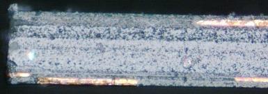

190 Figure 90 Batch 2b (NELL polymer) Sample E5 after 1000 thermal cycles. 163


191 Figure 91 Two-step dicing (NELL polymer) Sample E4 after 1000 thermal cycles. 164


192 Figure 92 Batch 3a (NELL polymer) Sample F1 after 1000 thermal cycles. 165
193 Figure 93 Batch 3b (NELL polymer) Sample F2 after 1000 thermal cycles. 166
 (c)")
 (e)")
 (f)")


194 (a) (b) (h) (c) (g) (d) (f) (e) (a) (e) (b) (f) (c) (g) (d) (h) Figure 94 Sample A-2b (ABF GX-92) at t0. 167
 (f) (e) (a) (e)")
 Figure 95 Sample")

195 (a) (b) (h) (c) (g) (d) (f) (e) (a) (e) (b) (f) (c) (g) (d) (h) Figure 95 Sample A-2b (ABF GX-92) after 1000 thermal cycles. 168
 (c)")
 (e)")
 (f)")


196 (a) (b) (h) (c) (g) (d) (f) (e) (a) (e) (b) (f) (c) (g) (d) (h) Figure 96 Sample C2-R (50%) (ABF GX-92) after 1000 thermal cycles. 169
 (c)")
 (e)")
 (f)")


197 (a) (b) (h) (c) (g) (d) (f) (e) (a) (e) (b) (f) (c) (g) (d) (h) Figure 97 Sample D2-R (75%) (ABF GX-92) after 1000 thermal cycles. 170
 (c)")
 (e)")
 (f)")


198 (a) (b) (h) (c) (g) (d) (f) (e) (a) (e) (b) (f) (c) (g) (d) (h) Figure 98 Sample F2-L (75%) (ABF GX-92) after 50 thermal cycles. 171
 after 250 thermal cycles.")
199 Figure 99 Sample E1-L (50%) (ABF GX-92) after 250 thermal cycles. 172
Study of Cracking of Thin Glass Interposers Intended for Microelectronic Packaging Substrates
 Study of Cracking of Thin Glass Interposers Intended for Microelectronic Packaging Substrates Scott R. McCann 1,2, Yoichiro Sato 3, Venkatesh Sundaram 1,4, Rao R. Tummala 1,4,5, and Suresh K. Sitaraman
Thermo-Mechanical Reliability of Through-Silicon Vias (TSVs)
") 1 Thermo-Mechanical Reliability of Through-Silicon Vias (TSVs) Xi Liu Ph.D. Student and Suresh K. Sitaraman, Ph.D. Professor The George W. Woodruff School of Mechanical Engineering Georgia Institute of
1 Thermo-Mechanical Reliability of Through-Silicon Vias (TSVs) Xi Liu Ph.D. Student and Suresh K. Sitaraman, Ph.D. Professor The George W. Woodruff School of Mechanical Engineering Georgia Institute of
178 IEEE TRANSACTIONS ON COMPONENTS, PACKAGING AND MANUFACTURING TECHNOLOGY, VOL. 7, NO. 2, FEBRUARY 2017
 178 IEEE TRANSACTIONS ON COMPONENTS, PACKAGING AND MANUFACTURING TECHNOLOGY, VOL. 7, NO. 2, FEBRUARY 2017 Experimental and Theoretical Assessment of Thin Glass Substrate for Low Warpage Scott McCann, Vanessa
Atul Gupta, Eric Snyder, Christiane Gottschalk, Kevin Wenzel, James Gunn
 First Demonstration of Photoresist Cleaning for Fine-Line RDL Yield Enhancement by an Innovative Ozone Treatment Process for Panel Fan-out and Interposers Atul Gupta, Eric Snyder, Christiane Gottschalk,
Board-Level Reliability of 3D Through Glass Via Filters During Thermal Cycling
 Board-Level Reliability of 3D Through Glass Via Filters During Thermal Cycling Scott McCann 12*, Satoru Kuramochi 3, Hobie Yun 4, Venkatesh Sundaram 1, M. Raj Pulugurtha 1, Rao R. Tummala 1, and Suresh
TGV and Integrated Electronics
 TGV and Integrated Electronics Shin Takahashi ASAHI GLASS CO., LTD. 1 Ambient Intelligence Green Energy/Environment Smart Factory Smart Mobility Smart Mobile Devices Bio/Medical Security/Biometrics 2 Glass
Packaging Effect on Reliability for Cu/Low k Damascene Structures*
 Packaging Effect on Reliability for Cu/Low k Damascene Structures* Guotao Wang and Paul S. Ho Laboratory of Interconnect & Packaging, TX 78712 * Work supported by SRC through the CAIST Program TRC 2003
/15/$ IEEE Electronic Components & Technology Conference
 Demonstration of 2µm RDL Wiring Using Dry Film Photoresists and 5µm RDL Via by Projection Lithography for Low-cost 2.5D Panel-based Glass and Organic Interposers Ryuta Furuya*, Hao Lu**, Fuhan Liu**, Hai
Innovative Substrate Technologies in the Era of IoTs
 Innovative Substrate Technologies in the Era of IoTs Dyi- Chung Hu 胡迪群 September 4, 2015 Unimicron Contents Introduction Substrate Technology - Evolution Substrate Technology - Revolution Glass substrate
Chips Face-up Panelization Approach For Fan-out Packaging
 Chips Face-up Panelization Approach For Fan-out Packaging Oct. 15, 2015 B. Rogers, D. Sanchez, C. Bishop, C. Sandstrom, C. Scanlan, TOlson T. REV A Background on FOWLP Fan-Out Wafer Level Packaging o Chips
Flip Chip - Integrated In A Standard SMT Process
 Flip Chip - Integrated In A Standard SMT Process By Wilhelm Prinz von Hessen, Universal Instruments Corporation, Binghamton, NY This paper reviews the implementation of a flip chip product in a typical
Novel Materials and Activities for Next Generation Package. Hitachi Chemical., Co.Ltd. Packaging Solution Center Hiroaki Miyajima
 Novel Materials and Activities for Next Generation Package Hitachi Chemical., Co.Ltd. Packaging Solution Center Hiroaki Miyajima 1. Activities of Packaging Solution Center 2. Novel Materials for Next Gen.
Challenges and Solutions for Cost Effective Next Generation Advanced Packaging. H.P. Wirtz, Ph.D. MiNaPAD Conference, Grenoble April 2012
 Challenges and Solutions for Cost Effective Next Generation Advanced Packaging H.P. Wirtz, Ph.D. MiNaPAD Conference, Grenoble April 2012 Outline Next Generation Package Requirements ewlb (Fan-Out Wafer
Panel Discussion: Advanced Packaging
 Dr. Steve Bezuk Senior Director IC Packaging Engineering Qualcomm Technologies, Inc. Panel Discussion: Advanced Packaging PAGE 1 Technical Challenges of Packaging (Mobile Focus) Materials Die materials
II. A. Basic Concept of Package.
 Wafer Level Package for Image Sensor Module Won Kyu Jeung, Chang Hyun Lim, Jingli Yuan, Seung Wook Park Samsung Electro-Mechanics Co., LTD 314, Maetan3-Dong, Yeongtong-Gu, Suwon, Gyunggi-Do, Korea 440-743
IMPLEMENTATION OF A FULLY MOLDED FAN-OUT PACKAGING TECHNOLOGY
 IMPLEMENTATION OF A FULLY MOLDED FAN-OUT PACKAGING TECHNOLOGY B. Rogers, C. Scanlan, and T. Olson Deca Technologies, Inc. Tempe, AZ USA boyd.rogers@decatechnologies.com ABSTRACT Fan-Out Wafer-Level Packaging
"ewlb Technology: Advanced Semiconductor Packaging Solutions"
 "ewlb Technology: Advanced Semiconductor Packaging Solutions" by Sharma Gaurav@, S.W. Yoon, Yap Yok Mian, Shanmugam Karthik, Yaojian Lin, Pandi C. Marimuthu and Yeong J. Lee* STATS ChipPAC Ltd. 5 Yishun
Simulation of Embedded Components in PCB Environment and Verification of Board Reliability
 Simulation of Embedded Components in PCB Environment and Verification of Board Reliability J. Stahr, M. Morianz AT&S Leoben, Austria M. Brizoux, A. Grivon, W. Maia Thales Global Services Meudon-la-Forêt,
Copyright 2009 Year IEEE. Reprinted from 2009 Electronic Components and Technology Conference. Such permission of the IEEE does not in any way imply
 Copyright 2009 Year IEEE. Reprinted from 2009 Electronic Components and Technology Conference. Such permission of the IEEE does not in any way imply IEEE endorsement of any of Institute of Microelectronics
Cost effective 300mm Large Scale ewlb (embedded Wafer Level BGA) Technology
 Technology") Cost effective 300mm Large Scale ewlb (embedded Wafer Level BGA) Technology by Meenakshi Prashant, Seung Wook Yoon, Yaojian LIN and Pandi C. Marimuthu STATS ChipPAC Ltd. 5 Yishun Street 23, Singapore 768442
Cost effective 300mm Large Scale ewlb (embedded Wafer Level BGA) Technology by Meenakshi Prashant, Seung Wook Yoon, Yaojian LIN and Pandi C. Marimuthu STATS ChipPAC Ltd. 5 Yishun Street 23, Singapore 768442
Avatrel Stress Buffer Coatings: Low Stress Passivation and Redistribution Applications
 Avatrel Stress Buffer Coatings: Low Stress Passivation and Redistribution Applications Ed Elce, Chris Apanius, Jeff Krotine, Jim Sperk, Andrew Bell, Rob Shick* Sue Bidstrup-Allen, Paul Kohl Takashi Hirano,
Chip-Packaging Interaction and Reliability Impact on Cu/Low-k Interconnects. Mechanics, University of Texas, Austin, TX 78712
 Chip-Packaging Interaction and Reliability Impact on Cu/Low-k Interconnects Xuefeng Zhang 1, Se Hyuk Im 2, Rui Huang 2, and Paul S. Ho 1 1 Microelectronics Research Center, 2 Department of Aerospace Engineering
Plasma for Underfill Process in Flip Chip Packaging
 Plasma for Underfill Process in Flip Chip Packaging Jack Zhao and James D. Getty Nordson MARCH 2470-A Bates Avenue Concord, California 94520-1294 USA Published by Nordson MARCH www.nordsonmarch.com 2015
IME Proprietary. EPRC 12 Project Proposal. 3D Embedded WLP. 15 th August 2012
 EPRC 12 Project Proposal 3D Embedded WLP 15 th August 2012 Motivation Factors driving IC market Higher density, lower cost, high yield Fan-out WLP/eWLP advantages Small footprint, low profile Low cost,
Welcome to Streamline Circuits Lunch & Learn. Design for Reliability & Cost Reduction of Advanced Rigid-Flex/Flex PCB Technology
 Welcome to Streamline Circuits Lunch & Learn Design for Reliability & Cost Reduction of Advanced Rigid-Flex/Flex PCB Technology Accurate PCB data is critical to the tooling process. Here are some key items
JOINT INDUSTRY STANDARD
 JOINT INDUSTRY STANDARD AUGUST 1999 Semiconductor Design Standard for Flip Chip Applications ASSOCIATION CONNECTING ELECTRONICS INDUSTRIES Semiconductor Design Standard for Flip Chip Applications About
3D Packaging- Synthetic Quartz Substrate and Interposers for High Frequency Applications. Vern Stygar #1, Tim Mobley* 2 # Asahi Glass Corporation
 3D Packaging- Synthetic Quartz Substrate and Interposers for High Frequency Applications Vern Stygar #1, Tim Mobley* 2 # Asahi Glass Corporation 4375 Northwest 235 th Avenue, Hillsboro OR USA 97124 1 vstygar@agem.com
3DIC Integration with TSV Current Progress and Future Outlook
 3DIC Integration with TSV Current Progress and Future Outlook Shan Gao, Dim-Lee Kwong Institute of Microelectronics, A*STAR (Agency for Science, Technology and Research) Singapore 9 September, 2010 1 Overview
Embedded Trench Redistribution Layers (RDL) by Excimer Laser Ablation and Surface Planer Processes
 by Excimer Laser Ablation and Surface Planer Processes") Embedded Trench Redistribution Layers (RDL) by Excimer Laser Ablation and Surface Planer Processes Yuya Suzuki, Venky Sundaram, Rao Tummala Georgia Insitute of Technology 3D Systems Packaging Research
Embedded Trench Redistribution Layers (RDL) by Excimer Laser Ablation and Surface Planer Processes Yuya Suzuki, Venky Sundaram, Rao Tummala Georgia Insitute of Technology 3D Systems Packaging Research
Micro-Electro-Mechanical Systems (MEMS) Fabrication. Special Process Modules for MEMS. Principle of Sensing and Actuation
 Fabrication. Special Process Modules for MEMS. Principle of Sensing and Actuation") Micro-Electro-Mechanical Systems (MEMS) Fabrication Fabrication Considerations Stress-Strain, Thin-film Stress, Stiction Special Process Modules for MEMS Bonding, Cavity Sealing, Deep RIE, Spatial forming
Micro-Electro-Mechanical Systems (MEMS) Fabrication Fabrication Considerations Stress-Strain, Thin-film Stress, Stiction Special Process Modules for MEMS Bonding, Cavity Sealing, Deep RIE, Spatial forming
MEPTEC Semiconductor Packaging Technology Symposium
 MEPTEC Semiconductor Packaging Technology Symposium Advanced Packaging s Interconnect Technology Process Shift and Direction October 23, 2014 Jay Hayes- Director of Business Development -Bumping and Flip
1 Thin-film applications to microelectronic technology
 1 Thin-film applications to microelectronic technology 1.1 Introduction Layered thin-film structures are used in microelectronic, opto-electronic, flat panel display, and electronic packaging technologies.
2.5D and 3D Semiconductor Package Technology: Evolution and Innovation
 2.5D and 3D Semiconductor Package Technology: Evolution and Innovation Vern Solberg Solberg Technical Consulting Saratoga, California USA Abstract The electronics industry is experiencing a renaissance
Cu Pillar Interconnect and Chip-Package-Interaction (CPI) for Advanced Cu Low K chip
 for Advanced Cu Low K chip") EPRC 12 Project Proposal Cu Pillar Interconnect and Chip-Package-Interaction (CPI) for Advanced Cu Low K chip 15 th Aug 2012 Page 1 Introduction: Motivation / Challenge Silicon device with ultra low k
EPRC 12 Project Proposal Cu Pillar Interconnect and Chip-Package-Interaction (CPI) for Advanced Cu Low K chip 15 th Aug 2012 Page 1 Introduction: Motivation / Challenge Silicon device with ultra low k
Thermo-Mechanical Reliability Assessment of TSV Die Stacks by Finite Element Analysis
 Thermo-Mechanical Reliability Assessment of TSV Die Stacks by Finite Element Analysis Dr. Roland Irsigler, emens AG Corporate Technology, CT T P HTC Outline TSV SOLID µbump Stacking TSV application FEA
Design and Assembly Process Implementation of 3D Components
 IPC-7091 Design and Assembly Process Implementation of 3D Components Developed by the 3-D Electronic Packages Subcommittee (B-11) of the Packaged Electronic Components Committee (B-10) of IPC Users of
Challenges and Future Directions of Laser Fuse Processing in Memory Repair
 Challenges and Future Directions of Laser Fuse Processing in Memory Repair Bo Gu, * T. Coughlin, B. Maxwell, J. Griffiths, J. Lee, J. Cordingley, S. Johnson, E. Karagiannis, J. Ehrmann GSI Lumonics, Inc.
3D technologies for integration of MEMS
 3D technologies for integration of MEMS, Fraunhofer Institute for Electronic Nano Systems Folie 1 Outlook Introduction 3D Processes Process integration Characterization Sample Applications Conclusion Folie
Molding materials performances experimental study for the 3D interposer scheme
 Minapad 2014, May 21 22th, Grenoble; France Molding materials performances experimental study for the 3D interposer scheme Y. Sinquin, A. Garnier, M. Argoud, A. Jouve, L. Baud, J. Dechamp, N. Allouti,
Thermo-Mechanical FEM Analysis of Lead Free and Lead Containing Solder for Flip Chip Applications
 Thermo-Mechanical FEM Analysis of Lead Free and Lead Containing Solder for Flip Chip Applications M. Gonzalez 1, B. Vandevelde 1, Jan Vanfleteren 2 and D. Manessis 3 1 IMEC, Kapeldreef 75, 3001, Leuven,
23 rd ASEMEP National Technical Symposium
 THE EFFECT OF GLUE BOND LINE THICKNESS (BLT) AND FILLET HEIGHT ON INTERFACE DELAMINATION Raymund Y. Agustin Janet M. Jucar Jefferson S. Talledo Corporate Packaging & Automation/ Q&R STMicroelectronics,
3D FRACTURE MECHANICS ANALYSIS OF UNDERFILL DELAMINATION FOR FLIP CHIP PACKAGES
 3D FRACTURE MECHANICS ANALYSIS OF UNDERFILL DELAMINATION FOR FLIP CHIP PACKAGES Zhen Zhang, Charlie J Zhai, and Raj N Master Advanced Micro Devices, Inc. 1050 E. Arques Ave., Sunnyvale, CA 94085, USA Phone:
Board Level Reliability Improvement in ewlb (Embedded Wafer Level BGA) Packages
 Packages") Board Level Reliability Improvement in ewlb (Embedded Wafer Level BGA) Packages by Seng Guan Chow, Yaojian Lin, Bernard Adams * and Seung Wook Yoon** STATS ChipPAC Ltd. 5 Yishun Street 23, Singapore 768442
Board Level Reliability Improvement in ewlb (Embedded Wafer Level BGA) Packages by Seng Guan Chow, Yaojian Lin, Bernard Adams * and Seung Wook Yoon** STATS ChipPAC Ltd. 5 Yishun Street 23, Singapore 768442
Improvement of Laser Fuse Processing of Fine Pitch Link Structures for Advanced Memory Designs
 Improvement of Laser Fuse Processing of Fine Pitch Link Structures for Advanced Memory Designs Joohan Lee, Joseph J. Griffiths, and James Cordingley GSI Group Inc. 60 Fordham Rd. Wilmington, MA 01887 jlee@gsig.com
FABRICATION AND RELIABILITY OF ULTRA-FINE RDL STRUCTURES IN ADVANCED PACKAGING BY EXCIMER LASER ABLATION
 FABRICATION AND RELIABILITY OF ULTRA-FINE RDL STRUCTURES IN ADVANCED PACKAGING BY EXCIMER LASER ABLATION NCCAVS Joint Users Group Technical Symposium San Jose, June 7 th, 2017 Markus Arendt, SÜSS MicroTec
Warpage Mechanism of Thin Embedded LSI Packages
 Nakashima et al.: Warpage Mechanism of Thin Embedded LSI Packages (1/10) [Technical Paper] Warpage Mechanism of Thin Embedded LSI Packages Yoshiki Nakashima*, Katsumi Kikuchi*, Kentaro Mori*, Daisuke Ohshima**,
System Level Effects on Solder Joint Reliability
 System Level Effects on Solder Joint Reliability Maxim Serebreni 2004 2010 Outline Thermo-mechanical Fatigue of solder interconnects Shear and tensile effects on Solder Fatigue Effect of Glass Style on
Fraunhofer ENAS Current results and future approaches in Wafer-level-packaging FRANK ROSCHER
 Fraunhofer ENAS - Current results and future approaches in Wafer-level-packaging FRANK ROSCHER Fraunhofer ENAS Chemnitz System Packaging Page 1 System Packaging Outline: Wafer level packaging for MEMS
Effects of Design, Structure and Material on Thermal-Mechanical Reliability of Large Array Wafer Level Packages
 Effects of Design, Structure and Material on Thermal-Mechanical Reliability of Large Array Wafer Level Packages Bhavesh Varia 1, Xuejun Fan 1, 2, Qiang Han 2 1 Department of Mechanical Engineering Lamar
MODELING, DESIGN, FABRICATION AND CHARACTERIZATTION OF GLASS PACKAGE-TO-PCB INTERCONNECTIONS
 MODELING, DESIGN, FABRICATION AND CHARACTERIZATTION OF GLASS PACKAGE-TO-PCB INTERCONNECTIONS A Thesis Presented to The Academic Faculty by GARY QUENTIN MENEZES In Partial Fulfillment of the Requirements
Advanced Materials for Thermal Management of Electronic Packaging
 Xingcun Colin Tong Advanced Materials for Thermal Management of Electronic Packaging Sprin ger Contents 1 Thermal Management Fundamentals and Design Guides in Electronic Packaging 1 Rationale of Thermal
SUSS SOLUTIONS FOR LARGE FORMAT PATTERNING UV Scanning Lithography and Excimer Laser Ablation
 SUSS SOLUTIONS FOR LARGE FORMAT PATTERNING UV Scanning Lithography and Excimer Laser Ablation Kevin Yang, Habib Hichri, Ralph Zoberbier SÜSS MicroTec Photonic Systems Inc. June 18, 2015 MARKET DRIVER Mobile
By Ron Blankenhorn, Pac Tech USA, Santa Clara, Calif., and Thomas Oppert, Pac Tech GbmH, Nauen, Germany
 INTRODUCTION Modern microelectronic products require packages that address the driving forces of reduced size and weight, as well as increased performance at high frequencies. Flipchip and direct chip
Silver Diffusion Bonding and Layer Transfer of Lithium Niobate to Silicon
 Chapter 5 Silver Diffusion Bonding and Layer Transfer of Lithium Niobate to Silicon 5.1 Introduction In this chapter, we discuss a method of metallic bonding between two deposited silver layers. A diffusion
726 IEEE TRANSACTIONS ON COMPONENTS, PACKAGING AND MANUFACTURING TECHNOLOGY, VOL. 7, NO. 5, MAY 2017
 726 IEEE TRANSACTIONS ON COMPONENTS, PACKAGING AND MANUFACTURING TECHNOLOGY, VOL. 7, NO. 5, MAY 2017 Board-Level Thermal Cycling and Drop-Test Reliability of Large, Ultrathin Glass BGA Packages for Smart
3D Package Technologies Review with Gap Analysis for Mobile Application Requirements. Apr 22, 2014 STATS ChipPAC Japan
 3D Package Technologies Review with Gap Analysis for Mobile Application Requirements Apr 22, 2014 STATS ChipPAC Japan T.Nishio Contents Package trends and roadmap update Advanced technology update Fine
Verifying The Reliability Of Connections In HDI PWBs
 Verifying The Reliability Of Connections In HDI PWBs The stacking of via holes is used effectively in the development of high density circuits on build-up printed wiring boards (PWBs). However, when micro
Failure Modes in Wire bonded and Flip Chip Packages
 Failure Modes in Wire bonded and Flip Chip Packages Mumtaz Y. Bora Peregrine Semiconductor San Diego, Ca. 92121 mbora@psemi.com Abstract The growth of portable and wireless products is driving the miniaturization
Lecture 22: Integrated circuit fabrication
 Lecture 22: Integrated circuit fabrication Contents 1 Introduction 1 2 Layering 4 3 Patterning 7 4 Doping 8 4.1 Thermal diffusion......................... 10 4.2 Ion implantation.........................
Thin Wafers Bonding & Processing
 Thin Wafers Bonding & Processing A market perspective 2012 Why New Handling Technologies Consumer electronics is today a big driver for smaller, higher performing & lower cost device configurations. These
MODELING, DESIGN, FABRICATION AND RELIABILITY CHARACTERIZATION OF ULTRA-THIN, GLASS BGA PACKAGE-TO- BOARD INTERCONNECTIONS
 MODELING, DESIGN, FABRICATION AND RELIABILITY CHARACTERIZATION OF ULTRA-THIN, GLASS BGA PACKAGE-TO- BOARD INTERCONNECTIONS A Thesis Presented to The Academic Faculty By Bhupender Singh In Partial Fulfillment
Power Electronics Packaging Solutions for Device Junction Temperature over 220 o C
 EPRC 12 Project Proposal Power Electronics Packaging Solutions for Device Junction Temperature over 220 o C 15 th August 2012 Page 1 Motivation Increased requirements of high power semiconductor device
14. Designing with FineLine BGA Packages
 14. Designing with FineLine BGA Packages S51014-1.0 Chapter 14, Designing with FineLine BGA Packages, replaces AN 114: Designing with FineLine BGA Packages. Introduction As programmable logic devices (PLDs)
Basic PCB Level Assembly Process Methodology for 3D Package-on-Package
 Basic PCB Level Assembly Process Methodology for 3D Package-on-Package Vern Solberg STC-Madison Madison, Wisconsin USA Abstract The motivation for developing higher density IC packaging continues to be
Experience in Applying Finite Element Analysis for Advanced Probe Card Design and Study. Krzysztof Dabrowiecki Jörg Behr
 Experience in Applying Finite Element Analysis for Advanced Probe Card Design and Study Krzysztof Dabrowiecki Jörg Behr Overview A little bit of history in applying finite element analysis for probe card
OPTIMAL SELECTION OF PROCESS PARAMETERS OF ULTRASONIC MACHINING (USM) SYSTEM
 SYSTEM") OPTIMAL SELECTION OF PROCESS PARAMETERS OF ULTRASONIC MACHINING (USM) SYSTEM BY H. L A L C H H U A N V E L A B.E. (Mech), MNNIT, Allahabad (Formerly M.N.R.E.C., Allahabad), 1987; M.Tech. (Mech), IT-BHU,
OPTIMAL SELECTION OF PROCESS PARAMETERS OF ULTRASONIC MACHINING (USM) SYSTEM BY H. L A L C H H U A N V E L A B.E. (Mech), MNNIT, Allahabad (Formerly M.N.R.E.C., Allahabad), 1987; M.Tech. (Mech), IT-BHU,
Recent Advances in Die Attach Film
 Recent Advances in Die Attach Film Frederick Lo, Maurice Leblon, Richard Amigh, and Kevin Chung. AI Technology, Inc. 70 Washington Road, Princeton Junction, NJ 08550 www.aitechnology.com Abstract: The
Enabling Technology in Thin Wafer Dicing
 Enabling Technology in Thin Wafer Dicing Jeroen van Borkulo, Rogier Evertsen, Rene Hendriks, ALSI, platinawerf 2G, 6641TL Beuningen Netherlands Abstract Driven by IC packaging and performance requirements,
CHARACTERISATION OF INTERFACIAL CRACKING IN MICROELECTRONIC PACKAGING
 CHARACTERISATION OF INTERFACIAL CRACKING IN MICROELECTRONIC PACKAGING Ian McEnteggart Microelectronics Business Manager Instron Limited, Coronation Road, High Wycombe, Buckinghamshire HP12 3SY www.instron.com/microelectronics
Images of Failures in Microelectronics Packaging and Assembly
 Images of Failures in Microelectronics Packaging and Assembly Ed Hare, Ph.D./SEM Lab, Inc. IMAPS NW - Feb. 11th 2004 Redmond, WA http://www.semlab.com 1 What is this? http://www.semlab.com 2 Inner Layer
Evaluation of length scale effects for micro and nano-sized cantilevered structures
 University of Wollongong Research Online University of Wollongong Thesis Collection 1954-2016 University of Wollongong Thesis Collections 2010 Evaluation of length scale effects for micro and nano-sized
Optimizing the Insulated Metal Substrate Application with Proper Material Selection and Circuit Fabrication
 Abstract Optimizing the Insulated Metal Substrate Application with Proper Material Selection and Circuit Fabrication Dave Sommervold, Chris Parker, Steve Taylor, Garry Wexler. The Bergquist Company Prescott,
Final Year Project Proposal 1
 Final Year Project Proposal 1 Mechanical testing for high temperature polymers Mr Eric Phua Jian Rong (JRPhua@ntu.edu.sg) In offshore subsea drilling, different types of microelectronics devices and sensors
Integrated Copper Heat Slugs and EMI Shields in Panel Laminate (LFO) and Glass Fanout (GFO) Packages for High Power RF ICs
 and Glass Fanout (GFO) Packages for High Power RF ICs") Integrated Copper Heat Slugs and EMI Shields in Panel Laminate (LFO) and Glass Fanout (GFO) Packages for High Power RF ICs Venky Sundaram, Bartlet Deprospo, Nahid Gezgin, Atomu Watanabe, P. Markondeya
Integrated Copper Heat Slugs and EMI Shields in Panel Laminate (LFO) and Glass Fanout (GFO) Packages for High Power RF ICs Venky Sundaram, Bartlet Deprospo, Nahid Gezgin, Atomu Watanabe, P. Markondeya
Flexible Printed Circuits Design Guide
 www.tech-etch.com/flex Flexible Printed Circuits Design Guide Multilayer SMT Assembly Selective Plating of Gold & Tin-Lead Fine Line Microvias Cantilevered & Windowed Leads 1 MATERIALS CONDUCTOR Copper
NANO SCRATCH TESTING OF THIN FILM ON GLASS SUBSTRATE
 NANO SCRATCH TESTING OF THIN FILM ON GLASS SUBSTRATE Prepared by Jesse Angle 6 Morgan, Ste156, Irvine CA 92618 P: 949.461.9292 F: 949.461.9232 nanovea.com Today's standard for tomorrow's materials. 2010
c/bach, 2-B Pol. Ind Foinvasa Montcada i Reixac (Barcelona) SPAIN Tel FAX
 SPAIN Tel FAX") 1- What is 2- How does it work? 3- How do we make it? 4- Applications 5- Processing? WHAT IS? Thick aluminium based substrate, cladded in ED copper foil. Designed for an effective thermal dissipation and
1- What is 2- How does it work? 3- How do we make it? 4- Applications 5- Processing? WHAT IS? Thick aluminium based substrate, cladded in ED copper foil. Designed for an effective thermal dissipation and
Chapter 3 Silicon Device Fabrication Technology
 Chapter 3 Silicon Device Fabrication Technology Over 10 15 transistors (or 100,000 for every person in the world) are manufactured every year. VLSI (Very Large Scale Integration) ULSI (Ultra Large Scale
Analog Devices ADSP KS-160 SHARC Digital Signal Processor
 Construction Analysis Analog Devices ADSP-21062-KS-160 SHARC Digital Signal Processor Report Number: SCA 9712-575 Global Semiconductor Industry the Serving Since 1964 17350 N. Hartford Drive Scottsdale,
Preface... VII ForewordbyDr.FranzAlt... IX Foreword by Dr. Hermann Scheer... XIII Table of Contents... XV. 1.3 Global warming by CO
 Contents Preface... VII ForewordbyDr.FranzAlt... IX Foreword by Dr. Hermann Scheer... XIII Table of Contents.... XV 1 Introduction...1 1.1 World s Energy Consumption...1 1. CO -Emissions by Humankind...
Three-Dimensional Molded Interconnect Devices (3D-MID)
") Jörg Frank Three-Dimensional Molded Interconnect Devices (3D-MID) Materials, Manufacturing, Assembly and Applica ons for Injec on Molded Circuit Carriers Sample Pages ISBN 978-1-56990-551-7 HANSER Hanser
Jörg Frank Three-Dimensional Molded Interconnect Devices (3D-MID) Materials, Manufacturing, Assembly and Applica ons for Injec on Molded Circuit Carriers Sample Pages ISBN 978-1-56990-551-7 HANSER Hanser
Recent Trends of Package Warpage and Measurement Metrologies (inemi Warpage Characterization Project Phase 3)
") Recent Trends of Package Warpage and Measurement Metrologies (inemi Warpage Characterization Project Phase 3) Wei Keat Loh 1, Ron Kulterman 2, Haley Fu 3, Masahiro Tsuriya 3 1 Intel Technology Sdn. Bhd.
Recent Trends of Package Warpage and Measurement Metrologies (inemi Warpage Characterization Project Phase 3) Wei Keat Loh 1, Ron Kulterman 2, Haley Fu 3, Masahiro Tsuriya 3 1 Intel Technology Sdn. Bhd.
TSV Processing and Wafer Stacking. Kathy Cook and Maggie Zoberbier, 3D Business Development
 TSV Processing and Wafer Stacking Kathy Cook and Maggie Zoberbier, 3D Business Development Outline Why 3D Integration? TSV Process Variations Lithography Process Results Stacking Technology Wafer Bonding
Nanium Overview. Company Presentation
 Nanium Overview Company Presentation Nanium Overview Our name and logo nano prefix of Greek origin referring to small objects ium suffix of Latin origin that includes the formation of scientific terms
Reliability Challenges for 3D Interconnects:
 Reliability Challenges for 3D Interconnects: A material and design perspective Paul S. Ho Suk-Kyu Ryu, Kuan H. (Gary) Lu, Qiu Zhao, Jay Im and Rui Huang The University of Texas at Austin 3D Sematech Workshop,
Materials Characterization for Stress Management
 Materials Characterization for Stress Management Ehrenfried Zschech, Fraunhofer IZFP Dresden, Germany Workshop on Stress Management for 3D ICs using TSVs San Francisco/CA, July 13, 2010 Outline Stress
System-in-Package (SiP) on Wafer Level, Enabled by Fan-Out WLP (ewlb)
 on Wafer Level, Enabled by Fan-Out WLP (ewlb)") System-in-Package (SiP) on Wafer Level, Enabled by Fan-Out WLP (ewlb) Steffen Kröhnert, José Campos, Eoin O Toole NANIUM S.A., Vila do Conde, Portugal Outline Short Company Overview NANIUM Introduction
System-in-Package (SiP) on Wafer Level, Enabled by Fan-Out WLP (ewlb) Steffen Kröhnert, José Campos, Eoin O Toole NANIUM S.A., Vila do Conde, Portugal Outline Short Company Overview NANIUM Introduction
Reliability Evaluation of CIF (chip-in-flex) and COF (chip-on-flex) packages
 and COF (chip-on-flex) packages") Reliability Evaluation of CIF (chip-in-flex) and COF (chip-on-flex) packages Jae-Won Jang* a, Kyoung-Lim Suk b, Kyung-Wook Paik b, and Soon-Bok Lee a a Dept. of Mechanical Engineering, KAIST, 335 Gwahangno
Reliability Evaluation of CIF (chip-in-flex) and COF (chip-on-flex) packages Jae-Won Jang* a, Kyoung-Lim Suk b, Kyung-Wook Paik b, and Soon-Bok Lee a a Dept. of Mechanical Engineering, KAIST, 335 Gwahangno
Solder joint reliability of cavity-down plastic ball grid array assemblies
 cavity-down plastic ball grid array S.-W. Ricky Lee Department of Mechanical Engineering, The Hong Kong University of Science and, Kowloon, Hong Kong John H. Lau Express Packaging Systems, Inc., Palo Alto,
FABRICATION ENGINEERING MICRO- NANOSCALE ATTHE AND. Fourth Edition STEPHEN A. CAMPBELL. of Minnesota. University OXFORD UNIVERSITY PRESS
 AND FABRICATION ENGINEERING ATTHE MICRO- NANOSCALE Fourth Edition STEPHEN A. CAMPBELL University of Minnesota New York Oxford OXFORD UNIVERSITY PRESS CONTENTS Preface xiii prrt i OVERVIEW AND MATERIALS
IPC-AJ-820A Assembly and Joining Handbook. The How and Why of All Things PCB & PCA
 IPC-AJ-820A Assembly and Joining Handbook The How and Why of All Things PCB & PCA 1 Scope To provide guidelines and supporting info for the mfg of electronic equipment To explain the HOW TO and WHY Discussions
OPTIMIZED SEMI-ADDITIVE PROCESS FOR POLYIMIDE AS DIELECTRIC IN BUILD UP PACKAGES
 OPTIMIZED SEMI-ADDITIVE PROCESS FOR POLYIMIDE AS DIELECTRIC IN BUILD UP PACKAGES Fei Peng 1, Ernest Long 1, Jim Watkowski 1, Kesheng Feng 1, Naomi Ando 2, Kazuhiro Inazu 2 1 MacDermid, 227 Freight St,
Advances in Printing nano Cu and Using Existing Cu Based Manufacturing Processes. Michael J. Carmody Chief Scientist, Intrinsiq Materials
 Advances in Printing nano Cu and Using Existing Cu Based Manufacturing Processes Michael J. Carmody Chief Scientist, Intrinsiq Materials Why Use Copper? Lower Cost than Silver. Print on Numerous Substrates.
Ultra Fine Pitch Bumping Using e-ni/au and Sn Lift-Off Processes
 Ultra Fine Pitch Bumping Using e-ni/au and Sn Lift-Off Processes Andrew Strandjord, Thorsten Teutsch, and Jing Li Pac Tech USA Packaging Technologies, Inc. Santa Clara, CA USA 95050 Thomas Oppert, and
EDGE CHIPPING RESISTANCE USING MACROINDENTATION TESTING
 EDGE CHIPPING RESISTANCE USING MACROINDENTATION TESTING Prepared by Ali Mansouri 6 Morgan, Ste156, Irvine CA 92618 P: 949.461.9292 F: 949.461.9232 nanovea.com Today's standard for tomorrow's materials.
Effect of Chip Dimension and Substrate Thickness on the Solder Joint Reliability of Plastic Ball Grid Array Packages* S.-W. Lee, J.H.
 Page 1 of 9 Effect of Chip Dimension and Substrate Thickness on the Solder Joint Reliability of Plastic Ball Grid Array Packages* The Authors S.-W. Lee, J.H. Lau** S.-W. Lee, Center for Advanced Engineering
System in Package: Identified Technology Needs from the 2004 inemi Roadmap
 System in Package: Identified Technology Needs from the 2004 inemi Roadmap James Mark Bird Amkor Technology Inc System in package (SiP) technology has grown significantly in the past several years. It
Leveraging the Precision of Electroforming over Alternative Processes When Developing Nano-scale Structures
 VOLUME 4 - ELECTROFORMING Leveraging the Precision of over Alternative Processes When Developing Nano-scale Structures Electrical and mechanical component and subsystem designers generally have five techniques