CMP Defects and Evolution of PCMP Cleans
|
|
|
- Easter Bell
- 6 years ago
- Views:
Transcription

1 CMP Defects and Evolution of PCMP Cleans March 27, 2017 Iqbal Ali (408) SPCC & PCMP Conference, Austin, TX
2 Agenda 1. Introduction to Linx Consulting 2. Where Have We Been and Where are We Going? 3. Defects in CMP 4. Post-CMP Clean 5. Conclusions 2
3 Introduction to Linx Consulting 3
4 Linx Consulting 1. We help our clients to succeed by creating knowledge and developing unique insights at the intersection of electronic thin film processes and the chemicals industry 2. The knowledge is based on a core understanding of the semiconductor device technology; manufacturing processes and roadmaps; and the structural industry dynamics 3. This knowledge is leveraged to create advanced models, simulations and real-world forecasts 4. Our perspectives are by direct research and leveraging our extensive experience throughout the global industry value chain, including: Experience in global electronics and advanced materials and thin film processing industries Experience in the global chemicals industry Experience at Device Producers Experience at OEMs 4
5 Linx Consulting Service Portfolio Multi-Client Reports IC Materials CMP Deposition Patterning Cleaning Gases Bulk Chemicals III-Vs, TSV, WLP, Solar Proprietary Projects Market Planning M & A Growth and Diversification Supply Chain Optimization Technology Commercialization Strategic Planning Voice of the Customer Econometric Semiconductor Forecast Financial planning Sales and Operational planning Forecasting Hilltop Economics LLC Cost Modeling Client demand modeling Product development Bill of Materials quantification IC Knowledge, LLC Semi Packaging Nano Technology LCD PV LED/ Compound Semi Conference Production - Surface Prep & Cleaning Conference & PCMP Cleans 5
6 Customer Base in Semiconductors Finance &Technology Raws & Chemicals Equipment Services End-users & Consortia China Taiwan SEA & India North America Korea Europe Japan 6
7 Where Have We Been and Where are We Going? 7

8 Total Cleans Chemicals Market $2,500 millions $2,000 $1,500 $1,000 $500 $ PCMP $122 $132 $147 $163 $175 $186 $192 Solvent Strip $132 $132 $126 $146 $171 $197 $225 Bulk Wets $1,324 $1,316 $1,383 $1,371 $1,401 $1,372 $1,342 PERR $416 $399 $396 $402 $408 $423 $436 8
9 Post CMP Clean Market $250 millions $200 $150 $100 $50 $ W PCMP $24 $27 $30 $32 $34 $35 $34 Oxide PCMP $18 $20 $21 $22 $23 $23 $23 STI PCMP $8 $9 $10 $11 $12 $12 $12 Cu PCMP $71 $76 $86 $97 $106 $116 $123 9
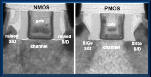
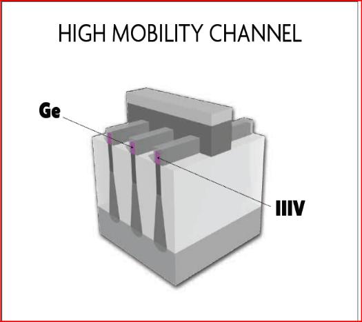
10 Many New Materials Enable Moore s Law Source: ASM (IL: InterfaceLayer) ssoi/geoi Ge IL III-V IL GaN InSb InGaAs Ge STO Ru (PM: Patterning Materials) Other PM's EUV Other PM's EUV Patterning Related BEOL FEOL Starting Materials (*): Projection Co Si(C)P Co Si(C)P FDSOI SiC FDSOI SiC Air SiCO Air SiCO LaO LaO LT SiO LT SiO SiCN SiCN SiCN TiAlC MG ZrO Hf(Si)O AlO TiAlC MG ZrO Hf(Si)O AlO TiAlC MG ZrO Hf(Si)O AlO psioc psioc psioc SOI SOI SOI SiGe(B) SiGe(B) SiGe(B) TaO SOG TaO SOG TaO SOG TaO SOG SiOC Ta/TaN Cu SiOF SiOC Ta/TaN Cu SiOF SiOC Ta/TaN Cu SiOF SiOC Ta/TaN Cu SiOF TiSi PtSi TiSi PtSi TiSi PtSi TiSi PtSi TiSi PtSi TiW TiW TiW/TiN TiN TiN TiN WSi, MoSi WSi, W WSi, W W W W Al BPSG Al BPSG Al BPSG Al BPSG Al BPSG Al BPSG Al BPSG Al SiO, SiN SiO, SiN SiO, SiN SiO, SiN SiO, SiN SiO, SiN SiO, SiN SiO, SiN Si Si Si Si Si Si Si Si (*) 10
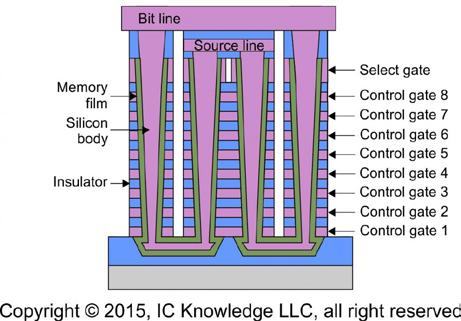
11 New Structures Require CMP Logic NAND EDN Network 11
12 Defects in CMP 12
13 Defectivity Paradigm Shift at 20nm and Beyond 1. Pursuit of Moore s Law is driving ever increasing design innovation, process sensitivity & complexity 2. Paradigm shift in thoughts about what we did not care about earlier in >20nm era & what we care to control now! Complex Chemistry: Compatibility Issues New Defect Sources, increase Defect Sensitivity 3. Metrology techniques of all types are challenged to provide sufficient sensitivity for early detection & prevention Supplier Infrastructure Development needed for better defect detection & characterization Metrology and Quality Control 4. Proactive engagement and collaboration across the supply chain are essential to HVM readiness Source: A. Sengupta, Intel. Semicon West
14 Defects from CMP Process Major defects induced by CMP are caused by: 1. Organic Residue 2. Surface Particle 3. Scratching 4. Surface Flaking 5. Grain Roughness 6. Pattern Damage Due to limited redundancy, each defect directly has an impact on the device performance or yield leads to all kinds are potential killer defect Organic residues and surface particles are the most frequently observed Consumables designed to minimize defects are required including: Ultra-fine/colloidal abrasive Soft pads without sacrificing planarity Mild conditioning with proper pad surface roughness In-situ clean from CMP tool is the most effective for clean wafer since it cleans wafer with wet state 14
15 Metrology Issues Real-time metrology is practically impossible. In-line metrology is challenged to measure critical particle sizes below 20nm High cost of systems Off-line analysis to augment particle characterization Optical (particle detection) systems such as SP3 and SP5 are identifying new defects On-wafer metrology has become the only approach able to show defects. In many cases it is possible to identify the source from on-wafer analysis. The expectation for particle shedding, and contamination continues to reduce. In general, many new defects are driven by the introduction of new materials and processes Killer defects, or critical particles are now in the order of 10 or 20 nm. On-wafer analysis is struggling to define particles sizes or discriminate defects as residues or discrete solids. Defect sources vary from chemicals, water, seals, filters, piping etc. Equipment suppliers are driving to deliver ultraclean products which are certified with the latest analytical techniques, and targeted at delivering best possible performance. 15

16 Defectivity Requirements Impact Consumables For advanced nodes, the industry needs to have extremely tight control on the slurries and pad quality Greater use of high purity particles and chemicals to minimize contamination and increase reproducibility In advanced slurries, quality and morphology of the slurry particles will be critical No agglomerations and angular particles Need mostly spherical particles and to minimize the number of edges Trend to low abrasives or abrasive free 0.5% or lower solids content as the slurry formulation trend is to greater chemo effect than mechanical effect Selectivity requirements will prove challenging to slurries as selectivity is increased tuned as a key point of the overall process control Galvanic corrosion needs to be controlled in-situ this is controlled by using the correct ingredients/formulations Advanced slurry formulations may utilize 10 to 15 distinct ingredients Buff slurries include products from Cabot Micro and Dow/Klebosol In general high purity colloidal silicas are preferred for buffing and there appears to be a trend towards ultra high purity colloidal silica buffs 16

17 Ultra High Purity Colloidal Silica (UHPCS) Fuso manufactures high purity colloidal silica by particle growth method using hydrolysis and condensation with high purity alkoxysilane as a starting material Compared with colloidal silica starting from sodium silicate, this product is more pure, spherical shaped and stable at neutrality The purity of the product excluding nonionic and ionic dispersing agent is % or more It is believed that, based on customer's requirement, it's possible to control particle size, degrees of the particle shape and select the dispersing agent, water, alcohol, glycol, etc. 17

18 Abrasives Selected to Enhance Yield $160 $140 $120 $100 $80 $60 $40 $20 $ Million 11.7% 5.7% -4.9% -14.9% 17.8% 20.0% 15.0% 10.0% 5.0% 0.0% -5.0% -10.0% -15.0% $- Alumina Fumed Silica UHPCS Colloidal Silica Ceria CAGR -20.0% Abrasives that do not drive optimized cost and yield solutions are transitioned away and replaced 18
19 Buffing Can Reduce CMP Defects The industry trend is to use softer pads for barrier polishing to combat scratches on the wafer surface during buffing Typically, higher purity slurry/or wafer clean solutions are used in buffing to reduce microscratches, metallic and ionic contaminants Until recently, the Polytex Supreme was the pad of choice for barrier polishing. However, these pads cause scratches and higher defectivity due to the nature of the pad surface These pads were replaced by Fujibo pads for lower scratches and defectivity The trend now is to use VP3500/3100 pads for better defectivity, lower scratches and better planarity The use of high purity slurry and wafer clean solution have some impact on the output and COO. However, it is well understood that removal of yield limiter defectivity outweighs the slight increase in cost due to buffing Once the polishing process is complete, a post-cmp cleaning process must not only remove residual slurry particles but also trace levels of metal ions, which otherwise could significantly decrease yield 19

20 Replacement Metal Gate (RMG) Process Flow in FinFET Structure Reduction in defectivity Morphology and purity of slurry abrasives Reduction in slurry abrasive content in slurry formulation Advanced polishing pads to reduce microscratches and other defects Reduction in down force for polishing to have minimum abrasion Polisher with advanced features for process control Reduction in post-cmp cleaning contacts Use of ultra-high purity chemicals for slurry formulation Typical Source of Surface Particle Defects Thorough understanding of replacement metal gate (RMG) process flow Look into the integrational aspect of defect source Understanding mechanism of formation of surface particles Role of CMP cleaner module in reducing defects Source: Hong Jin Kim, GF,CAMP

21 Particle Defects at Post Metal Gate CMP Source: Hong Jin Kim, GF, CAMP
22 Post CMP Cleans 22
23 Evolution of PCMP Cleans Due to stringent requirements of defectivity reduction/elimination, steps to remove defectivity from all possible sources are done with extreme care Post-CMP cleaning solutions can have a large effect on wafer defectivity levels which are very active in preventing corrosion, surface contamination and cost of operation performance Optimized cleaning solutions are especially critical for post-copper CMP cleaning process as they enable decreased organic contaminant counts Typically, proprietary formulations are used to increase performance, reliability and yield with reduced contamination and increase in queue time In addition, the desired level of surface roughness can be tuned by selecting different cleaning chemistries by choosing right concentration and dispensed volume for post-cmp cleaning Industry moving away from TMAH on PCMP cleans. All new PCMP formulations are TMAH free, with specialty amines being evaluated as replacement components, over the last 2 to 3 years 23
24 Post-CMP Cleaning Chemistries Evolution The aqueous based chemistry consists of cleaning agents, chelating agents and corrosion preventing compound and other proprietary chemicals during and after the cleaning process The primary function of these chemicals is to protect the planarized metals and dielectrics, preventing corrosion while providing a smooth defect free wafer surface PCMP cleaning chemistry effectively removes organic residues, provide corrosion protection (static etch rate), galvanic corrosion protection, dendrite protection, and minimize oxide formation by protecting the surface layer from oxidation PCMP Cleaning should remove trace metal ions from the wafer surface, provide excellent cleaning on dielectrics and excellent film wetting properties for water mark free cleaning, with no biological growth by providing a passivation layer to prevent from atmospheric corrosion PCMP use significant levels of dilution 50 to 150X, reducing post-cmp COO This is primarily to use optimum dilution of the chemistry for effective removal of particles and other defects without any significant impact on remaining chemicals on the post-cmp surface 24
25 Copper Acidic cleans: Post-CMP Copper Cleaning Typically comprise of organic acids, employ an under etching mechanism, where a layer of CuO and Cu 2 O is dissolved from the wafer surface, thereby liberating the lodged particle Ideally this would be capable of under etching foreign particles embedded in Cu, and smooth over mild physical CMP induced damage, with the potential downfalls of organic residue and Cu corrosion This is especially true, if cobalt is used in the integration. The acidic chemistry might have galvanic corrosion in copper/cobalt integration Alkaline cleans: Typically use a dissolution mechanism with water soluble organic solvents, which penetrates, swells, and dissolves the BTA film while lifting off surface particles In alkaline ph cleans, the negative zeta potential (NZP) aids in keeping the removed particles in the solution and does not allow them to re-attach to the wafer surface or PVA brush Due to the complexity of the various hydrophobic low-k dielectrics, integrated with copper, it is very difficult to use a commodity type of post-cmp cleaning chemicals The industry is using formulated PCMP chemicals to work with various Cu/low-k integration. 25
26 Post-CMP Oxide and Tungsten Cleaning Oxide Usually for oxide cleaning, basic solutions like Ammonia or TMAH are used in conjunction with brush cleaning and/or megasonic cleaning. Most of the time, the chemistry is flowed through the brush Cleaning phosphosilicate glass (PSG) is generally more difficult than un-doped oxides. Because PSG is softer than an un-doped oxide, it usually has more microscratches. HF immersion can greatly reduce the metallic contamination, but it enlarges the microscratches, leading to a large number of detectable defects Alkaline formulated cleaning solution (PlanarClean ) is widely used for oxide cleaning Tungsten The requirements for extreme control on scratch requirements, organic contaminants and other surface defects, leads to the use of post-cmp Tungsten buffing. This was more predominant for front-end applications, which require extremely low scratch surfaces with minimum contamination and higher planarity Typically, formulated cleans like PlanarClean AG are used over commodity cleans for W buffing process through enhanced reliability and yield with reduced micro-scratches, lower corrosion and defects The industry trend is to provide improved cost-of-ownership by reducing the amount of chemistry 26
27 STI Post-CMP STI Cleaning One of the major issues with ceria is higher defectivity, primarily due to scratching and particle defects due to strong bonding between ceria and oxide STI buff reduces CMP defectivity by chemical buff on P2 using appropriate type of chemistry, compatible with the slurry used for STI polishing Typical approach for post-sti process defect reduction is oxide buff on P3 to remove residues and scratches, followed by brush-box cleaning Versum Materials have developed a buffing chemistry (DP1036) on P3 to reduce ceria particles and other residues in the buff step with minimum loss in oxide/nitride film thickness It appears that post-sti chemical buff on P3 reduces the micro-scratches and other defects dramatically with insignificant loss of oxide/nitride thickness The buffing reduces the particle defectivity on wafers coming into cleaning module This significantly reduces the possibility of brush loading, extending the brush life and reducing maintenance requirements 27

28 Conclusions The use of SP3/SP5 for defect detection provides tremendous pressure on the CMP Process Buffing on the final platen has significant impact on removing particles, defects and micro-scratches New abrasives are also used to control the CMP process and reduce defects as the trend is to use lower abrasive and chemistry content to reduce defectivity Consumable manufacturers need to develop defect-free pads, slurry and clean chemistry Development of PCMP clean solution is a challenge due to the introduction of new materials with increases in the demand for lower defectivity, particles and micro-scratches The PCMP clean chemicals market will continue to grow at a rapid rate 28
OUTLOOK FOR ADVANCED CLEANS
 OUTLOOK FOR ADVANCED CLEANS Business of Cleans April 9, 2018 Mike Corbett Linx Consulting Inc. Outline Introduction to Linx Consulting Semi Industry Outlook Materials Challenges Impact on Suppliers Conclusions
CMP COST ISSUES & IMPACT ON CONSUMABLES FOR MEMORY AND LOGIC
 CMP COST ISSUES & IMPACT ON CONSUMABLES FOR MEMORY AND LOGIC CMPUG @CNSE April 16, 2016 Mike Corbett Managing Partner mcorbett@linx-consulting.com Agenda INTRODUCTION TO LINX CONSULTING SEMI INDUSRTY OUTLOOK
CMP challenges in sub-14nm FinFET and RMG technologies
 CMP challenges in sub-14nm FinFET and RMG technologies Tae Hoon Lee*, Hong Jin Kim, Venugopal Govindarajulu, Gerett Yocum & Jason Mazzotti Advanced Module Engineering NCCAVS CMPUG Spring Meeting 2016 Contents
New Materials and Processes for Advanced Chip Manufacturing
 New Materials and Processes for Advanced Chip Manufacturing Bob Hollands Director Technical Marketing EXANE BNP Paribas Tech Expert Access Event London June 27, 2013 Outline New Materials: Moore s Law
Research Activities on Defect Improvement of CMP Process in 1x nm Foundry Device
 Research Activities on Defect Improvement of CMP Process in 1x nm Foundry Device 1JI CHUL YANG, 2Hong Jin Kim, 2Venu. Govindarajulu,1Dinesh Koli and 2Jason Mazzotti Jichul.yang@globalfoundries.com 1 CMP,
New Materials as an enabler for Advanced Chip Manufacturing
 New Materials as an enabler for Advanced Chip Manufacturing Drive Innovation, Deliver Excellence ASM International Analyst and Investor Technology Seminar Semicon West July 10 2013 Outline New Materials:
Process Optimization in Post W CMP In-situ Cleaning. Hong Jin Kim, Si-Gyung Ahn, Liqiao Qin CMP, Advanced Module Engineering GLOBALFOUNDRIES, USA
 Process Optimization in Post W CMP In-situ Cleaning Hong Jin Kim, Si-Gyung Ahn, Liqiao Qin CMP, Advanced Module Engineering GLOBALFOUNDRIES, USA Contents W CMP process for sub 14nm device W Gate CMP W
Post Cleaning Chemical of Tungsten Chemical Mechanical Planarization for Memory Devices. Jun Yong Kim Cleaning/CMP Technology
 Post Cleaning Chemical of Tungsten Chemical Mechanical Planarization for Memory Devices Jun Yong Kim Cleaning/CMP Technology 1. CMP Process and Cleaning challenges 2. Problem Statement 3. Results of Cleaning
CMP MARKETS & VALUE CHAIN PERSPECTIVES
 CMP MARKETS & VALUE CHAIN PERSPECTIVES MICHAEL CORBETT MANAGING PARTNER LINX CONSULTING MCORBETT@LINX-CONSULTING.COM A PRESENTATION FOR THE CMP USERS GROUP JULY 17, 2007 LINX CONSULTING OUTLINE 1. Introduction
Impact of Advanced Memory Technologies on CMP Industry
 Impact of Advanced Memory Technologies on CMP Industry CMPUG July 11, 2018 Mike Corbett Linx Consulting Inc. Outline Introduction to Linx Consulting Semi Industry Outlook CMP in Advanced Devices Conclusions
Post CMP Cleaning SPCC2017 March 27, 2017 Jin-Goo Park
 Post CMP Cleaning Conference @ SPCC2017 March 27, 2017 Jin-Goo Park Challenges in surface preparation Research trend in cleaning technology Lesson learned from current cleaning technology Challenges in
2009 Market Slurries and Particles in CMP & a Bit Beyond
 2009 Market Slurries and Particles in CMP & a Bit Beyond NCCAVS CMPUG Semicon W Meeting Karey Holland, Ph.D. July 14, 2009 Techcet Group, LLC. KHolland@Techcet.com www.techcet.com Slurries & Particles
Enabling Low Defectivity Solutions Through Co- Development of CMP Slurries and Cleaning Solutions for Cobalt Interconnect Applications
 Enabling Low Defectivity Solutions Through Co- Development of CMP Slurries and Cleaning Solutions for Cobalt Interconnect Applications Dnyanesh Tamboli 1, Tom Shi 1, Chris Li 2, Ming-Shih Tsai 2, Rung-Je
Linx Consulting Inc. CMP TECHNOLOGIES and MARKETS to the 5 nm NODE. See Beyond the Horizon. Eighth Edition
 See Beyond the Horizon Linx Consulting Inc. Pu b l i s h e d 3 Q 2 0 1 8 CMP TECHNOLOGIES and MARKETS to the 5 nm NODE Eighth Edition Uncertainty around true materials requirements is a huge risk for leading
The History & Future of
 The History & Future of CMP CMPUG July 2008 Karey Holland, Ph.D. kholland@nexplanar.com Ken Cadien, Ph.D. University of Alberta kcadien@ualberta.ca http://www.nexplanar.com http://www.ualberta.ca/ Outline
Post-CMP Cleaning: Interaction between Particles and Surfaces
 Post-CMP Cleaning: Interaction between Particles and Surfaces J.-G. Park and T.-G. Kim Department of Materials Engineering, Hanyang University, Ansan, 426-791, South Korea E-mail: jgpark@hanyang.ac.kr
OXIDE STOP-IN-FILM CMP: NEW CHALLENGES FOR THE NEXT GENERATION MEMORY DEVICES. Andrey Zagrebelny, Sony Varghese, Andrew Carswell
 OXIDE STOP-IN-FILM CMP: NEW CHALLENGES FOR THE NEXT GENERATION MEMORY DEVICES Andrey Zagrebelny, Sony Varghese, Andrew Carswell 1 INTRODUCTION ITRS roadmap: Moore s Law vs. 3D/vertical architectures New
CMP Users Meeting. Impact of CMP buffing chemistry on defects level for interconnections on CMOS processing. April 12 th 2013 D.
 Impact of CMP buffing chemistry on defects level for interconnections on CMOS processing CMP Users Meeting April 12 th 2013 D.JEANJEAN Damien JEANJEAN Olivier ROBIN Sebastien GAILLARD David GALPIN Grégoire
1.1 Background Cu Dual Damascene Process and Cu-CMP
 Chapter I Introduction 1.1 Background 1.1.1 Cu Dual Damascene Process and Cu-CMP In semiconductor manufacturing, we always directed toward adding device speed and circuit function. Traditionally, we focused
CMP Solutions for 10nm and Beyond: Breaking trade-offs in the Planarization / Defect Balance
 SMC Korea May 18, 2016 CMP Solutions for 10nm and Beyond: Breaking trade-offs in the Planarization / Defect Balance Marty W. DeGroot Global R&D Director, CMP Technologies, The Dow Chemical Company Key
Introducing Advanced PCMP Cleaning Solutions
 Introducing Advanced PCMP Cleaning Solutions With Surfactanized Metal Inhibitors and Oxygen Scavengers New Particle Remover By Geoffrey Yuxin Hu, Brizon Inc Lily Yao, Western Digital Corporation Contents
Evolution and Revolution of Cerium Oxide Slurries in CMP
 Evolution and Revolution of Cerium Oxide Slurries in CMP David Merricks, Brian Santora, Bob Her, Craig Zedwick Ferro Electronic Material Systems 1789 Transelco Drive Penn Yan, NY 14527, USA merricksd@ferro.com
Notable Trends in CMP: Past, Present and Future
 Notable Trends in CMP: Past, Present and Future Semiconductor International February 15 th, 2007 Pete Singer Editor-in-Chief Levitronix CMP Users Conference 2007 April 1988: Etchback, SOG November 1990:
The ABC s of CMP for DWB and SOI. Robert L. Rhoades, Ph.D. CAMP Conference Presentation August 9, 2010
 The ABC s of CMP for DWB and SOI Robert L. Rhoades, Ph.D. CAMP Conference Presentation August 9, 2010 Outline Introduction Direct Wafer Bonding (DWB) Background CMP for DWB Silicon-On-Insulator (SOI) Background
SLURRY FORMULATION OPTIONS
 SLURRY FORMULATION OPTIONS CHALLENGES FOR DEFECT REDUCTION IN CU,Ta/TaN AND Ru PLANARIZATION S. V. Babu Center for Advanced Materials Processing, 1 Clarkson University (www.clarkson.edu/camp) Acknowledgments
OPPORTUNITIES FOR CHEMICALS AND MATERIALS IN PV
 OPPORTUNITIES FOR CHEMICALS AND MATERIALS IN PV Technical Seminar 3 Market Trends December 6, 2011 PV Japan 2011 Michael Corbett Managing Partner Linx Consulting mcorbett@linx-consulting.com Outline 1.
CMP Scratches; Their Detection and Analysis on Root Causes
 6 th LEVITRONIX CMP and Ultrapure Conference The Westin Park Central, Dallas, Texas May 11-12, 2011 CMP Scratches; Their Detection and Analysis on Root Causes Jin-Goo Park May 11, 2011 Department of Materials
Fundamentals of Post-CMP Cleaning of Dielectric Surface Contaminated with Ceria (Nano-to-Micro) Particles
 Particles") 20 TH SUFACE PEPAATION AND CLEANING CONFEENCE (SPCC) 2018 Fundamentals of Post-CMP Cleaning of Dielectric Surface Contaminated with Ceria (Nano-to-Micro) Particles Atanu Das, Daniela White, Wonlae Kim,
20 TH SUFACE PEPAATION AND CLEANING CONFEENCE (SPCC) 2018 Fundamentals of Post-CMP Cleaning of Dielectric Surface Contaminated with Ceria (Nano-to-Micro) Particles Atanu Das, Daniela White, Wonlae Kim,
Key Factors that Influence Step Height Reduction Efficiency and Defectivity during Metal CMP
 Key Factors that Influence Step Height Reduction Efficiency and Defectivity during Metal CMP Yuzhuo Li Center for Advanced Materials Processing Department of Chemistry Clarkson University Potsdam, NY 13699
AVS CMP Users Group Meeting
 AVS CMP Users Group Meeting High Selectivity Ceria Slurry for Next Generation STI CMP Processes Nate D. Urban 4/07/2016 Outline Introduction to Ferro Shallow trench isolation (STI) Silicon nitride passivation
THE IMPACT OF 3D DEVICES ON THE FUTURE OF PROCESS MATERIALS TRENDS & OPPORTUNITIES
 THE IMPACT OF 3D DEVICES ON THE FUTURE OF PROCESS MATERIALS TRENDS & OPPORTUNITIES L. Shon Roy K. Holland, PhD. October 2014 Materials Examples Process materials used to make semiconductor devices Gases
Slurry Design Evolution. Robert L. Rhoades, Ph.D. CAMP Conference Presentation August 14, 2012
 Slurry Design Evolution Robert L. Rhoades, Ph.D. CAMP Conference Presentation August 14, 2012 Outline Introduction to Slurry Design Birth of a Sub-Industry (Early Years) Slurry Evolution and Revolution
POST-CMP CLEANING OF HYDROPHILIC AND HYDROPHOBIC FILMS USING AQUEOUS ASSISTED CO 2 CRYOGENIC CLEANING
 POST-CMP CLEANING OF HYDROPHILIC AND HYDROPHOBIC FILMS USING AQUEOUS ASSISTED CO 2 CRYOGENIC CLEANING Souvik Banerjee, Andrea Via and Harlan F. Chung EcoSnow Systems Inc. Livermore, CA Robert Small and
Shedding Light on Critical Materials Down Turn? Up Turn? Which way now? By Lita Shon-Roy TECHCET Group, LLC.
 Shedding Light on Critical Materials Down Turn? Up Turn? Which way now? By Lita Shon-Roy TECHCET Group, LLC. Materials Market Outline 2009 Summary Techcet s MegaTrends Materials Overview Supply Chain Dynamics
Overview of Dual Damascene Cu/Low-k Interconnect
 ERC Retreat Stanford: New Chemistries & Tools for scco 2 Processing of Thin Films Overview of Dual Damascene Cu/Low-k Interconnect P. Josh Wolf 1,4 - Program Manager, Interconnect Div. josh.wolf@sematech.org
CONTROLLED COBALT RECESS FOR ADVANCED INTERCONNECT METALLIZATION.
 CONTROLLED COBALT RECESS FOR ADVANCED INTERCONNECT METALLIZATION. Antoine Pacco a *, Y. Akanishi b, Q.T. Le a, E. Kesters a, G. Murdoch a, F. Holsteyns a A IMEC VZW, KAPELDREEF 75, 3001 LEUVEN, BELGIUM
Nonplanar Metallization. Planar Metallization. Professor N Cheung, U.C. Berkeley
 Nonplanar Metallization Planar Metallization Passivation Metal 5 (copper) Metal 3 (copper) Interlevel dielectric (ILD) Via (tungsten) Metal 1 (copper) Tungsten Plug to Si Silicon Caps and Plugs oxide oxide
New Applications of CMP for Non-Traditional Semiconductor Manufacturing. Robert L. Rhoades, Ph.D. Entrepix, Inc.
 New Applications of CMP for Non-Traditional Semiconductor Manufacturing Robert L. Rhoades, Ph.D. Entrepix, Inc. Outline Introduction New Applications of CMP MEMS Non-CMOS Devices New Materials Epitaxial
Wet Chemicals and Specialty Cleaning Chemistries
 2017 Wet Chemicals and Specialty Cleaning Chemistries For Semiconductor Device Process Applications TECHCET s Supply Chain & Market Critical Materials Report Prepared by Yu Bibby, Ph.D. With contributions
Method For Stripping Copper In Damascene Interconnects >>>CLICK HERE<<<
 Method For Stripping Copper In Damascene Interconnects Damascene, or acid copper plating baths, have been in use since the mid 19th century on decorative items and machinery.1,2 The process generally uses
NCAVS CMPUG Meeting July 16, 2009
 CMP OPTIMIZATION AND CONTROL THROUGH REAL-TIME ANALYSIS OF PROCESS EFFLUENTS S.J. Benner and D.W Peters Allentown, PA 18106 610-395-7840 dwpeters@confluense.com www.confluense.com Outline Introduction
Spectroscopic Ellipsometry Film Metrology Braces for 45nm and Beyond
 Spectroscopic Ellipsometry Film Metrology Braces for 45nm and Beyond Arun R. Srivatsa - KLA-Tencor Corporation Spectroscopic Ellipsometry (SE) is a key technology for production monitoring of films in
4th Annual SFR Workshop, Nov. 14, 2001
 4th Annual SFR Workshop, Nov. 14, 2001 8:30 9:00 Research and Educational Objectives / Spanos 9:00 9:45 CMP / Doyle, Dornfeld, Talbot, Spanos 9:45 10:30 Plasma & Diffusion / Graves, Lieberman, Cheung,
Czochralski Crystal Growth
 Czochralski Crystal Growth Crystal Pulling Crystal Ingots Shaping and Polishing 300 mm wafer 1 2 Advantage of larger diameter wafers Wafer area larger Chip area larger 3 4 Large-Diameter Wafer Handling
Needham Growth Conference. January 2007 NYC
 Needham Growth Conference January 2007 NYC 1 Safe Harbor Statement This presentation contains forward-looking statements. These forward-looking statements are just predictions subject to risks and uncertainties
Integration Issues with Cu CMP
 Integration Issues with Cu CMP Copper CMP Integrated Solutions Michael R. Oliver Rodel, Inc. December 3, 2003 Outline Dual Damascene Approach Requirements Impact of Cu Deposition Topography Issues Sensitivity
Linx Consulting, Inc.
 STRATEGIC COST MODEL A Collaborative Development between Linx Consulting and IC Knowledge Background Based on real world product process flows and device roadmaps, with modifications for the latest process
Atomic Layer Deposition(ALD)
") Atomic Layer Deposition(ALD) AlO x for diffusion barriers OLED displays http://en.wikipedia.org/wiki/atomic_layer_deposition#/media/file:ald_schematics.jpg Lam s market-leading ALTUS systems combine CVD
Atomic Layer Deposition(ALD) AlO x for diffusion barriers OLED displays http://en.wikipedia.org/wiki/atomic_layer_deposition#/media/file:ald_schematics.jpg Lam s market-leading ALTUS systems combine CVD
CMP Solutions for the Integration of High-K Metal Gate Technologies
 CMP Solutions for the Integration of High-K Metal Gate Technologies J. M.. Dysard, V. Brusic, P. Feeney, S. Grumbine, K. Moeggenborg, G. Whitener, W. J. Ward, G. Burns, and K. Choi Cabot Microelectronics
Alternatives to Aluminium Metallization
 Alternatives to Aluminium Metallization Technological pressures on the speed and reliability of integrated circuits has caused a need for changes to be made in the choices of materials used for metallization
Abstract. Introduction CMP FILTER CHARACTERIZATION WITH LEADING SLURRY PARTICLES. Authors: Yi-Wei Lu, Bob Shie, Steven Hsiao, H.J.
 APPLICATION NOTE CMP FILTER CHARACTERIZATION WITH LEADING SLURRY PARTICLES Authors: Yi-Wei Lu, Bob Shie, Steven Hsiao, H.J. Yang, Sherly Lee Abstract Chemical mechanical planarization (CMP) slurries contain
Activities in Plasma Process Technology at SENTECH Instruments GmbH, Berlin. Dr. Frank Schmidt
 Activities in Plasma Process Technology at SENTECH Instruments GmbH, Berlin Dr. Frank Schmidt The Company Company Private company, founded 1990 80 employees ISO 9001 Location Science & Technology Park,
200mm Next Generation MEMS Technology update. Florent Ducrot
 200mm Next Generation MEMS Technology update Florent Ducrot The Most Exciting Industries on Earth Semiconductor Display Solar 20,000,000x reduction in COST PER TRANSISTOR in 30 years 1 20x reduction in
BEOL PRE-METALLIZATION WET CLEAN: POST-ETCH RESIDUE REMOVAL AND METAL COMPATIBILITY
 BEOL PRE-METALLIZATION WET CLEAN: POST-ETCH RESIDUE REMOVAL AND METAL COMPATIBILITY Q. T. LE*, E. KESTERS*, Y. AKANISHI**, A. IWASAKI**, AND F. HOLSTEYNS* * IMEC, LEUVEN, BELGIUM ** SCREEN SEMICONDUCTOR
Overview of CMP for TSV Applications. Robert L. Rhoades, Ph.D. Presentation for AVS Joint Meeting June 2013 San Jose, CA
 Overview of CMP for TSV Applications Robert L. Rhoades, Ph.D. Presentation for AVS Joint Meeting June 2013 San Jose, CA Outline TSV s and the Role of CMP TSV Pattern and Fill TSV Reveal (non-selective)
IMPACT Seminar. Title: Past, present, and future of CMP Faculty: David Dornfeld Department: Mechanical Engineering University: Berkeley IMPACT
 1 Seminar Title: Past, present, and future of Faculty: David Dornfeld Department: Mechanical Engineering University: Berkeley 2 Overview Outline History and Future Development (courtesy of Ken Cadien,
Cleaning Trends for Advanced Nodes. April 9, 2018 Scotten W. Jones President IC Knowledge LLC
 Cleaning Trends for Advanced Nodes April 9, 2018 Scotten W. Jones President IC Knowledge LLC sjones@icknowledge.com Outline DRAM Logic NAND Conclusion 2 DRAM Nodes 2011 2012 2013 2014 2015 2016 2017 2018
Copper Interconnect Technology
 Tapan Gupta Copper Interconnect Technology i Springer Contents 1 Introduction 1 1.1 Trends and Challenges 2 1.2 Physical Limits and Search for New Materials 5 1.3 Challenges 6 1.4 Choice of Materials 7
Evaluation of Copper CMP Process Characterization Wafers
 SKW Associates, Inc. Evaluation of Copper CMP Process Characterization Wafers SKW6-3 & SKW6-5 SooKap Hahn Jan 15, 2005 Polish Proposal 1 Planned Polishing: Week of Dec 20 th Customer: SKW Associates Inc.
A World Class Specialty Materials Company
 SEMICON KOREA MEDIA BRIEFING A World Class Specialty Materials Company Richard Hong President, Entegris Korea AGENDA 01 A World Class Specialty Materials Company 02 Entegris in Korea 03 Q&A 04 Meeting
Feature-level Compensation & Control. CMP September 15, 2005 A UC Discovery Project
 Feature-level Compensation & Control CMP September 15, 2005 A UC Discovery Project Chemical Mechanical Planarization - Faculty Team Mechanical Phenomena David A. Dornfeld Mechanical Engineering UCB Fiona
Review of CMOS Processing Technology
 - Scaling and Integration Moore s Law Unit processes Thin Film Deposition Etching Ion Implantation Photolithography Chemical Mechanical Polishing 1. Thin Film Deposition Layer of materials ranging from
Development Status of EUVL Blank and Substrate Asahi Glass Co. Ltd. Kazunobu Maeshige
 Development Status of EUVL Blank and Substrate Asahi Glass Co. Ltd. Kazunobu Maeshige 1 Contents 1. Introduction 2. Blank defect reduction 1. Inspection capability 2. Substrate 3. ML blank 4. Absorber
Equipment and Process Challenges for the Advanced Packaging Landscape
 Equipment and Process Challenges for the Advanced Packaging Landscape Veeco Precision Surface Processing Laura Mauer June 2018 1 Copyright 2018 Veeco Instruments Inc. Outline» Advanced Packaging Market
Simple Cubic Crystal
 Starting Material Simple Cubic Crystal Crystal Planes offset by d/4 Diamond lattice cell (C, Si, Ge, etc.) face atom in FCC corner atom in FCC (100) plane (110) plane (111) plane Crystal Planes/Direction
Reduced Cost of Ownership Oxide CMP Process using 300mm Consumables for 200mm processing
 Reduced Cost of Ownership Oxide CMP Process using 300mm Consumables for 200mm processing Christopher Eric Brannon, Jimmy Carter (TI DMOS5 CMP Manufacturing Engineering) Texas Instruments, Semiconductor
April 11, th Surface Preparation and Cleaning Conference (SPCC) Department of 1 Bionanotechnology and 2
 Department of 1 Bionanotechnology and 2") 19 th Surface Preparation and Cleaning Conference (SPCC) April 11, 2018 Jung-Hwan Lee 1, Murhukrishnan Purushothaman 1, Kwang-Min Han 1, Shohei Shima 3, Satomi Hamada 3, Hirokuni Hiyama 3, and Jin-Goo
19 th Surface Preparation and Cleaning Conference (SPCC) April 11, 2018 Jung-Hwan Lee 1, Murhukrishnan Purushothaman 1, Kwang-Min Han 1, Shohei Shima 3, Satomi Hamada 3, Hirokuni Hiyama 3, and Jin-Goo
Crystal Growth and Wafer Fabrication. K.Sivasankaran, Assistant Professor (Senior), VLSI Division, School of Electronics Engineering, VIT
, VLSI Division, School of Electronics Engineering, VIT") Crystal Growth and Wafer Fabrication K.Sivasankaran, Assistant Professor (Senior), VLSI Division, School of Electronics Engineering, VIT Crystal growth Obtaining sand Raw Polysilicon Czochralski Process
Crystal Growth and Wafer Fabrication K.Sivasankaran, Assistant Professor (Senior), VLSI Division, School of Electronics Engineering, VIT Crystal growth Obtaining sand Raw Polysilicon Czochralski Process
A Novel Retaining Ring in Advanced Polishing Head Design for Significantly Improved CMP Performance
 A Novel Retaining Ring in Advanced Polishing Head Design for Significantly Improved CMP Performance Thomas H. Osterheld, Steve Zuniga, Sidney Huey, Peter McKeever, Chad Garretson, Ben Bonner, Doyle Bennett,
Hardware and Process Solutions to Evolving CMP Needs. - or - CMP Challenges How Can We Polish THAT?
 Hardware and Process Solutions to Evolving CMP Needs - or - CMP Challenges How Can We Polish THAT? Robert L. Rhoades (Entrepix) and Paul M. Feeney (Axus Technology) Presented at TechXPOT North - Semicon
2006 UPDATE METROLOGY
 INTERNATIONAL TECHNOLOGY ROADMAP FOR SEMICONDUCTORS METROLOGY THE ITRS DEVED AND INTENDED FOR TECHNOLOGY ASSESSMENT ONLY AND WITHOUT REGARD TO ANY COMMERCIAL CONSIDERATIONS PERTAINING TO INDIVIDUAL PRODUCTS
CMPUG June 5, Lily Yao, Bob Small,Ph.D, KZ Kadowaki, Srini Raghavan, University of Arizona
 CMPUG 2002 Nitrogen-Based Slurry Development for Copper/Low-k (SiLK TM ) Integration June 5, 2002 Lily Yao, Bob Small,Ph.D, KZ Kadowaki, Srini Raghavan, University of Arizona EKC == CMP It doesn t get
CMP Process Development for the Via- Middle 3D TSV Applications at 28nm Technology Node
 CMP Process Development for the Via- Middle 3D TSV Applications at 28nm Technology Node UMC/ ATD_AM / CMP Department T. C. Tsai, W. C. Tsao, Welch Lin, C. L. Hsu, C. L. Lin, C. M. Hsu, J. F. Lin, C. C.
Lecture 10. Metallization / Back-end technology (BEOL)
") Lecture 10 Metallization / Back-end technology (BEOL) Lecture 9: Metallization and BEOL Metallization Technology Evaporation Sputtering Back End Of the Line (BEOL) ITRS Requirements Evolution of Metallization
Lecture 10 Metallization / Back-end technology (BEOL) Lecture 9: Metallization and BEOL Metallization Technology Evaporation Sputtering Back End Of the Line (BEOL) ITRS Requirements Evolution of Metallization
CMP for Thru-Silicon Vias TSV Overview & Examples March 2009
 CMP for Thru-Silicon Vias TSV Overview & Examples March 2009 Packaging Evolution Source: Yole Dev 2007 2 3D Integration Source: Yole Dev 2007 Growth rates for 3D integration Flash continues to drive the
New Applications for CMP: Solving the Technical and Business Challenges. Robert L. Rhoades, Ph.D. NSTI Conference (Houston, TX) May 5, 2009
 May 5, 2009") New Applications for CMP: Solving the Technical and Business Challenges Robert L. Rhoades, Ph.D. NSTI Conference (Houston, TX) May 5, 2009 Outline Background and Business Climate for CMP Technical Approach
New Applications for CMP: Solving the Technical and Business Challenges Robert L. Rhoades, Ph.D. NSTI Conference (Houston, TX) May 5, 2009 Outline Background and Business Climate for CMP Technical Approach
CSCI 4974 / 6974 Hardware Reverse Engineering. Lecture 5: Fabrication processes
 CSCI 4974 / 6974 Hardware Reverse Engineering Lecture 5: Fabrication processes QUIZ 3: CMOS layout Quiz Discussion Rationale If you know how something is put together, you can figure out how to take it
450mm Metrology and Inspection: The Current State and the Road Ahead. Rand Cottle (CNSE), Nithin Yathapu (GF), Katherine Sieg (Intel)
, Nithin Yathapu (GF), Katherine Sieg (Intel)") 450mm Metrology and Inspection: The Current State and the Road Ahead Rand Cottle (CNSE), Nithin Yathapu (GF), Katherine Sieg (Intel) Outline Program Update Demonstration Testing Method (DTM) Equipment
450mm Metrology and Inspection: The Current State and the Road Ahead Rand Cottle (CNSE), Nithin Yathapu (GF), Katherine Sieg (Intel) Outline Program Update Demonstration Testing Method (DTM) Equipment
Extending Etch and Deposition Capabilities for Implementation of 3D Packaging of MEMS in Volume Production
 Extending Etch and Deposition Capabilities for Implementation of 3D Packaging of MEMS in Volume Production David Butler, VP Product Management & Marketing SPTS Technologies Contents Industry Trends TSV
Copyright Fujimi Corporation 2013
 High and Low Selectivity Slurries for Silicon Carbonitride CMP Hooi-Sung (Brian) Kim, Fusayo Saeki, Brian Milligan, Yasuyuki Yamato, Satoru Yarita, Yuuichi Watanabe, Tomohiko Akatsuka and Anne Milller
Post CMP Defects; Their Origin and Removal
 2007 Levitronix CMP Users Conference Post CMP Defects; Their Origin and Removal Jin-Goo Park Div. of Materials and Chemical Engineering, Hanyang University, Ansan 426-791, Korea February 15, 2007 KOTEF
Hybrid Clean Approach for Post-Copper CMP Defect Reduction
 Hybrid Clean Approach for Post-Copper CMP Defect Reduction Wei-Tsu Tseng,* Vamsi Devarapalli, James Steffes, Adam Ticknor, Mahmoud Khojasteh, Praneetha Poloju, Colin Goyette, David Steber, Leo Tai, Steven
Haiyan Li 1*, Akira Endou 2, Annette Schaper 1, Todd Eck 1, Toshio Shinoda 2, Anne Miller 1*
 Haiyan Li 1*, Akira Endou 2, Annette Schaper 1, Todd Eck 1, Toshio Shinoda 2, Anne Miller 1* 1 Fujimi Corporation, Oregon, USA 97062 2 Fujimi Incorporated, Gifu, Japan 509-0108 *Contacts: hli@fujimico.com,
SKW Wafer Product List
 SKW Wafer Product List Regularly updated (2.13.2018) SKW Associates, INC. 2920 Scott Blvd, Santa Clara, CA 95054 Tel: 408-919-0094, Fax: 408-919-0097 I. Available Wafers in 200mm and 300mm - Please refer
s t c u d o r P n o r c i M 1 DI micron brochure.indd 1 2/10/2014 3:53:18 PM
 Micron Products 1 DI micron brochure.indd 1 2/10/2014 3:53:18 PM Diamond Micron Powders From Start to Finish Diamond Innovations micron powders are created in a single, continuous manufacturing process.
Chemical Mechanical Planarization (CMP) Slurry Manufacturing
 Slurry Manufacturing") Customer Application Brief Chemical Mechanical Planarization (CMP) Slurry Manufacturing Introduction The Chemical Mechanical Planarization (CMP) process plays a key role in the manufacture of data storage,
Customer Application Brief Chemical Mechanical Planarization (CMP) Slurry Manufacturing Introduction The Chemical Mechanical Planarization (CMP) process plays a key role in the manufacture of data storage,
Cu CMP: Macro-scale Manufacturing for Nano-scale Quality Requirements
 Cu CMP: Macro-scale Manufacturing for Nano-scale Quality Requirements Jung-Hoon Chun Laboratory for Manufacturing and Productivity Massachusetts Institute of Technology Cambridge, MA 02139 April 23, 2009
ECSE-6300 IC Fabrication Laboratory Lecture 4: Dielectrics and Poly-Si Deposition. Lecture Outline
 ECSE-6300 IC Fabrication Laboratory Lecture 4: Dielectrics and Poly-Si Deposition Prof. Rensselaer Polytechnic Institute Troy, NY 12180 Office: CII-6229 Tel.: (518) 276-2909 e-mails: luj@rpi.edu http://www.ecse.rpi.edu/courses/s18/ecse
Semiconductor Technology
 Semiconductor Technology from A to Z Oxidation www.halbleiter.org Contents Contents List of Figures List of Tables II III 1 Oxidation 1 1.1 Overview..................................... 1 1.1.1 Application...............................
Chemical Mechanical Planarization
 1 Chemical Mechanical Planarization SFR Workshop & Review November 14, 2002 David Dornfeld, Fiona Doyle, Costas Spanos, Jan Talbot Berkeley, CA 2 Focus of this presentation CMP research milestones in SFR
CMP Applications and Issues Part 3
 CMP Applications and Issues Part 3 By Christopher Henderson This is the third and final part in a series on Chemical Mechanical Polishing (CMP) applications and issues. An important aspect of CMP is end
Chemical/Mechanical Balance Management through Pad Microstructure in Si CMP
 Chemical/Mechanical Balance Management through Pad Microstructure in Si CMP Post CMP Cleaning Austin 2017 Ratanak Yim (Viorel Balan) R. Yim 1,2,5, C. Perrot 2, V. Balan 1, P-Y. Friot 3, B. Qian 3, N. Chiou
Next Gen Packaging & Integration Panel
 Next Gen Packaging & Integration Panel ECTC 2012 Daniel Tracy, Sr. Director Industry Research & Statistics SEMI May 29, 2012 Packaging Supply Chain Market Trends Material Needs and Opportunities Market
MEMS Devices. Fraunhofer Institute for Silicon Technology ISIT. Itzehoe, Germa. any
 Examples of CMP Processess for the Manufacturing of MEMS Devices Gerfried Zwicke er Fraunhofer Institute for Silicon Technology ISIT Itzehoe, Germa any gerfried.zwicker@isit.fraunhofer.de Contents MEMS
Ultra Fine Pitch Bumping Using e-ni/au and Sn Lift-Off Processes
 Ultra Fine Pitch Bumping Using e-ni/au and Sn Lift-Off Processes Andrew Strandjord, Thorsten Teutsch, and Jing Li Pac Tech USA Packaging Technologies, Inc. Santa Clara, CA USA 95050 Thomas Oppert, and
Chapter 7 Polysilicon and Dielectric Film Deposition
 Chapter 7 Polysilicon and Dielectric Film Deposition Professor Paul K. Chu Thin Films in Microelectronics Polycrystalline silicon or polysilicon Doped or undoped silicon dioxide Stoichiometric or plasma-deposited
CLEANING AND SURFACE TREATMENTS
 CLEANING AND SURFACE TREATMENTS Chemical Cleaning Mechanical Cleaning and Surface Preparation Diffusion and Ion Implantation Overview of Industrial Cleaning Almost all workparts must be cleaned one or
INTEGRATED-CIRCUIT TECHNOLOGY
 INTEGRATED-CIRCUIT TECHNOLOGY 0. Silicon crystal growth and wafer preparation 1. Processing Steps 1.1. Photolitography 1.2. Oxidation 1.3. Layer Deposition 1.4. Etching 1.5. Diffusion 1.6 Backend: assembly,
Emerging Materials for Front End IC Process
 Emerging Materials for Front End IC Process Mark Thirsk Linx Consulting +1 617 273 8837 mthirsk@linx-consulting.com Device Making Unit Operations - 2007 100% 0.065 Total = 12,229,682 80 0.09 60 40 0.13
Particle Characterization of Abrasives
 Particle Characterization of Abrasives Mark Bumiller mark.bumiller@horiba.com Factors Affecting Abrasion Mechanics Difference in hardness between the two substances: a much harder abrasive will cut faster