Post CMP Cleaning SPCC2017 March 27, 2017 Jin-Goo Park
|
|
|
- Brice Black
- 6 years ago
- Views:
Transcription


1 Post CMP Cleaning SPCC2017 March 27, 2017 Jin-Goo Park


2 Challenges in surface preparation Research trend in cleaning technology Lesson learned from current cleaning technology Challenges in post CMP surface preparation 2


3 Device Technology Roadmap LN32 LN28 LN20 LN14 Device Logic NAND Flash 3D FinFET technology enables further scale-down High mobility material will be needed for ~10 nm node FN27 FN21 FN1x Vertical 3D NAND flash will be in the market Monolithic multi-layer cell stack Planar FN1x FN1x V-NAND DRAM D46 D35 D28 D2x D1x D1x Transistor : Vertical cell transistor with High-K dielectric Patterning : EUV litho. Technology is required for 2X nm node Cell Capacitor : New structure and dielectric material 3
, BEOL")
4 Device Technology Roadmap LN32 LN28 LN20 LN14 Device Logic DRAM NAND Flash 3D FinFET technology enables further scale-down High mobility material will be needed for ~10 nm node FN27 FN21 FN1x CMP/Cleaning requirements Vertical 3D NAND flash will be the market Materials enabled scaling Monolithic multi-layer cell stack Planar FN1x FN1x V-NAND - FEOL (III-V material), BEOL (Co, Low-k) D46 D35 D28 D2x D1x D1x Architectural innovation Transistor - 3D : Structure Vertical cell CMP transistor with High-K dielectric Patterning : EUV litho. Technology is required for 2X nm node Cell Capacitor : New structure and dielectric material Defect Reduction - Nano Sized Slurry, CVD Pad conditioner, Soft Pad, PVA brushes 4

5 Logic Device Roadmap Screen, MRS

 6")
6 Devices Cleaning Challenges J. Snow, Advanced Particle Removal Techniques for 20nm Device Node, SPCC (2012) 6
 Chemistry Clean without Pattern Damage - No Megasonics and Brushes CMP Induced Defects (nano particles and organic defects) Zero Defect on EUVL Mask/Pellicle Drying")
7 Next Generation Surface Preparation Issues Nanometer Feature Size New Materials Nanometer Thin Film Single Wafer Cleaning CMP Process EUVL Process 3D Device High Aspect Ratio Challenges Clean without Etching - Non RCA (H 2 O 2 based) Chemistry Clean without Pattern Damage - No Megasonics and Brushes CMP Induced Defects (nano particles and organic defects) Zero Defect on EUVL Mask/Pellicle Drying without pattern leaning High selectivity dry etching/cleaning 7
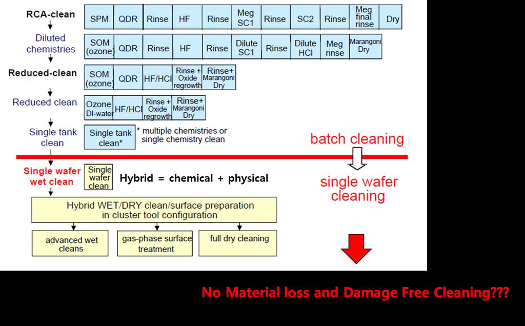
8 Cleaning sequences: roadmap 8
 - Organic Contamination removal and PR strip HF (+ H 2 O 2 ) : Last wet cleaning - HF : Native oxide and H 2 O 2 : Metal removal")
9 Traditional Wafer Cleaning Chemicals and Technology SC-1(NH 4 OH+H 2 O 2 +H 2 O=1:1:5 at 80 ~ 90 C) - Particles and organic contamination removal SC-2(HCl+H 2 O 2 +H 2 O=1:1:5) at 80 ~ 90 C ) - Trace and Noble Metal removal Piranha(H 2 SO 4 :H 2 O 2 =4:1 at 90 ~ 120 C) - Organic Contamination removal and PR strip HF (+ H 2 O 2 ) : Last wet cleaning - HF : Native oxide and H 2 O 2 : Metal removal Megasnic 9

10 Single Wafer Cleaning Technology 10


11 Single Wafer vs. Wet Bench Cleans Gates S/D Epi All Cleans on Wet Bench Overetched Hard Mask All Single Wafer Cleans Reduced overetch Improved Selectivity 11

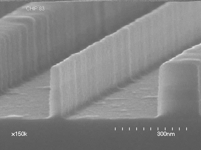
12 Cleaning of Fragile Structures 22 nm 30 nm 12

13 Cleaning without damages 13


14 Wafer Drying Technology Spin dryer DI water, liquid IPA, vapor IPA, hot IPA Marangoni IPA dryer 14

15 CMP Challenges in 10 nm/7 nm Number of CMP steps doubled from 28nm to 10nm node in order to enable new integration schemes such as replacement metal gate and self-aligned contact. ~ 75% of the increase is in MOL due to the complexity of contact module. New CMP processes such as Co, Cap SiN and SiOC CMP in MOL J. Han, CSTIC,


16 CMP Process for 3D FinFET -FEOL Critical CMP step in FEOP for sub-28 nm Replacement Metal Gate application (RMG) FinFET technology have been described STI CMP for bulk FinFET Fin formation Gate deposition Gate Planarization Gate patterning Ext. / HALO implant Spec on SiN : < 2nm variation WID/WIW Poly-open or ILD0 CMP Dummy gate removal Dummy dielectric removal IL-SiO 2 /HfO 2 deposition WF MG + Fill-in MG deposition MG CMP Spec on gate height variation : < 5nm variation WID/WIW Spacers formation HDD Si epi HDD implantation Anneal CESL and ILD0 deposition Thickness on Fin and on Field : <5 nm WID/WIW Spec on gate height variation : < 5nm variation WID/WIW Each CMP step has tight SPEC s in terms of WID and WIW uniformity control Continuous improvement ongoing towards smaller technology nodes *K. Devriendt, P. Ong, ICPT2012, *K. Devriendt, K. Kellens, A. Veloso, R. Athimulam, ICPT2011, p536 16


17 How do we clean polished wafers? PVA Brushes!! 17
 + Pencil Brush (Middle Particle) GF, SPCC")
18 Nano Particle Removal in Post CMP Cleaning Typical Brush (Large Particle) + Pencil Brush (Middle Particle) GF, SPCC


19 Defect Level of PVA Brush s Stage < Defect count vs. Time> [Initial] Break-in Process Laststage < Shear Force Vs. Time> Main Process - Initial > Last-stage >> Main Process *Ref: ITW Rippey Defect count is increased by brush cleaning in long run process. Shear force is decreased by brush cleaning in long run process. PVA brush cleaning performance decreases as a function of process time. 19

 SC-1")
 DHF Chemical by-product")


20 FE-SEM Analysis of Fully-Used PVA Brush New Brush 20 kx Post Tungsten CMP (Silica) DHF 20 kx Chemical by-product 2 µm 2 µm Post Oxide CMP (Silica) SC-1 Cleaning Post Oxide CMP (Silica) DHF Post Oxide CMP (Ceria) DHF Chemical by-product 20 kx Chemical by-product 20 kx Ceria particles with Chemical by-product 20 kx 2 µm 2 µm 2 µm Different types of slurry and cleaning chemistry affect contamination of brush surface. 20
21 Brush Treatment Methods with Different Chemicals # Method Solution ph Dipping (24 Hr) Scrubbing (12 Hr) DIW 7 DHF (0.9:100 = HF:DIW) SC-1 (1:2:40 = NH 4 OH:H 2 O 2 :DIW) DIW 7 DHF (0.9:100 = HF:DIW) SC-1 (1:2:40 = NH 4 OH:H 2 O 2 :DIW) Reference Condition 2 Types of Method : Dipping / Scrubbing 3 Types of Solution : DIW / SC-1 / DHF 21

22 3D-Profiler Analysis of Chemical Treated PVA Brushes DHF scrubbed PVA brush shows flattened surface. SC-1 scrubbed PVA brush shows rough surface. 22
23 3D-Profiler Analysis of Chemical Treated PVA Brushes Analyzed Surface Roughness of Various Chemical Treated PVA Brushes Dipping Scrubbing All dipped brushes show the similar morphology and surface roughness. The scrubbed brushes show significant change in morphology and surface roughness. It will affect the change of real contact area between brush and particles on wafer. DHF scrubbed PVA brush shows flattened surface with the lowest surface roughness. 23


24 FE-SEM Analysis of Chemical Treated PVA Brushes Initial 100 x 500 µm SC-1 Treated 100 x DHF Treated 100 x Removed skin layer Remained and Flattened skin layer 500 µm 500 µm SC-1 treated brush shows the removed skin layer. DHF treated brush shows remained and flattened skin layer. It will affect the final cleaning performance on wafers. 24
 (b) (c) (a) compressive stress measurement of various chemical treated brushes, (b) its magnified")

25 Compress Stress Analysis of Chemical Treated PVA Brushes D D S D D S (a) (b) (c) (a) compressive stress measurement of various chemical treated brushes, (b) its magnified region, (c) compressive strength A significant change of elastic property was observed in scrubbed brush when compared to the chemical dipped brush. The SC-1 treated brush showed more changes in its compressive stress than DHF treated brush. 25
26 Effect of Brush Treatment Methods and Chemicals Dipping Scrubbing Overall DHF SC-1 Surface morphology Similar Significant changes Flattened Rough Surface roughness value Similar Significant changes Lowest Skin layer Remained Significant changes Remained Removed Elastic property Similar Significant changes Lowest The scrubbed brushes show the significant changes in the morphology and surface roughness. The SC-1 treated brush shows more elastic and morphological changes than DHF treated brush. 26
 :")


27 CMP Process for High Mobility Channel Materials CMOS performance can be enhanced by using high-mobility channel materials - III/V materials (nmos) : high electron mobility / Ge (pmos) : high hole mobility - The approach followed in this work is Ge-STI approach Standard STI on bulk Si wafer Selective Si recess etch Selective epitaxial Ge growth on Si CMP of Ge stopping on SiO 2 Ge deposition After Ge CMP TDD reduction anneal CMP requirement - Good planarity - Low amount defects - Low surface roughness *P. Ong, C. Gillot, S. Ansar, B. Noller, Y. Li, L. Leunissen, ICPT2012, p23 *P. Ong, L. Witters, ICPT2010, p69 27


28 Low Defectivity III-V CMP Process Improving Defectivity for III-V CMP Processes for <10 nm Technology Nodes Hard Pad InP-filled structure Integration of III-V channels ART c Soft Pad Defect reduced SEM AFM InP in STI trenches can be removed by choosing the appropriate slurry/pad combination Hard Pad < Soft Pad Good surface achieved by using soft pad Not yet optimized on defect control on polished III-V surfaces InGaAs surface post CMP using soft pad *Lieve Teugels, Patrick Ong, Guillaume Boccardi, Niamh Waldron, ICPT2014, p15 28


29 Post InGaAs CMP Cleaning Issues of III-V post CMP cleaning InGaAs CMP using silica slurry Silica slurry abrasives were not removed perfectly after post CMP cleaning DIW megasonic followed by 2 brush steps with <1% diluted ammonia Need to selective cleaning of III-V surface Chemical cleaning : etching, electro-repulsion Physical cleaning Slurry Conditioner Pressure Carrier Post CMP cleaning After CMP process Silica After CMP process Silica slurry residue Polishing pad III-V SiO 2 29
30 InAs Etching Mechanism of SC-2 Etching mechanism according to the HCl concentration High concentration: oxidation rate < dissolution rate Low concentration : oxidation rate > dissolution rate In-As Slow step In-OH As-OH Fast step In-Cl As-Cl Stabilization Lower etch rate { InCl(OH) 2 } surf { AsCl(OH) 2 } surf Fast step Dissolution product { InCl n (3-n)+ } soln { AsCl n (3-n)+ } soln { In(OH) 3 } surf Fast step HCl : etching H 2 O 2 : oxidation -H 2 O : dehydration Destabilization Higher etch rate { As(OH) 3 } surf Oxidation product In 2 O 3 /As 2 O 3 Dennis H. Van Dorp, Sophia Arnauts, Frank Holsteyns and Stefan De Gendt, ECS Journal of Solid State Science and Technology, 4(6) N5061-N5066 (2015) 30
31 Defect Control Map Zero Defectivity (Defect Control) < CMP > < Post CMP Cleaning > Scratch (line, chatter) Corrosion Organic contamination Scratch (circular type) Particle Slurry, Pad Process condition Inhibitor Cleaning solution Inhibitor Process condition Brush characteristic Slurry & Pad development Effective inhibitor Easily removable inhibitor Brush study Or New technology Introduction of new inhibitors Understanding of brush characteristics Synergy between cleaning system and chemistry 31
32 Summary CMP becomes more importance in 1x nm below device design and fabrication CMP Challenges : FEOL, MOL process- defect sensitive New consumable and cleaning technology needed Current cleaning process and technology are available and could solve all contamination issues in post CMP cleaning 32


33
CMP challenges in sub-14nm FinFET and RMG technologies
 CMP challenges in sub-14nm FinFET and RMG technologies Tae Hoon Lee*, Hong Jin Kim, Venugopal Govindarajulu, Gerett Yocum & Jason Mazzotti Advanced Module Engineering NCCAVS CMPUG Spring Meeting 2016 Contents
Research Activities on Defect Improvement of CMP Process in 1x nm Foundry Device
 Research Activities on Defect Improvement of CMP Process in 1x nm Foundry Device 1JI CHUL YANG, 2Hong Jin Kim, 2Venu. Govindarajulu,1Dinesh Koli and 2Jason Mazzotti Jichul.yang@globalfoundries.com 1 CMP,
Cleaning Trends for Advanced Nodes. April 9, 2018 Scotten W. Jones President IC Knowledge LLC
 Cleaning Trends for Advanced Nodes April 9, 2018 Scotten W. Jones President IC Knowledge LLC sjones@icknowledge.com Outline DRAM Logic NAND Conclusion 2 DRAM Nodes 2011 2012 2013 2014 2015 2016 2017 2018
CMP Scratches; Their Detection and Analysis on Root Causes
 6 th LEVITRONIX CMP and Ultrapure Conference The Westin Park Central, Dallas, Texas May 11-12, 2011 CMP Scratches; Their Detection and Analysis on Root Causes Jin-Goo Park May 11, 2011 Department of Materials
Post Cleaning Chemical of Tungsten Chemical Mechanical Planarization for Memory Devices. Jun Yong Kim Cleaning/CMP Technology
 Post Cleaning Chemical of Tungsten Chemical Mechanical Planarization for Memory Devices Jun Yong Kim Cleaning/CMP Technology 1. CMP Process and Cleaning challenges 2. Problem Statement 3. Results of Cleaning
Process Optimization in Post W CMP In-situ Cleaning. Hong Jin Kim, Si-Gyung Ahn, Liqiao Qin CMP, Advanced Module Engineering GLOBALFOUNDRIES, USA
 Process Optimization in Post W CMP In-situ Cleaning Hong Jin Kim, Si-Gyung Ahn, Liqiao Qin CMP, Advanced Module Engineering GLOBALFOUNDRIES, USA Contents W CMP process for sub 14nm device W Gate CMP W
Czochralski Crystal Growth
 Czochralski Crystal Growth Crystal Pulling Crystal Ingots Shaping and Polishing 300 mm wafer 1 2 Advantage of larger diameter wafers Wafer area larger Chip area larger 3 4 Large-Diameter Wafer Handling
CMP COST ISSUES & IMPACT ON CONSUMABLES FOR MEMORY AND LOGIC
 CMP COST ISSUES & IMPACT ON CONSUMABLES FOR MEMORY AND LOGIC CMPUG @CNSE April 16, 2016 Mike Corbett Managing Partner mcorbett@linx-consulting.com Agenda INTRODUCTION TO LINX CONSULTING SEMI INDUSRTY OUTLOOK
CMOS Technology. Flow varies with process types & company. Start with substrate selection. N-Well CMOS Twin-Well CMOS STI
 CMOS Technology Flow varies with process types & company N-Well CMOS Twin-Well CMOS STI Start with substrate selection Type: n or p Doping level, resistivity Orientation, 100, or 101, etc Other parameters
CMP Defects and Evolution of PCMP Cleans
 CMP Defects and Evolution of PCMP Cleans March 27, 2017 Iqbal Ali iali@linx-consulting.com (408)839-9924 SPCC & PCMP Conference, Austin, TX Agenda 1. Introduction to Linx Consulting 2. Where Have We Been
April 11, th Surface Preparation and Cleaning Conference (SPCC) Department of 1 Bionanotechnology and 2
 Department of 1 Bionanotechnology and 2") 19 th Surface Preparation and Cleaning Conference (SPCC) April 11, 2018 Jung-Hwan Lee 1, Murhukrishnan Purushothaman 1, Kwang-Min Han 1, Shohei Shima 3, Satomi Hamada 3, Hirokuni Hiyama 3, and Jin-Goo
19 th Surface Preparation and Cleaning Conference (SPCC) April 11, 2018 Jung-Hwan Lee 1, Murhukrishnan Purushothaman 1, Kwang-Min Han 1, Shohei Shima 3, Satomi Hamada 3, Hirokuni Hiyama 3, and Jin-Goo
CMP Solutions for 10nm and Beyond: Breaking trade-offs in the Planarization / Defect Balance
 SMC Korea May 18, 2016 CMP Solutions for 10nm and Beyond: Breaking trade-offs in the Planarization / Defect Balance Marty W. DeGroot Global R&D Director, CMP Technologies, The Dow Chemical Company Key
New Materials as an enabler for Advanced Chip Manufacturing
 New Materials as an enabler for Advanced Chip Manufacturing Drive Innovation, Deliver Excellence ASM International Analyst and Investor Technology Seminar Semicon West July 10 2013 Outline New Materials:
Simple Cubic Crystal
 Starting Material Simple Cubic Crystal Crystal Planes offset by d/4 Diamond lattice cell (C, Si, Ge, etc.) face atom in FCC corner atom in FCC (100) plane (110) plane (111) plane Crystal Planes/Direction
Study of cobalt etching speed controling by ph and oxidizer concentraion
 Study of cobalt etching speed controling by ph and oxidizer concentraion Kurita Water Industries Ltd. Yuichi Ogawa, Nobuko Gan, Toru Masaoka, Minami Yoshimura, Hideaki Iino imec vzw Quoc Toan Le, Els Kesters,
The ABC s of CMP for DWB and SOI. Robert L. Rhoades, Ph.D. CAMP Conference Presentation August 9, 2010
 The ABC s of CMP for DWB and SOI Robert L. Rhoades, Ph.D. CAMP Conference Presentation August 9, 2010 Outline Introduction Direct Wafer Bonding (DWB) Background CMP for DWB Silicon-On-Insulator (SOI) Background
Nonplanar Metallization. Planar Metallization. Professor N Cheung, U.C. Berkeley
 Nonplanar Metallization Planar Metallization Passivation Metal 5 (copper) Metal 3 (copper) Interlevel dielectric (ILD) Via (tungsten) Metal 1 (copper) Tungsten Plug to Si Silicon Caps and Plugs oxide oxide
Enabling Low Defectivity Solutions Through Co- Development of CMP Slurries and Cleaning Solutions for Cobalt Interconnect Applications
 Enabling Low Defectivity Solutions Through Co- Development of CMP Slurries and Cleaning Solutions for Cobalt Interconnect Applications Dnyanesh Tamboli 1, Tom Shi 1, Chris Li 2, Ming-Shih Tsai 2, Rung-Je
CONTROLLED COBALT RECESS FOR ADVANCED INTERCONNECT METALLIZATION.
 CONTROLLED COBALT RECESS FOR ADVANCED INTERCONNECT METALLIZATION. Antoine Pacco a *, Y. Akanishi b, Q.T. Le a, E. Kesters a, G. Murdoch a, F. Holsteyns a A IMEC VZW, KAPELDREEF 75, 3001 LEUVEN, BELGIUM
Post CMP Defects; Their Origin and Removal
 2007 Levitronix CMP Users Conference Post CMP Defects; Their Origin and Removal Jin-Goo Park Div. of Materials and Chemical Engineering, Hanyang University, Ansan 426-791, Korea February 15, 2007 KOTEF
Post-CMP Cleaning: Interaction between Particles and Surfaces
 Post-CMP Cleaning: Interaction between Particles and Surfaces J.-G. Park and T.-G. Kim Department of Materials Engineering, Hanyang University, Ansan, 426-791, South Korea E-mail: jgpark@hanyang.ac.kr
EE 330 Lecture 9. IC Fabrication Technology Part 2
 EE 330 Lecture 9 IC Fabrication Technology Part 2 Quiz 8 A 2m silicon crystal is cut into wafers using a wire saw. If the wire diameter is 220um and the wafer thickness is 350um, how many wafers will this
Microstructure of Electronic Materials. Amorphous materials. Single-Crystal Material. Professor N Cheung, U.C. Berkeley
 Microstructure of Electronic Materials Amorphous materials Single-Crystal Material 1 The Si Atom The Si Crystal diamond structure High-performance semiconductor devices require defect-free crystals 2 Crystallographic
ECSE 6300 IC Fabrication Laboratory Lecture 8 Metallization. Die Image
 ECSE 6300 IC Fabrication Laboratory Lecture 8 Metallization Prof. Rensselaer Polytechnic Institute Troy, NY 12180 Office: CII-6229 Tel.: (518) 276-2909 e-mails: luj@rpi.edu http://www.ecse.rpi.edu/courses/s18/ecse
EE 330 Lecture 9. IC Fabrication Technology Part II. -Oxidation -Epitaxy -Polysilicon -Planarization -Resistance and Capacitance in Interconnects
 EE 330 Lecture 9 IC Fabrication Technology Part II -Oxidation -Epitaxy -Polysilicon -Planarization -Resistance and Capacitance in Interconnects Review from Last Time Etching Dry etch (anisotropic) SiO
POST-CMP CLEANING OF HYDROPHILIC AND HYDROPHOBIC FILMS USING AQUEOUS ASSISTED CO 2 CRYOGENIC CLEANING
 POST-CMP CLEANING OF HYDROPHILIC AND HYDROPHOBIC FILMS USING AQUEOUS ASSISTED CO 2 CRYOGENIC CLEANING Souvik Banerjee, Andrea Via and Harlan F. Chung EcoSnow Systems Inc. Livermore, CA Robert Small and
EE40 Lec 22. IC Fabrication Technology. Prof. Nathan Cheung 11/19/2009
 Suggested Reading EE40 Lec 22 IC Fabrication Technology Prof. Nathan Cheung 11/19/2009 300mm Fab Tour http://www-03.ibm.com/technology/manufacturing/technology_tour_300mm_foundry.html Overview of IC Technology
THE IMPACT OF 3D DEVICES ON THE FUTURE OF PROCESS MATERIALS TRENDS & OPPORTUNITIES
 THE IMPACT OF 3D DEVICES ON THE FUTURE OF PROCESS MATERIALS TRENDS & OPPORTUNITIES L. Shon Roy K. Holland, PhD. October 2014 Materials Examples Process materials used to make semiconductor devices Gases
Linx Consulting Inc. CMP TECHNOLOGIES and MARKETS to the 5 nm NODE. See Beyond the Horizon. Eighth Edition
 See Beyond the Horizon Linx Consulting Inc. Pu b l i s h e d 3 Q 2 0 1 8 CMP TECHNOLOGIES and MARKETS to the 5 nm NODE Eighth Edition Uncertainty around true materials requirements is a huge risk for leading
Lecture 2: CMOS Fabrication Mark McDermott Electrical and Computer Engineering The University of Texas at Austin
 Lecture 2: CMOS Fabrication Mark McDermott Electrical and Computer Engineering The University of Texas at Austin Agenda Last module: Introduction to the course How a transistor works CMOS transistors This
Overview of Dual Damascene Cu/Low-k Interconnect
 ERC Retreat Stanford: New Chemistries & Tools for scco 2 Processing of Thin Films Overview of Dual Damascene Cu/Low-k Interconnect P. Josh Wolf 1,4 - Program Manager, Interconnect Div. josh.wolf@sematech.org
EE 330 Lecture 9. IC Fabrication Technology Part II. -Oxidation -Epitaxy -Polysilicon -Planarization -Resistance and Capacitance in Interconnects
 EE 330 Lecture 9 IC Fabrication Technology Part II -Oxidation -Epitaxy -Polysilicon -Planarization -Resistance and Capacitance in Interconnects Review from Last Time IC Fabrication Technology Crystal Preparation
UT Austin, ECE Department VLSI Design 2. CMOS Fabrication, Layout Rules
 2. CMOS Fabrication, Layout, Design Rules Last module: Introduction to the course How a transistor works CMOS transistors This module: CMOS Fabrication Design Rules CMOS Fabrication CMOS transistors are
CMP Solutions for the Integration of High-K Metal Gate Technologies
 CMP Solutions for the Integration of High-K Metal Gate Technologies J. M.. Dysard, V. Brusic, P. Feeney, S. Grumbine, K. Moeggenborg, G. Whitener, W. J. Ward, G. Burns, and K. Choi Cabot Microelectronics
Lect. 2: Basics of Si Technology
 Unit processes Thin Film Deposition Etching Ion Implantation Photolithography Chemical Mechanical Polishing 1. Thin Film Deposition Layer of materials ranging from fractions of nanometer to several micro-meters
Tri-Gate Transistor Architecture with High-k Gate Dielectrics, Metal Gates and Strain Engineering
 Tri-Gate Transistor Architecture with High-k Gate Dielectrics, Metal Gates and Strain Engineering Jack Kavalieros, Brian Doyle, Suman Datta, Gilbert Dewey, Mark Doczy, Ben Jin, Dan Lionberger, Matthew
CMOS FABRICATION. n WELL PROCESS
 CMOS FABRICATION n WELL PROCESS Step 1: Si Substrate Start with p- type substrate p substrate Step 2: Oxidation Exposing to high-purity oxygen and hydrogen at approx. 1000 o C in oxidation furnace SiO
Chapter 4 : ULSI Process Integration (0.18 m CMOS Process)
") Chapter : ULSI Process Integration (0.8 m CMOS Process) Reference. Semiconductor Manufacturing Technology : Michael Quirk and Julian Serda (00). - (00). Semiconductor Physics and Devices- Basic Principles(/e)
Chapter : ULSI Process Integration (0.8 m CMOS Process) Reference. Semiconductor Manufacturing Technology : Michael Quirk and Julian Serda (00). - (00). Semiconductor Physics and Devices- Basic Principles(/e)
INTEGRATED-CIRCUIT TECHNOLOGY
 INTEGRATED-CIRCUIT TECHNOLOGY 0. Silicon crystal growth and wafer preparation 1. Processing Steps 1.1. Photolitography 1.2. Oxidation 1.3. Layer Deposition 1.4. Etching 1.5. Diffusion 1.6 Backend: assembly,
Wet Processing Techniques for Achieving Ultra-shallow Junctions in Future CMOS Devices
 Accelerating the next technology revolution Wet Processing Techniques for Achieving Ultra-shallow Junctions in Future CMOS Devices Joel Barnett, Richard Hill, Chris Hobbs and Prashant Majhi 07-October-2010
Review of CMOS Processing Technology
 - Scaling and Integration Moore s Law Unit processes Thin Film Deposition Etching Ion Implantation Photolithography Chemical Mechanical Polishing 1. Thin Film Deposition Layer of materials ranging from
Complementary Metal Oxide Semiconductor (CMOS)
") Technische Universität Graz Institute of Solid State Physics Complementary Metal Oxide Semiconductor (CMOS) Franssila: Chapters 26,28 Technische Universität Graz Institute of Solid State Physics Complementary
Technische Universität Graz Institute of Solid State Physics Complementary Metal Oxide Semiconductor (CMOS) Franssila: Chapters 26,28 Technische Universität Graz Institute of Solid State Physics Complementary
ECE321 Electronics I
 ECE321 Electronics I Lecture 19: CMOS Fabrication Payman Zarkesh-Ha Office: ECE Bldg. 230B Office hours: Tuesday 2:00-3:00PM or by appointment E-mail: payman@ece.unm.edu Slide: 1 Miller Effect Interconnect
CMOS Manufacturing process. Design rule set
 CMOS Manufacturing process Circuit design Set of optical masks Fabrication process Circuit designer Design rule set Process engineer All material: Chap. 2 of J. Rabaey, A. Chandrakasan, B. Nikolic, Digital
EE 434 Lecture 9. IC Fabrication Technology
 EE 434 Lecture 9 IC Fabrication Technology Quiz 7 The layout of a film resistor with electrodes A and B is shown. If the sheet resistance of the film is 40 /, determine the resistance between nodes A and
MICROCHIP MANUFACTURING by S. Wolf
 MICROCHIP MANUFACTURING by S. Wolf Chapter 8: CONTAMINATION- CONTROL & CLEANING TECHNOLOGY for ULSI APPLICATIONS 2004 by LATTICE PRESS CHAPTER CONTENTS Contamination-Types in IC Fabrication Sources of
Integration Issues with Cu CMP
 Integration Issues with Cu CMP Copper CMP Integrated Solutions Michael R. Oliver Rodel, Inc. December 3, 2003 Outline Dual Damascene Approach Requirements Impact of Cu Deposition Topography Issues Sensitivity
Integrated Circuits & Systems
 Federal University of Santa Catarina Center for Technology Computer Science & Electronics Engineering Integrated Circuits & Systems INE 5442 Lecture 6 CMOS Fabrication Process & Design Rules guntzel@inf.ufsc.br
Copper Interconnect Technology
 Tapan Gupta Copper Interconnect Technology i Springer Contents 1 Introduction 1 1.1 Trends and Challenges 2 1.2 Physical Limits and Search for New Materials 5 1.3 Challenges 6 1.4 Choice of Materials 7
Emerging Materials for Front End IC Process
 Emerging Materials for Front End IC Process Mark Thirsk Linx Consulting +1 617 273 8837 mthirsk@linx-consulting.com Device Making Unit Operations - 2007 100% 0.065 Total = 12,229,682 80 0.09 60 40 0.13
Lecture 030 Integrated Circuit Technology - I (5/8/03) Page 030-1
 Page 030-1") Lecture 030 Integrated Circuit Technology - I (5/8/03) Page 030-1 LECTURE 030 INTEGRATED CIRCUIT TECHNOLOGY - I (References [7,8]) Objective The objective of this presentation is: 1.) Illustrate integrated
Lecture 030 Integrated Circuit Technology - I (5/8/03) Page 030-1 LECTURE 030 INTEGRATED CIRCUIT TECHNOLOGY - I (References [7,8]) Objective The objective of this presentation is: 1.) Illustrate integrated
Make sure the exam paper has 9 pages total (including cover page)
") UNIVERSITY OF CALIFORNIA College of Engineering Department of Electrical Engineering and Computer Sciences Fall 2010 EE143 Midterm Exam #2 Family Name First name SID Signature Solution Make sure the exam
UNIVERSITY OF CALIFORNIA College of Engineering Department of Electrical Engineering and Computer Sciences Fall 2010 EE143 Midterm Exam #2 Family Name First name SID Signature Solution Make sure the exam
CMP Process Development for the Via- Middle 3D TSV Applications at 28nm Technology Node
 CMP Process Development for the Via- Middle 3D TSV Applications at 28nm Technology Node UMC/ ATD_AM / CMP Department T. C. Tsai, W. C. Tsao, Welch Lin, C. L. Hsu, C. L. Lin, C. M. Hsu, J. F. Lin, C. C.
Cost of Integrated Circuits
 Cost of IC Design 1 Cost of Integrated Circuits NRE (Non-Recurrent Engineering) costs fixed design time and effort, mask generation independent of sales volume / number of products one-time cost factor
Chapter 2 Manufacturing Process
 Digital Integrated Circuits A Design Perspective Chapter 2 Manufacturing Process 1 CMOS Process 2 CMOS Process (n-well) Both NMOS and PMOS must be built in the same silicon material. PMOS in n-well NMOS
EE CMOS TECHNOLOGY- Chapter 2 in the Text
 1 EE 212 FALL 1999-00 CMOS TECHOLOGY- Chapter 2 in the Text In this set of notes we will describe a modern CMOS process flow. In the simplest CMOS technologies, we need to realize simply MOS and MOS transistors
VLSI Systems and Computer Architecture Lab
 ΚΥΚΛΩΜΑΤΑ VLSI Πανεπιστήμιο Ιωαννίνων CMOS Technology Τμήμα Μηχανικών Η/Υ και Πληροφορικής 1 From the book: An Introduction ti to VLSI Process By: W. Maly ΚΥΚΛΩΜΑΤΑ VLSI Διάρθρωση 1. N well CMOS 2. Active
OXIDE STOP-IN-FILM CMP: NEW CHALLENGES FOR THE NEXT GENERATION MEMORY DEVICES. Andrey Zagrebelny, Sony Varghese, Andrew Carswell
 OXIDE STOP-IN-FILM CMP: NEW CHALLENGES FOR THE NEXT GENERATION MEMORY DEVICES Andrey Zagrebelny, Sony Varghese, Andrew Carswell 1 INTRODUCTION ITRS roadmap: Moore s Law vs. 3D/vertical architectures New
CMOS Processing Technology
 CHAPTER 2 CMOS Processing Technology Outline 2 1. CMOS Technologies 2. Layout Design Rules 3. CMOS Process Enhancements 4. Technology-related CAD Issues 5. Manufacturing Issues CMOS Technologies 3 n-well
9/4/2008 GMU, ECE 680 Physical VLSI Design
 ECE680: Physical VLSI Design Chapter II CMOS Manufacturing Process 1 Dual-Well Trench-Isolated CMOS Process gate-oxide TiSi 2 AlCu Tungsten SiO 2 p-well poly n-well SiO 2 n+ p-epi p+ p+ 2 Schematic Layout
CMOS Processing Technology
 CHAPTER 2 CMOS Processing Technology Outline 2 1. CMOS Technologies 2. Layout Design Rules 3. CMOS Process Enhancements 4. Technology-related CAD Issues 5. Manufacturing Issues CMOS Technologies 3 n-well
Lecture #18 Fabrication OUTLINE
 Transistors on a Chip Lecture #18 Fabrication OUTLINE IC Fabrication Technology Introduction the task at hand Doping Oxidation Thin-film deposition Lithography Etch Lithography trends Plasma processing
PROCESS FLOW AN INSIGHT INTO CMOS FABRICATION PROCESS
 Contents: VI Sem ECE 06EC63: Analog and Mixed Mode VLSI Design PROCESS FLOW AN INSIGHT INTO CMOS FABRICATION PROCESS 1. Introduction 2. CMOS Fabrication 3. Simplified View of Fabrication Process 3.1 Alternative
Isolation Technology. Dr. Lynn Fuller
 ROCHESTER INSTITUTE OF TECHNOLOGY MICROELECTRONIC ENGINEERING Isolation Technology Dr. Lynn Fuller Motorola Professor 82 Lomb Memorial Drive Rochester, NY 14623-5604 Tel (585) 475-2035 Fax (585) 475-5041
CMP for Thru-Silicon Vias TSV Overview & Examples March 2009
 CMP for Thru-Silicon Vias TSV Overview & Examples March 2009 Packaging Evolution Source: Yole Dev 2007 2 3D Integration Source: Yole Dev 2007 Growth rates for 3D integration Flash continues to drive the
VLSI INTRODUCTION P.VIDYA SAGAR ( ASSOCIATE PROFESSOR) Department of Electronics and Communication Engineering, VBIT
 Department of Electronics and Communication Engineering, VBIT") VLSI INTRODUCTION P.VIDYA SAGAR ( ASSOCIATE PROFESSOR) contents UNIT I INTRODUCTION: Introduction to IC Technology MOS, PMOS, NMOS, CMOS & BiCMOS technologies. BASIC ELECTRICAL PROPERTIES : Basic Electrical
VLSI INTRODUCTION P.VIDYA SAGAR ( ASSOCIATE PROFESSOR) contents UNIT I INTRODUCTION: Introduction to IC Technology MOS, PMOS, NMOS, CMOS & BiCMOS technologies. BASIC ELECTRICAL PROPERTIES : Basic Electrical
Linx Consulting, Inc.
 STRATEGIC COST MODEL A Collaborative Development between Linx Consulting and IC Knowledge Background Based on real world product process flows and device roadmaps, with modifications for the latest process
EE 143 CMOS Process Flow
 EE 143 CMOS rocess Flow CT 84 D D G Sub G Sub S S G D S G D S + + + + - MOS Substrate Well - MOS Substrate EE 143 CMOS rocess Flow CT 85 hotoresist Si 3 4 SiO 2 Substrate selection: moderately high resistivity,
1.1 Background Cu Dual Damascene Process and Cu-CMP
 Chapter I Introduction 1.1 Background 1.1.1 Cu Dual Damascene Process and Cu-CMP In semiconductor manufacturing, we always directed toward adding device speed and circuit function. Traditionally, we focused
ELEC 7364 Lecture Notes Summer Si Oxidation. by STELLA W. PANG. from The University of Michigan, Ann Arbor, MI, USA
 ELEC 7364 Lecture Notes Summer 2008 Si Oxidation by STELLA W. PANG from The University of Michigan, Ann Arbor, MI, USA Visiting Professor at The University of Hong Kong The University of Michigan Visiting
SKW Wafer Product List
 SKW Wafer Product List Regularly updated (2.13.2018) SKW Associates, INC. 2920 Scott Blvd, Santa Clara, CA 95054 Tel: 408-919-0094, Fax: 408-919-0097 I. Available Wafers in 200mm and 300mm - Please refer
EE 330 Lecture 8. IC Fabrication Technology Part II. - Oxidation - Epitaxy - Polysilicon - Interconnects
 EE 330 Lecture 8 IC Fabrication Technology Part II - Oxidation - Epitaxy - Polysilicon - Interconnects Review from Last Time MOS Transistor Bulk Source Gate Drain p-channel MOSFET Lightly-doped n-type
Chapter 4. UEEP2613 Microelectronic Fabrication. Oxidation
 Chapter 4 UEEP2613 Microelectronic Fabrication Oxidation Prepared by Dr. Lim Soo King 24 Jun 2012 Chapter 4...113 Oxidation...113 4.0 Introduction... 113 4.1 Chemistry of Silicon Dioxide Formation... 115
Lecture 3. Wafer Clean and Wet Processing
 Lecture 3 Wafer Clean and Wet Processing Lecture 2: Wafer Fabrication and Silicon Epitaxy Recap Wafer Fabrication Czochralski (CZ) Method Float Zone (FZ) Method From Ingot to Wafer Gettering Silicon-on-Insulator
Lecture 22: Integrated circuit fabrication
 Lecture 22: Integrated circuit fabrication Contents 1 Introduction 1 2 Layering 4 3 Patterning 7 4 Doping 8 4.1 Thermal diffusion......................... 10 4.2 Ion implantation.........................
EE 143 MICROFABRICATION TECHNOLOGY FALL 2014 C. Nguyen PROBLEM SET #9
 Issued: Tuesday, Nov. 11, 2014 PROBLEM SET #9 Due: Wednesday, Nov. 19, 2010, 8:00 a.m. in the EE 143 homework box near 140 Cory 1. The following pages comprise an actual pwell CMOS process flow with poly-to-poly
CS/ECE 5710/6710. N-type Transistor. N-type from the top. Diffusion Mask. Polysilicon Mask. CMOS Processing
 CS/ECE 5710/6710 CMOS Processing Addison-Wesley N-type Transistor D G +Vgs + Vds S N-type from the top i electrons - Diffusion Mask Mask for just the diffused regions Top view shows patterns that make
Semiconductor Manufacturing Technology. Semiconductor Manufacturing Technology
 Semiconductor Manufacturing Technology Michael Quirk & Julian Serda October 2001 by Prentice Hall Chapter 10 Oxidation 2001 2000 by Prentice Hall Diffusion Area of Wafer Fabrication Wafer fabrication (front-end)
Oxidation SMT Yau - 1
 Oxidation Yau - 1 Objectives After studying the material in this chapter, you will be able to: 1. Describe an oxide film for semiconductor manufacturing, including its atomic structure, how it is used
Lecture 0: Introduction
 Lecture 0: Introduction Introduction Integrated circuits: many transistors on one chip. Very Large Scale Integration (VLSI): bucketloads! Complementary Metal Oxide Semiconductor Fast, cheap, low power
Introduction to CMOS VLSI Design. Layout, Fabrication, and Elementary Logic Design
 Introduction to CMOS VLSI Design Layout, Fabrication, and Elementary Logic Design CMOS Fabrication CMOS transistors are fabricated on silicon wafer Lithography process similar to printing press On each
Progress in Monolithic III-V/Si and towards processing III-V Devices in Silicon Manufacturing. E.A. (Gene) Fitzgerald
 Fitzgerald") Progress in Monolithic III-V/Si and towards processing III-V Devices in Silicon Manufacturing E.A. (Gene) Fitzgerald M.J. Mori, C.L.Dohrman, K. Chilukuri MIT Cambridge, MA USA Funding: MARCO IFC and Army
Progress in Monolithic III-V/Si and towards processing III-V Devices in Silicon Manufacturing E.A. (Gene) Fitzgerald M.J. Mori, C.L.Dohrman, K. Chilukuri MIT Cambridge, MA USA Funding: MARCO IFC and Army
Microelettronica. Planar Technology for Silicon Integrated Circuits Fabrication. 26/02/2017 A. Neviani - Microelettronica
 Microelettronica Planar Technology for Silicon Integrated Circuits Fabrication 26/02/2017 A. Neviani - Microelettronica Introduction Simplified crosssection of an nmosfet and a pmosfet Simplified crosssection
SLURRY FORMULATION OPTIONS
 SLURRY FORMULATION OPTIONS CHALLENGES FOR DEFECT REDUCTION IN CU,Ta/TaN AND Ru PLANARIZATION S. V. Babu Center for Advanced Materials Processing, 1 Clarkson University (www.clarkson.edu/camp) Acknowledgments
Chemical/Mechanical Balance Management through Pad Microstructure in Si CMP
 Chemical/Mechanical Balance Management through Pad Microstructure in Si CMP Post CMP Cleaning Austin 2017 Ratanak Yim (Viorel Balan) R. Yim 1,2,5, C. Perrot 2, V. Balan 1, P-Y. Friot 3, B. Qian 3, N. Chiou
EE C245 ME C218 Introduction to MEMS Design
 EE C245 ME C218 Introduction to MEMS Design Fall 2007 Prof. Clark T.-C. Nguyen Dept. of Electrical Engineering & Computer Sciences University of California at Berkeley Berkeley, CA 94720 Lecture 10: Surface
Overview of CMP for TSV Applications. Robert L. Rhoades, Ph.D. Presentation for AVS Joint Meeting June 2013 San Jose, CA
 Overview of CMP for TSV Applications Robert L. Rhoades, Ph.D. Presentation for AVS Joint Meeting June 2013 San Jose, CA Outline TSV s and the Role of CMP TSV Pattern and Fill TSV Reveal (non-selective)
EE 143 FINAL EXAM NAME C. Nguyen May 10, Signature:
 INSTRUCTIONS Read all of the instructions and all of the questions before beginning the exam. There are 5 problems on this Final Exam, totaling 143 points. The tentative credit for each part is given to
Feature-level Compensation & Control. CMP September 15, 2005 A UC Discovery Project
 Feature-level Compensation & Control CMP September 15, 2005 A UC Discovery Project Chemical Mechanical Planarization - Faculty Team Mechanical Phenomena David A. Dornfeld Mechanical Engineering UCB Fiona
FABRICATION of MOSFETs
 FABRICATION of MOSFETs CMOS fabrication sequence -p-type silicon substrate wafer -creation of n-well regions for pmos transistors, -impurity implantation into the substrate. -thick oxide is grown in the
2009 Market Slurries and Particles in CMP & a Bit Beyond
 2009 Market Slurries and Particles in CMP & a Bit Beyond NCCAVS CMPUG Semicon W Meeting Karey Holland, Ph.D. July 14, 2009 Techcet Group, LLC. KHolland@Techcet.com www.techcet.com Slurries & Particles
Doping and Oxidation
 Technische Universität Graz Institute of Solid State Physics Doping and Oxidation Franssila: Chapters 13,14, 15 Peter Hadley Technische Universität Graz Institute of Solid State Physics Doping Add donors
Hafnium -based gate dielectrics for high performance logic CMOS applications
 Hafnium -based gate dielectrics for high performance logic CMOS applications T. Kelwing*, M. Trentzsch, A. Naumann, B. Bayha, B. Trui, L. Herrmann, F. Graetsch, R. Carter, R. Stephan, P. Kuecher & W. Hansch
CyMOS process Spring 2016 Iowa State University
 CyMOS process Spring 2016 Iowa State University Start Date Starting Material Orientation: Dopant: Resistivity: Ω cm Doping Concentration: cm 3 Diameter: inch Thickness: µm Lot Identification: Wafer Count
Chapter 5 Thermal Processes
 Chapter 5 Thermal Processes 1 Topics Introduction Hardware Oxidation Diffusion Annealing Post-Implantation Alloying Reflow High Temp CVD Epi Poly Silicon Nitride RTP RTA RTP Future Trends 2 Definition
FRONT END PROCESSES - CLEANING, LITHOGRAPHY, OXIDATION ION IMPLANTATION, DIFFUSION, DEPOSITION AND ETCHING
 Manufacturing, Cleaning, Gettering - Chapter 4 FRONT END PROCESSES - CLEANING, LITHOGRAPHY, OXIDATION ION IMPLANTATION, DIFFUSION, DEPOSITION AND ETCHING Over the next several weeks, we ll study front
TSV Processing and Wafer Stacking. Kathy Cook and Maggie Zoberbier, 3D Business Development
 TSV Processing and Wafer Stacking Kathy Cook and Maggie Zoberbier, 3D Business Development Outline Why 3D Integration? TSV Process Variations Lithography Process Results Stacking Technology Wafer Bonding
Chapter 3 Silicon Device Fabrication Technology
 Chapter 3 Silicon Device Fabrication Technology Over 10 15 transistors (or 100,000 for every person in the world) are manufactured every year. VLSI (Very Large Scale Integration) ULSI (Ultra Large Scale
Cu CMP: Macro-scale Manufacturing for Nano-scale Quality Requirements
 Cu CMP: Macro-scale Manufacturing for Nano-scale Quality Requirements Jung-Hoon Chun Laboratory for Manufacturing and Productivity Massachusetts Institute of Technology Cambridge, MA 02139 April 23, 2009
Lecture 1A: Manufacturing& Layout
 Introduction to CMOS VLSI Design Lecture 1A: Manufacturing& Layout David Harris Harvey Mudd College Spring 2004 Steven Levitan Fall 2008 1 The Manufacturing Process For a great tour through the IC manufacturing