Microelectronics Packaging. Microsystems Packaging
|
|
|
- Todd Logan
- 6 years ago
- Views:
Transcription

1 Microelectronics Packaging Microsystems Packaging 1
2 Integration of IC, Packaging and System Packaging Hierarchy 2
3 System Packaging Technologies Summary of Microsystems Packaging 3
4 Moore s Law Evolution of the Microprocessor 4
5 IC Packaging Requirements Protect circuit from external environment Mechanical interface to PCB Interface for production testing Good signal transfer between chip and PCB Good power supply to IC Cooling Through-hole and Surface Mount Packages 5
6 Integrated Circuit Packaging Different applications have different requirements Logic (Microprocessors, ASIC s) High power, I/O count Small number per board (ok if bigger) Relatively high Average Selling Price (ASP) Memory (DRAM, Flash) Lower power and fewer I/O s per die Large number per board IC Package Types 6
7 Traditional IC Package Types Dual-in-line (DIP) 7


8 Quad Flat Pack (QFP) Wire Bond package Leads are coplanar fanning into die - higher coupling New IC Package Types 8
 Packages is same size as die Very space efficient Very short leads good electrical properties Back side of die exposed good")
9 Ball Grid Array (BGA) Most popular ASIC package Basically a small printed circuit board Create a 2-D array of pins under the package Multiple planes available in package Possible to route larger numbers of signals Better signal integrity Chip Scale Packages (CSP) Packages is same size as die Very space efficient Very short leads good electrical properties Back side of die exposed good thermal properties Possible to fabricate at wafer level 9

10 New IC Package Types Number of I/Os in a Package N KM p Rent s Rule N: number of pins or terminals K: average number of terminals per logic circuit M: number of circuits/gates P: Rent s constant 10
11 Rent s Constants System or Chip Type P K Static Memory Microprocessor Gate Array High Speed Computer Chip/module level Board / System level Terminals vs Number of Circuits 11
12 I/Os of a Chip For a 64MB Static RAM chip, signal I/Os of this chip is N SRAM 6 ( ) For a gate array chip with 5000 gates, signal I/Os of this chip is N gatearray Packaging Trend 12


13 IC Packaging Efficiency Technology Trend in IC Packaging Source: ERSO/ITRI 13

14 Bottlenecks & Break Through Solutions Source: ERSO/ITRI SHARP s 3-D System in Package 14
 (Cont.")
")
15 Multi-chip Module (MCM) Multi-chip Module (Cont.) SP5MX1 Pentium Module (43mm x 43mm) 15


16 Schematic Overview of SP5MX1 Cooling for MCM 16

17 Thermal Conduction Module (TCM) Source: IBM Three Types of MCM MCM-L MCM-C MCM-D 17

 63 18")
18 MCM-L Source: JOHNS HOPKINS APL TECHNICAL DIGEST, VOLUME 20, NUMBER 1 (1999) 63 MCM-C Source: JOHNS HOPKINS APL TECHNICAL DIGEST, VOLUME 20, NUMBER 1 (1999) 63 18
 63 Signal and Power Distribution for")
19 MCM-D Source: JOHNS HOPKINS APL TECHNICAL DIGEST, VOLUME 20, NUMBER 1 (1999) 63 Signal and Power Distribution for MCM 19
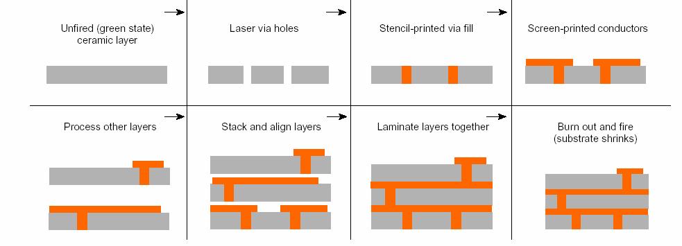
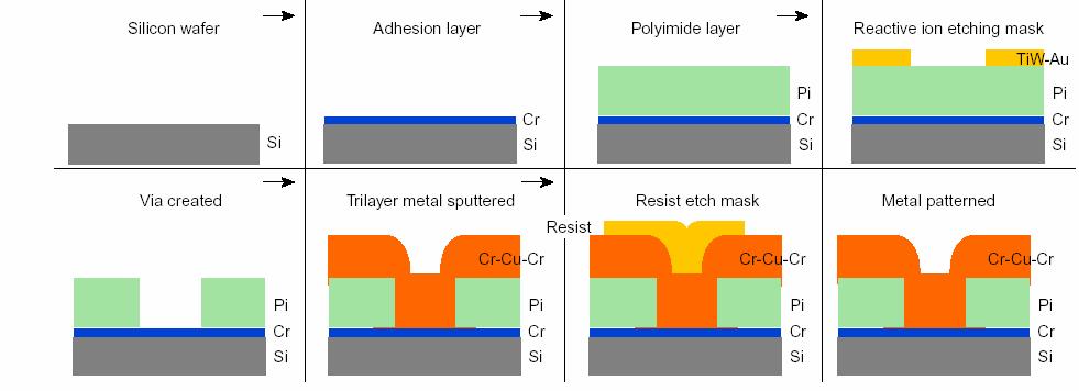
20 Fabrication of MCM-C Fabrication of MCM-D 20
21 MCM-L Substrate Structure Ni/Au solder resist metal 1 metal 2 core (FR4/5) prepregs metal 3 metal 4 drilled via (buried) micro via Source: Cork Institute of Technology PCB Laminate Materials NEMA Grade FR-2 FR-3 FR-4 FR-5 FR-6 CEM-1 CEM-3 Resin System Phenolic Epoxy Epoxy Epoxy Polyester Epoxy Epoxy Reinforcement Paper Paper Woven glass Woven glass Glass matte Paper and glass Woven glass and glass matte Description Punchable, flame resistant Flame resistant, high insulation resistance Flame resistance, Tg ~ 130C Flame resistant, higher Tg, better thermal Flame resistant, low capacitance or high impact applications Paper core and glass surface, selfextinguishing, excellent punching, longer drill life and minimal dust. Nonwoven glass core and woven glass surface, similar to FR-4, longer drill life 21

 63 Chip Scale Package")
22 Comparison of MCM Source: JOHNS HOPKINS APL TECHNICAL DIGEST, VOLUME 20, NUMBER 1 (1999) 63 Chip Scale Package (CSP) 22
 Market is the")

 System In")
23 System in Package (SIP) Wireless (RF) Market is the Key Driver Motorola, Philips LTCC is the Substrate of Choice CBGA Package SiP is not SOC (System On Chip) System In Package (Cont.) 23

24 Advantages of SIP over SOC RF IC s s Typically Take Manufacturing Passes Total Cost of Up To 5 Million Dollars 66 Month Impact to Schedule SIP on LTCC Total Cost Less Than 500K for Manufacturing Passes 66 Week Impact to Schedule Mixed Technology Support CMOS, GaAs, SiGe all on One Substrate Flexible Design Partitioning Bluetooth Standard Platform LTCC Process 24
")
 Tape-automated")
25 Applications for LTCC Bonding Methodologies (a) Wire bonding (b) Flip-chip bonding (c) Tape-automated bonding 25

26 Wire Bonding Pads are placed in one or two rows Logic devices Around periphery of die 1 row: 70μ pitch 2 rows: 40-50μ staggered pitch Memory (DRAM) in a line at center of die 1 row: μ pitch Wire Bonding Oldest attachment method and still dominant for ICs Au or Al wires are attached between pads and substrate using Thermocompression bonding Ultrasonic bonding Thermosonic bonding The process is time-consuming since each wire must be attached individually 26
 Used in Lead Frame, PGA and BGA Over 80% of Packages are Wirebonded Typically Gold Wire Also Copper, Aluminum Wire length- 1-5 mm Wire diameter- 25-35 µm Inexpensive,")
 Ball is positioned over the chip bonding pad, capillary is lowered, and ball deforms into a \"nail head\" (d) Capillary raised and wire fed from spool and positioned over")
27 Wire Bonding (Cont.) Used in Lead Frame, PGA and BGA Over 80% of Packages are Wirebonded Typically Gold Wire Also Copper, Aluminum Wire length- 1-5 mm Wire diameter µm Inexpensive, Reliable Source: Cadence Thermocompression Bonding (a) Gold wire (15-75 mm diameter) fed from a spool through a capillary (b) Electric spark melts end of wire, forming a ball (c) Ball is positioned over the chip bonding pad, capillary is lowered, and ball deforms into a "nail head" (d) Capillary raised and wire fed from spool and positioned over substrate; bond to package is a wedge produced by deforming the wire with the edge of the capillary (e) Capillary is raised and wire is broken near the edge of the bond 27


28 Ultrasonic Bonding Problems with thermocompression Oxidation of Al makes it difficult to form a good ball Epoxies can t withstand high temperatures Ultrasonic is a lower temperature alternative Relies on pressure and rapid mechanical vibration to form bonds Ultrasonic vibration at khz causes the metal to deform and flow Thermosonic Bonding Combination of thermocompression and ultrasonic Temperature maintained at ~ 150 o C Ultrasonic vibration and pressure used to cause metal to flow to form weld Capable of producing 5-10 bonds/sec 28

29 Pros and Cons of Wire Bonding Pros Cost: cheapest packages use wire bonding Allows ready access to front side of die for probing Cons Relatively high inductance connections Bond wires are 1nH/mm Bond wire length is typically 3-5mm Number of bonds is proportional to square root of die area Not great for distributing large amounts of power Not great for large numbers of I/O s Tape-Automated Bonding Developed in early 1970s ICs first mounted on flexible polymer tape (usually polyimide) with Cu interconnection Cu leads defined by lithography and etching After aligning IC pads to metal interconnection on the tape, attachment occurs by thermocompression Au bumps formed on either side of the die or tape used to bond die to the leads 29


30 Pros and Cons of TAB Process Pros all bonds formed simultaneously, improving throughput Cons Requires solder bumps with complex metallurgy A particular tape can only be used for a chip Flip-Chip Process IC is mounted upside-down onto module or PCB Connections made via solder bumps located over the surface of IC Owing to shorter interconnect lengths, signal inductance is reduced 30


 Source:")
31 Flip-Chip Bonding Chips are placed face down on the substrates so that I/O pads on the chip are aligned with those on the substrates Solder reflow process is used to form all the required connections Drawback: bump fabrication process is fairly complex and capital intensive Solderless flip-chip technology is another alternative; involves stencil printing of organic polymer onto an IC Two Methods of Bumping the Chip RDL- Re-Distribution Layer Direct Bumping (UBM) Source: Cadence 31

32 Solder Bumping Structure Under Bump Metallurgy (UBM) Adhesion layer: Ti, Cr, TiW Wetting layer: Ni, Mo, Cu Protective layer: Au Solder High lead solder: 5Sn/95Pb, 3Sn/97Pb Eutectic solder: 63Sn/37Pb Nonlead solder Under Bump Metallization (UBM) 32


33 Metallization of Solder Bumping Under Bump Metallurgy Evaporation Sputtering Solder Bump Evaporation: High resolution Electro plating Stencil printing: Low cost, High throughput Fabrication of Solder Bump Wafer clean Deposition of BLM P/R coating Etching Solder paste printing Reflow and ball formation 33

34 Solder Bumping Process Source: Advanpack Solutions Pte Ltd Pros and Cons of Flip Chip Pros Large number of connections 1cm x 1cm wire bond 50μ staggered pitch: 800 pads 1cm x 1cm flip 250μ centers: 1600 pads Better power distribution Flip chip: current flows through 20μ thick power plane routing Wire bond: Current flows through 1μ thick top layer metal Cons Cost Debug 34

35 Current Trends for IC Packaging 3D Packaging- Stacked Die Build-Up Substrates Green Manufacturing Removing Lead (Pb) New Materials (tin, silver, copper) for Die Attach, plating, solder balls 3D Packaging- Stacked Die Definition: Packaging technology with 2 or more DIE stacked in a single package or multiple packages stacked together Supports Wirebond Flip chip Hybrid- combination of flip-chip and wirebond Packaging Applications CSP (most common) PBGA, BGA, TSOP, TQFP Benefits of 3D Packaging Smaller, thinner and lighter Packages Reduced packaging costs and components Reduced system level cost for system in package (SiP) and system on chip (SoC) approach System level size reduction due to smaller footprints and decrease component count Common for wireless handsets, handheld electronics and memory intensive requirements 35

36 Increasing Package Density Large memory systems, density is key For portable electronics, space is key Reduce required package size Stack die on top of one another 3-D Packaging 36

37 Amkor 3D Packaging Roadmap Source: Amkor 3D Packaging Platform Technologies Design rules and infrastructure for thinner, high density substrate technologies Advanced wafer thinning and handling systems Thinner die attach and die stacking processes High density and low loop wire bonding Pb free and environmentally "Green" material sets Flip chip plus wire bonding mixed technology stacking 37
 Source: Fujitsu 38")
38 Build-Up Substrates Sequential lamination is used to make highperformance, multi-layer PCBs for mounting high pin packages Build-up structure is used to make highdensity PCBs for mounting fine pin pitch packages closely together, High-density Design flexibility Layer reduction Cost Reduction Build-Up Substrates (Cont.) Source: Fujitsu 38

39 Green Packaging All the electrical and electronic equipment with lead cannot be produced in and shipped to the EU Countries after July 1, 2006 Seeks to increase recycling and recovery of waste equipment Green Packaging (Cont.) Elimination of certain elements and compounds Recycling of products at "end of life" 39
40 Green Packaging Banned Materials Lead (Pb) Lead mainly destroys body s nerve system, blood circulation and kidney function Cadmium (Cd) Cadmium-containing compound is a very harmful substance to human s health, which is mainly in kidney Green Packaging Banned Materials Mercury (Hg) When inorganic mercury disperses into water, then becomes harmful to human s brain Organic mercury inflicts relatively less harm to human body Hexavalent Chromium (Cr +6 ) Cr +6 can easily enter cell through cell membrane and can destroy DNA 40

41 Green Packaging Banned Materials PBB and PBDE Polybrominated Biphenyls (PBB) Polybrominated Diphenyl Ethers (PBDE) difficult to recycle plastics PBDE will produce cancer-incurring PBDD and PBDF in extrusion process Green Packaging Materials 41
42 Lead-free Solder Alloys in Japan The lead-free solder alloys used by some Japanese noticeable companies are Matsushita: SnAgBiIn, SnCu Sony: SnAgBiCu and Sn2Ag4Bi0.5Cu0.1Ge Toshiba: SnAgCu Hitachi: SnAgBi, SnAgCu, SnAgCuIn NEC: SnZn, SnCu, SnZnBi, SnAgCu These companies are all focusing on SnAgCu Solutions for the Elimination of Lead Solder Alloys Ternary Sn/Ag/Cu alloys contain 3-4% silver, % copper Sn/4.0Ag/0.5Cu, Sn/3.0Ag/0.5Cu alloy are adopted by Amkor Melting ranges of Sn/Ag/Cu alloys are around 220 C, while eutectic tin/lead are at 183 C Lead Finish pure Sn coating - deposition processes are available, cost efficient, and is compatible with soldering processes but reliability concerns about tin whiskers is a major issue nickel-palladium pre-plated leadframes - Japanese electronics industry has used a higher percentage of these packages 42
43 Solutions for the Elimination of Lead Flip Chip Sn/Ag/Cu or other similar alloy bump gold stud bump Anisotropic Conductive Film (ACF) Reliability Board assembly reflow processes are required to maintain peak temperatures of C which is as much as C higher than current processes Temperatures of Solders Solidus Temp: Above the solidus temperature, material consists of liquid phase and solid phase Liquidus Temp: The temperature above which the liquid phase is stable 43
 risk Component reliability Rework Solder joint reliability Reliability tests Infrastructure")
44 Lead-Tin Binary Phase Diagram Lead Free Critical Issues Overall costs increase Impact of PCB finishes Impact of component finishes Tin whisker (short) risk Component reliability Rework Solder joint reliability Reliability tests Infrastructure 44
45 IC packaging Materials Ceramic Good heat conductivity Hermetic Expensive ( often more expensive than chip itself!) Metal Good heat conductivity Hermetic Electrical conductive Plastic Cheap Poor heat conductivity Properties of Materials (Ceramics) 45
46 Properties of Materials (Metal) Properties of Materials (Polymers) 46
 wires (diameter > 25 μm) Gold (Au + ppm Be, Pd,..) wires (diameter ~ 25 μm) Copper (Cu + % Fe, Zn,.")
47 Properties of Lead Frame Properties of Wirebonding Materials Pure Al, Au, and Cu are too soft mechanically to draw and handle Aluminum (Al + 1% Si, Al+0.5 1% Mg) wires (diameter > 25 μm) Gold (Au + ppm Be, Pd,..) wires (diameter ~ 25 μm) Copper (Cu + % Fe, Zn,..) wires (diameter > 25 μm) 47
48 Issues of Wirebonding Intermetallic compound Purple plague: AuAl 2 White plague: Au 5 Al 2 Kirkendahl voids 48
1 Thin-film applications to microelectronic technology
 1 Thin-film applications to microelectronic technology 1.1 Introduction Layered thin-film structures are used in microelectronic, opto-electronic, flat panel display, and electronic packaging technologies.
Lead-Free Solder Bump Technologies for Flip-Chip Packaging Applications
 Lead-Free Solder Bump Technologies for Flip-Chip Packaging Applications Zaheed S. Karim 1 and Jim Martin 2 1 Advanced Interconnect Technology Ltd. 1901 Sunley Centre, 9 Wing Yin Street, Tsuen Wan, Hong
Semiconductor IC Packaging Technology Challenges: The Next Five Years
 SPAY025 May 2006 White Paper Mario A. Bolanos, Director Semiconductor Group Packaging Technology Development, Texas Instruments In the era of communications and entertainment, growth of consumer electronics
Design for Flip-Chip and Chip-Size Package Technology
 Design for Flip-Chip and Chip-Size Package Technology Vern Solberg Solberg Technology Consulting Madison, Wisconsin Abstract As new generations of electronic products emerge they often surpass the capability
New Technology for High-Density LSI Mounting in Consumer Products
 New Technology for High-Density Mounting in Consumer Products V Hidehiko Kira V Akira Takashima V Yukio Ozaki (Manuscript received May 29, 2006) The ongoing trend toward downsizing and the growing sophistication
System in Package: Identified Technology Needs from the 2004 inemi Roadmap
 System in Package: Identified Technology Needs from the 2004 inemi Roadmap James Mark Bird Amkor Technology Inc System in package (SiP) technology has grown significantly in the past several years. It
Environmentally Preferred Products
 Environmentally Preferred Products Lead (Pb)-Free, RoHS Compliant Solution May 2006 Customer Communication Let s get clear about RoHS RoHS (EU Directive 2002/95/EC) The official Directive name is Restriction
Pulse White Paper Regarding RoHS Compliance
 Pulse White Paper Regarding RoHS Compliance Table of Contents Executive Summary... 2 Background/History... 3 Materials Selection... 3 Testing/Validation... 4 Implementation/Conclusion... 5 References...
Basic PCB Level Assembly Process Methodology for 3D Package-on-Package
 Basic PCB Level Assembly Process Methodology for 3D Package-on-Package Vern Solberg STC-Madison Madison, Wisconsin USA Abstract The motivation for developing higher density IC packaging continues to be
Chips Face-up Panelization Approach For Fan-out Packaging
 Chips Face-up Panelization Approach For Fan-out Packaging Oct. 15, 2015 B. Rogers, D. Sanchez, C. Bishop, C. Sandstrom, C. Scanlan, TOlson T. REV A Background on FOWLP Fan-Out Wafer Level Packaging o Chips
Lead-Free Inspection Methods. Tom Perrett Marketing Manager Soldertec & Keith Bryant European Sales Manager Dage Precision Industries
 Lead-Free Inspection Methods Tom Perrett Marketing Manager Soldertec & Keith Bryant European Sales Manager Dage Precision Industries Overview Look at the solder!! ICP 610D Lead detection fluids Microsectioning
Wire-Bond CABGA A New Near Die Size Packaging Innovation Yeonho Choi February 1, 2017
 Amkor Technology, Inc. White Paper Wire-Bond CABGA A New Near Die Size Packaging Innovation Yeonho Choi February 1, 2017 Abstract Expanding its ChipArray Ball Grid Array (CABGA) package form factor miniaturization
Green Semiconductor Packaging: Addressing the Environmental Concerns of the 21st Century
 Green Semiconductor Packaging: Addressing the Environmental Concerns of the 21st Century Green semiconductor packaging: Addressing the environmental concerns of the 21st century While integrated circuit
Failure Modes in Wire bonded and Flip Chip Packages
 Failure Modes in Wire bonded and Flip Chip Packages Mumtaz Y. Bora Peregrine Semiconductor San Diego, Ca. 92121 mbora@psemi.com Abstract The growth of portable and wireless products is driving the miniaturization
ALTERNATIVES TO SOLDER IN INTERCONNECT, PACKAGING, AND ASSEMBLY
 ALTERNATIVES TO SOLDER IN INTERCONNECT, PACKAGING, AND ASSEMBLY Herbert J. Neuhaus, Ph.D., and Charles E. Bauer, Ph.D. TechLead Corporation Portland, OR, USA herb.neuhaus@techleadcorp.com ABSTRACT Solder
Alternative Approaches to 3-Dimensional Packaging and Interconnection
 Alternative Approaches to 3-Dimensional Packaging and Interconnection Joseph Fjelstad SiliconPipe, Inc. www.sipipe.com IC Packaging a Technology in Transition In the past, IC packaging has been considered
IPC-AJ-820A Assembly and Joining Handbook. The How and Why of All Things PCB & PCA
 IPC-AJ-820A Assembly and Joining Handbook The How and Why of All Things PCB & PCA 1 Scope To provide guidelines and supporting info for the mfg of electronic equipment To explain the HOW TO and WHY Discussions
A Component Supplier s Green Approach Texas Instruments
 A Component Supplier s Green Approach Texas Instruments IPC/JEDEC Pb-free Conference Dallas, TX Dec 9, 2008 Mark Frimann 1 Texas Instruments & RoHS Nickel-Palladium-Gold RoHS Compliant Solutions (no Tin
Ultra Fine Pitch Bumping Using e-ni/au and Sn Lift-Off Processes
 Ultra Fine Pitch Bumping Using e-ni/au and Sn Lift-Off Processes Andrew Strandjord, Thorsten Teutsch, and Jing Li Pac Tech USA Packaging Technologies, Inc. Santa Clara, CA USA 95050 Thomas Oppert, and
Pb-free Challenges for High Complexity Products. inemi Jan 16 th 2008
 Pb-free Challenges for High Complexity Products inemi Jan 16 th 2008 All Rights Reserved Alcatel-Lucent 2007 Agenda RoHS 101 Typical complex of telecom products (different from consumable) Pb-free Concerns
IMPACT OF MICROVIA-IN-PAD DESIGN ON VOID FORMATION
 IMPACT OF MICROVIA-IN-PAD DESIGN ON VOID FORMATION Frank Grano, Felix Bruno Huntsville, AL Dana Korf, Eamon O Keeffe San Jose, CA Cheryl Kelley Salem, NH Joint Paper by Sanmina-SCI Corporation EMS, GTS
GREEN SEMICONDUCTOR PACKAGING
 GREEN SEMICONDUCTOR PACKAGING Addressing 21st-Century Environmental Concerns Addressing 21st-century environmental concerns While integrated circuit (IC) designers and systems manufacturers have typically
Challenges for Embedded Device Technologies for Package Level Integration
 Challenges for Embedded Device Technologies for Package Level Integration Kevin Cannon, Steve Riches Tribus-D Ltd Guangbin Dou, Andrew Holmes Imperial College London Embedded Die Technology IMAPS-UK/NMI
TSV Processing and Wafer Stacking. Kathy Cook and Maggie Zoberbier, 3D Business Development
 TSV Processing and Wafer Stacking Kathy Cook and Maggie Zoberbier, 3D Business Development Outline Why 3D Integration? TSV Process Variations Lithography Process Results Stacking Technology Wafer Bonding
Study of the Interface Microstructure of Sn-Ag-Cu Lead-Free Solders and the Effect of Solder Volume on Intermetallic Layer Formation.
 Study of the Interface Microstructure of Sn-Ag-Cu Lead-Free Solders and the Effect of Solder Volume on Intermetallic Layer Formation. B. Salam +, N. N. Ekere, D. Rajkumar Electronics Manufacturing Engineering
Characterizing the Lead-Free Impact on PCB Pad Craters
 Characterizing the Lead-Free Impact on PCB Pad Craters Brian Roggeman and Wayne Jones Advanced Process Lab Universal Instruments Corp. Binghamton, NY 13902 Abstract Pad cratering in Printed Circuit Boards
Freescale Semiconductor Tape Ball Grid Array (TBGA) Overview
 Overview") Freescale Semiconductor Tape Ball Grid Array (TBGA) Overview Revision 0 2006 Freescale and the Freescale logo are trademarks of Freescale Semiconductor, Inc. All other product or service names are the
Freescale Semiconductor Tape Ball Grid Array (TBGA) Overview Revision 0 2006 Freescale and the Freescale logo are trademarks of Freescale Semiconductor, Inc. All other product or service names are the
Manufacturing and Reliability Modelling
 Manufacturing and Reliability Modelling Silicon Chip C Bailey University of Greenwich London, England Printed Circuit Board Airflow Temperature Stress at end of Reflow Stress Product Performance in-service
Environmental Management and Materials Information
 Environmental Management and Materials Information Product Content Information for: MAX3622CUE+ Links Qualifications Package Description Chemical Composition Detailed Package Component Data Qualifications
Silicon Wafer Processing PAKAGING AND TEST
 Silicon Wafer Processing PAKAGING AND TEST Parametrical test using test structures regularly distributed in the wafer Wafer die test marking defective dies dies separation die fixing (not marked as defective)
Lead-Free Connectors - An Overview
 Lead-Free Connectors - An Overview Pete Elmgren Molex Inc. 15 August 2003 Introduction For more than 50 years, lead-bearing solders have been used almost exclusively throughout the electronics industry
14. Designing with FineLine BGA Packages
 14. Designing with FineLine BGA Packages S51014-1.0 Chapter 14, Designing with FineLine BGA Packages, replaces AN 114: Designing with FineLine BGA Packages. Introduction As programmable logic devices (PLDs)
Nanium Overview. Company Presentation
 Nanium Overview Company Presentation Nanium Overview Our name and logo nano prefix of Greek origin referring to small objects ium suffix of Latin origin that includes the formation of scientific terms
Interfacial Reactions between the Sn-9Zn Solder and Au/Ni/SUS304 Multi-layer Substrate
 , July 6-8, 2011, London, U.K. Interfacial Reactions between the Sn-9Zn Solder and Au/Ni/SUS304 Multi-layer Substrate *Yee-Wen Yen 1, Chien-Chung Jao 2, Kuo-Sing Chao 1, Shu-Mei Fu Abstract Sn-9Zn lead-free
Optimizing Immersion Silver Chemistries For Copper
 Optimizing Immersion Silver Chemistries For Copper Ms Dagmara Charyk, Mr. Tom Tyson, Mr. Eric Stafstrom, Dr. Ron Morrissey, Technic Inc Cranston RI Abstract: Immersion silver chemistry has been promoted
Green Environmentally Friendly Technology For Tantalum And Niobium Oxide Capacitors
 CARTS Europe 2004: 18 th Annual Passive Components Conference, October 18-21, 2004 Green Environmentally Friendly Technology For Tantalum And Niobium Oxide Capacitors F.Priban, T.Zednicek, S.Zednicek,
Effects of Flux and Reflow Parameters on Lead-Free Flip Chip Assembly. Sandeep Tonapi 1 Doctoral Candidate
 Effects of Flux and Reflow Parameters on Lead-Free Flip Chip Assembly Sandeep Tonapi 1 Doctoral Candidate Peter Borgesen, Ph.D. 2 Manager, Area Array Consortium K. Srihari, Ph.D. 1 Professor, Department
TSSOP-8 Lead Free and RoHS Compliance Document
 TSSOP-8 Lead Free and RoHS Compliance Document Contents: 1. Composition 2. Solder Reflow 3. TIn Whisker Report 4. RoHS Certification 5. Independent Laboratory Analysis http://www.irf.com/ehs/ TSSOP-8 Component
Device Attachment Methods and Wirebonding Notes for RT/duroid and RO4000 Series High Frequency Laminates
 Device Attachment Methods and Wirebonding Notes for RT/duroid and RO4000 Series High Frequency Laminates Volume production of microwave circuit assemblies requires fast, reliable and efficient methods
Advancements In Packaging Technology Driven By Global Market Return. M. G. Todd
 Advancements In Packaging Technology Driven By Global Market Return M. G. Todd Electronic Materials, Henkel Corporation, Irvine, California 92618, USA Recently, the focus of attention in the IC packaging
Rockwell R RF to IF Down Converter
 Construction Analysis Rockwell R6732-13 RF to IF Down Converter Report Number: SCA 9709-552 Global Semiconductor Industry the Serving Since 1964 17350 N. Hartford Drive Scottsdale, AZ 85255 Phone: 602-515-9780
Effectiveness of Conformal Coat to Prevent Corrosion of Nickel-palladium-goldfinished
 As originally published in the IPC APEX EXPO Conference Proceedings. Effectiveness of Conformal Coat to Prevent Corrosion of Nickel-palladium-goldfinished Terminals Michael Osterman Center for Advanced
Design and Assembly Process Implementation of 3D Components
 IPC-7091 Design and Assembly Process Implementation of 3D Components Developed by the 3-D Electronic Packages Subcommittee (B-11) of the Packaged Electronic Components Committee (B-10) of IPC Users of
Advanced Analytical Techniques for Semiconductor Assembly Materials and Processes. Jason Chou and Sze Pei Lim Indium Corporation
 Advanced Analytical Techniques for Semiconductor Assembly Materials and Processes Jason Chou and Sze Pei Lim Indium Corporation Agenda Company introduction Semiconductor assembly roadmap challenges Fine
Materials Declaration Form
 Materials Declaration Form IPC 1752 Version 2 Form Type * Distribute Sectionals * Material Info Subsectionals * A-D Manufacturing Info * : Required Field Supplier Information Company Name * STMicroelectronics
WF6317. A superactive low-volatile/high heat-resistant water-soluble flux for ball soldering
 WF637 A superactive low-volatile/high heat-resistant water-soluble flux for ball soldering Low viscosity and high tacking power stabilize ball holding force and ensures excellent solder wettability Easy
3D-WLCSP Package Technology: Processing and Reliability Characterization
 3D-WLCSP Package Technology: Processing and Reliability Characterization, Paul N. Houston, Brian Lewis, Fei Xie, Ph.D., Zhaozhi Li, Ph.D.* ENGENT Inc. * Auburn University ENGENT, Inc. 2012 1 Outline Packaging
Recent Advances in Die Attach Film
 Recent Advances in Die Attach Film Frederick Lo, Maurice Leblon, Richard Amigh, and Kevin Chung. AI Technology, Inc. 70 Washington Road, Princeton Junction, NJ 08550 www.aitechnology.com Abstract: The
Certificate of non-use of The Controlled Substances
 Certificate of non-use of The Controlled Substances Company name Product Covered Thyristor SOT-89 Package Issue Date It is hereby certified by, that there is neither RoHS (EU Directive 2011/65/EU)-restricted
Evaluation of Cu Pillar Chemistries
 Presented at 2016 IMAPS Device Packaging Evaluation of Cu Pillar Chemistries imaps Device Packaging Conference Spring 2016 Matthew Thorseth, Mark Scalisi, Inho Lee, Sang-Min Park, Yil-Hak Lee, Jonathan
Analog Devices ADSP KS-160 SHARC Digital Signal Processor
 Construction Analysis Analog Devices ADSP-21062-KS-160 SHARC Digital Signal Processor Report Number: SCA 9712-575 Global Semiconductor Industry the Serving Since 1964 17350 N. Hartford Drive Scottsdale,
IME Technical Proposal. High Density FOWLP for Mobile Applications. 22 April High Density FOWLP Consortium Forum
 IME Technical Proposal High Density FOWLP for Mobile Applications 22 April 2014 Packaging driver for portable / mobile applications Key drivers/needs Smaller form-factor lower profile, substrate-less Higher
IMPLEMENTATION OF A FULLY MOLDED FAN-OUT PACKAGING TECHNOLOGY
 IMPLEMENTATION OF A FULLY MOLDED FAN-OUT PACKAGING TECHNOLOGY B. Rogers, C. Scanlan, and T. Olson Deca Technologies, Inc. Tempe, AZ USA boyd.rogers@decatechnologies.com ABSTRACT Fan-Out Wafer-Level Packaging
Fairchild Semiconductor Application Note January 2001 Revised September Using BGA Packages
 Introduction AN-5026 Demanding space and weight requirements of personal computing and portable electronic equipment has led to many innovations in IC packaging. Combining the right interface and logic
Solder joint reliability of cavity-down plastic ball grid array assemblies
 cavity-down plastic ball grid array S.-W. Ricky Lee Department of Mechanical Engineering, The Hong Kong University of Science and, Kowloon, Hong Kong John H. Lau Express Packaging Systems, Inc., Palo Alto,
Ultralow Residue Semiconductor Grade Fluxes for Copper Pillar Flip-Chip
 Ultralow Residue Semiconductor Grade Fluxes for Copper Pillar Flip-Chip SzePei Lim (Presenter), Jason Chou, Maria Durham, and Dr. Andy Mackie Indium Corporation 1 Outline of Presentation Roadmaps and challenges
Freescale Semiconductor Inc
 Freescale Semiconductor Inc PART INFORMATION Mfg Item Number Mfg Item Name MPC8270CZUUPEA FTBGA 480 37*37*1.7P1.27 SUPPLIER Company Name Freescale Semiconductor Inc Company Unique ID 14-141-7928 Response
Packaging Technologies for SiC Power Modules
 Packaging Technologies for SiC Power Modules Masafumi Horio Yuji Iizuka Yoshinari Ikeda ABSTRACT Wide bandgap materials such as silicon carbide (SiC) and gallium nitride (GaN) are attracting attention
Mobile Device Passive Integration from Wafer Process
 Mobile Device Passive Integration from Wafer Process Kai Liu, YongTaek Lee, HyunTai Kim, and MaPhooPwint Hlaing STATS ChipPAC, Inc. 1711 West Greentree, Suite 117, Tempe, Arizona 85284, USA Tel: 48-222-17
Discrete Capacitor & Resistor Issues. Anthony Primavera Boston Scientific CRM 11/13/06
 Discrete Capacitor & Resistor Issues Anthony Primavera Boston Scientific CRM 11/13/06 Goal: Drive the Industry towards common test methods and best practices in manufacturing to reduce and or eliminate
SMC Lead Free and RoHS Compliance Document
 SMC Lead Free and RoHS Compliance Document Contents: 1. Composition 2. Solder Reflow 3. TIn Whisker Report 4. RoHS Certification 5. Independent Laboratory Analysis http://www.irf.com/ehs/ SMC Component
NARROW PITCH (0.4mm) CONNECTORS P4S SERIES
 CONNECTORS P4S SERIES") FOR BOARD-TO-BOARD AND BOARD-TO-FPC CONNECTION AXT3, 4 NARROW PITCH (0.4mm) CONNECTORS P4S SERIES NEW 2. Strong resistance to adverse environments! Utilizes construction for high contact reliability. 1)
FOR BOARD-TO-BOARD AND BOARD-TO-FPC CONNECTION AXT3, 4 NARROW PITCH (0.4mm) CONNECTORS P4S SERIES NEW 2. Strong resistance to adverse environments! Utilizes construction for high contact reliability. 1)
KGC SCIENTIFIC Making of a Chip
 KGC SCIENTIFIC www.kgcscientific.com Making of a Chip FROM THE SAND TO THE PACKAGE, A DIAGRAM TO UNDERSTAND HOW CPU IS MADE? Sand CPU CHAIN ANALYSIS OF SEMICONDUCTOR Material for manufacturing process
Lead Free Surface Mount Technology. Ian Wilding BSc Senior Applications Engineer Henkel Technologies
 Lead Free Surface Mount Technology Ian Wilding BSc Senior Applications Engineer Henkel Technologies Overview of the Presentation First contact: Impact on the production operator Packaging Labelling Impact
Embedding Passive and Active Components: PCB Design and Fabrication Process Variations
 Embedding Passive and Active Components: PCB Design and Fabrication Process Variations Vern Solberg Solberg Technical Consulting Saratoga, California USA Abstract Embedding components within the PC board
Intel Pentium Processor W/MMX
 Construction Analysis Intel Pentium Processor W/MMX Report Number: SCA 9706-540 Global Semiconductor Industry the Serving Since 1964 15022 N. 75th Street Scottsdale, AZ 85260-2476 Phone: 602-998-9780 Fax:
Effect of Chip Dimension and Substrate Thickness on the Solder Joint Reliability of Plastic Ball Grid Array Packages* S.-W. Lee, J.H.
 Page 1 of 9 Effect of Chip Dimension and Substrate Thickness on the Solder Joint Reliability of Plastic Ball Grid Array Packages* The Authors S.-W. Lee, J.H. Lau** S.-W. Lee, Center for Advanced Engineering
Unique Failure Modes from use of Sn-Pb and Lead-Free (mixed metallurgies) in PCB Assembly: CASE STUDY
 in PCB Assembly: CASE STUDY") Unique Failure Modes from use of Sn-Pb and Lead-Free (mixed metallurgies) in PCB Assembly: CASE STUDY Frank Toth, and Gary F. Shade; Intel Corporation, Hillsboro, OR, USA {francis.toth.jr@intel.com, (503)-696-1546}
Unique Failure Modes from use of Sn-Pb and Lead-Free (mixed metallurgies) in PCB Assembly: CASE STUDY Frank Toth, and Gary F. Shade; Intel Corporation, Hillsboro, OR, USA {francis.toth.jr@intel.com, (503)-696-1546}
Hitachi A 64Mbit (8Mb x 8) Dynamic RAM
 Dynamic RAM") Construction Analysis Hitachi 5165805A 64Mbit (8Mb x 8) Dynamic RAM Report Number: SCA 9712-565 Global Semiconductor Industry the Serving Since 1964 17350 N. Hartford Drive Scottsdale, AZ 85255 Phone:
Construction Analysis Hitachi 5165805A 64Mbit (8Mb x 8) Dynamic RAM Report Number: SCA 9712-565 Global Semiconductor Industry the Serving Since 1964 17350 N. Hartford Drive Scottsdale, AZ 85255 Phone:
ROLINX Laminated Busbar. Design Rules Version 01 (12/2015)
") ROLINX Laminated Busbar Design Rules Version 01 (12/2015) Content 1. Introduction... 03 7. Features... 13 2. Configuration...03 8. Thermal parameters... 14 3. Products... 04 9. General parameters... 14
ROLINX Laminated Busbar Design Rules Version 01 (12/2015) Content 1. Introduction... 03 7. Features... 13 2. Configuration...03 8. Thermal parameters... 14 3. Products... 04 9. General parameters... 14
Dallas Semicoductor DS80C320 Microcontroller
 Construction Analysis Dallas Semicoductor DS80C320 Microcontroller Report Number: SCA 9702-525 Global Semiconductor Industry the Serving Since 1964 15022 N. 75th Street Scottsdale, AZ 85260-2476 Phone:
h Reclamation Center Lot Number List
 h Reclamation Center Lot Number List Lot #Description Base Metal Primary PM 0 Mixed Material and Computers Mixed 1 IC device w/encapsulation, plastic - Malaysia Copper Gold 2 IC device w/encapsulation,
Power Electronics Packaging Solutions for Device Junction Temperature over 220 o C
 EPRC 12 Project Proposal Power Electronics Packaging Solutions for Device Junction Temperature over 220 o C 15 th August 2012 Page 1 Motivation Increased requirements of high power semiconductor device
RF System in Packages using Integrated Passive Devices
 RF System in Packages using Integrated Passive Devices by Kai Liu, YongTaek Lee, HyunTai Kim, Gwang Kim, and Billy Ahn STATS ChipPAC 1711 W. Greentree Drive, Suite #117, Tempe, AZ 85284, USA Tel: 480-222-1722
Challenges and Solutions for Cost Effective Next Generation Advanced Packaging. H.P. Wirtz, Ph.D. MiNaPAD Conference, Grenoble April 2012
 Challenges and Solutions for Cost Effective Next Generation Advanced Packaging H.P. Wirtz, Ph.D. MiNaPAD Conference, Grenoble April 2012 Outline Next Generation Package Requirements ewlb (Fan-Out Wafer
EPOXY FLUX MATERIAL AND PROCESS FOR ENHANCING ELECTRICAL INTERCONNECTIONS
 As originally published in the SMTA Proceedings. EPOXY FLUX MATERIAL AND PROCESS FOR ENHANCING ELECTRICAL INTERCONNECTIONS Neil Poole, Ph.D., Elvira Vasquez, and Brian J. Toleno, Ph.D. Henkel Electronic
3D Wirebondless IGBT Module for High Power Applications Dr. Ziyang GAO Jun. 20, 2014
 3D Wirebondless IGBT Module for High Power Applications Dr. Ziyang GAO Jun. 20, 2014 1 1 Outline Background Information Technology Development Trend Technical Challenges ASTRI s Solutions Concluding Remarks
Bridging Supply Chain Gap for Exempt High-Reliability OEM s
 Bridging Supply Chain Gap for Exempt High-Reliability OEM s Hal Rotchadl hrotchadl@premiers2.com www.premiers2.com Premier Semiconductor Services Tempe, AZ RoHS exempt high reliability OEMs breathed a
Two Chips Vertical Direction Embedded Miniaturized Package
 Two Chips Vertical Direction Embedded Miniaturized Package Shunsuke Sato, 1 Koji Munakata, 1 Masakazu Sato, 1 Atsushi Itabashi, 1 and Masatoshi Inaba 1 Continuous efforts have been made to achieve seemingly
Freescale Semiconductor Inc
 Freescale Semiconductor Inc PART INFORMATION Mfg Item Number Mfg Item Name SPC5744PK1AMMM9 MAPBGA 257 14*14*0.7P0.8 SUPPLIER Company Name Freescale Semiconductor Inc Company Unique ID 14-141-7928 Response
Chapter 3 Silicon Device Fabrication Technology
 Chapter 3 Silicon Device Fabrication Technology Over 10 15 transistors (or 100,000 for every person in the world) are manufactured every year. VLSI (Very Large Scale Integration) ULSI (Ultra Large Scale
Effect Of Oxidation In Tin Coated Copper Bus Connections
 Effect Of Oxidation In Tin Coated Copper Bus Connections Belden has brought out a line of cables that are all tinned copper. Tinned copper The Statue of Liberty is a famous example of copper oxidation.
Australian Journal of Basic and Applied Sciences. Pb-Free Solder Ball Robustness Comparison under AC and TC Reliability Test
 AENSI Journals Australian Journal of Basic and Applied Sciences ISSN:1991-8178 Journal home page: www.ajbasweb.com Pb-Free Solder Ball Robustness Comparison under AC and TC Reliability Test 1,2 Tan Cai
3D Package Technologies Review with Gap Analysis for Mobile Application Requirements. Apr 22, 2014 STATS ChipPAC Japan
 3D Package Technologies Review with Gap Analysis for Mobile Application Requirements Apr 22, 2014 STATS ChipPAC Japan T.Nishio Contents Package trends and roadmap update Advanced technology update Fine
Conductive Paste-Based Interconnection Technology for High Performance Probe Card
 Conductive Paste-Based Interconnection Technology for High Performance Probe Card Sang-il Kwon Eddy Kang TSE Co., Ltd. Overview Introduction of TABP Technology Key Technology of Core to Core Interconnection
High Density PoP (Package-on-Package) and Package Stacking Development
 and Package Stacking Development") High Density PoP (Package-on-Package) and Package Stacking Development Moody Dreiza, Akito Yoshida, *Kazuo Ishibashi, **Tadashi Maeda, Amkor Technology Inc. 1900 South Price Road, Chandler, AZ 85248, U.S.A.
High Density PoP (Package-on-Package) and Package Stacking Development Moody Dreiza, Akito Yoshida, *Kazuo Ishibashi, **Tadashi Maeda, Amkor Technology Inc. 1900 South Price Road, Chandler, AZ 85248, U.S.A.
Composition/wt% Bal SA2 (SABI) Bal SA3 (SABI + Cu) Bal
 Bal SA3 (SABI + Cu) Bal") Improving Thermal Cycle and Mechanical Drop Impact Resistance of a Lead-free Tin-Silver-Bismuth-Indium Solder Alloy with Minor Doping of Copper Additive Takehiro Wada 1, Seiji Tsuchiya 1, Shantanu Joshi
Improving Thermal Cycle and Mechanical Drop Impact Resistance of a Lead-free Tin-Silver-Bismuth-Indium Solder Alloy with Minor Doping of Copper Additive Takehiro Wada 1, Seiji Tsuchiya 1, Shantanu Joshi
The Morphology Evolution and Voiding of Solder Joints on QFN Central Pads with a Ni/Au Finish
 The Morphology Evolution and Voiding of Solder Joints on QFN Central Pads with a Ni/Au Finish Julie Silk 1, Jianbiao Pan 2, Mike Powers 1 1 Agilent Technologies, 1400 Fountaingrove Parkway, Santa Rosa,
Gage Series Stress Analysis Gages
 GAGE SERIES All Micro-Measurements strain gages incorporate precision foil grids mounted on organic backing materials. The strain-sensing alloys and backing materials cannot be arbitrarily combined in
Interconnection Reliability of HDI Printed Wiring Boards
 Presented in the ECWC 10 Conference at IPC Printed Circuits Expo, SMEMA Council APEX and Designers Summit 05 Interconnection Reliability of HDI Printed Wiring Boards Tatsuo Suzuki Nec Toppan Circuit Solutions,
Component Palladium Lead Finish - Specification Approved by Executive Board 1997-xx-xx August 22 Version
 Component Palladium Lead Finish - Specification Approved by Executive Board 1997-xx-xx August 22 Version Appendices 1. User Commitment Form 2. Supplier Compliance Form Table of contents 1. Background 2.
Flip Chip - Integrated In A Standard SMT Process
 Flip Chip - Integrated In A Standard SMT Process By Wilhelm Prinz von Hessen, Universal Instruments Corporation, Binghamton, NY This paper reviews the implementation of a flip chip product in a typical
New technologies for lead-free flip chip assembly
 New technologies for lead-free flip chip assembly By Shubo Gao A thesis submitted for the degree of Doctor of Philosophy of the University of London (2005) Department of Electrical and Electronic Engineering
Encapsulation Selection, Characterization and Reliability for Fine Pitch BGA (fpbga )
") Encapsulation Selection, Characterization and Reliability for Fine Pitch BGA (fpbga ) Henry M.W. Sze, Marc Papageorge ASAT Limited 14th Floor, QPL Industrial Building, 138 Texaco Road, Tseun Wan, Hong
Encapsulation Selection, Characterization and Reliability for Fine Pitch BGA (fpbga ) Henry M.W. Sze, Marc Papageorge ASAT Limited 14th Floor, QPL Industrial Building, 138 Texaco Road, Tseun Wan, Hong
Thin Wafers Bonding & Processing
 Thin Wafers Bonding & Processing A market perspective 2012 Why New Handling Technologies Consumer electronics is today a big driver for smaller, higher performing & lower cost device configurations. These
A STUDY OF THE ENEPIG IMC FOR EUTECTIC AND LF SOLDERS
 A STUDY OF THE ENEPIG IMC FOR EUTECTIC AND LF SOLDERS G.Milad, D.Gudeczauskas, G.Obrien, A.Gruenwald Uyemura International Corporation Southington, CT ABSTRACT: The solder joint formed on an ENEPIG surface
INTERFLUX ELECTRONICS NV
 Reflow soldering temperature profiling Min : 30sec Max : 120sec Max : +4 C/sec Max : 250 C Min : 230 C Min: +0,5 C/sec Min : +1 C/sec Max : +3 C/sec Max : +1 C/sec Max : -6 C/sec Min : -2 C/sec Min : +1
Freescale Semiconductor Inc
 Freescale Semiconductor Inc PART INFORMATION Mfg Item Number MK22FN1M0AVMC12 Mfg Item Name MAPBGA 121 8*8*1.5 P0.65 SUPPLIER Company Name Freescale Semiconductor Inc Company Unique ID 14-141-7928 Response