LITHOGRAPHY MATERIAL READINESS FOR HVM EUV TECHNOLOGY DANILO DE SIMONE
|
|
|
- Eunice Davidson
- 6 years ago
- Views:
Transcription


1 LITHOGRAPHY MATERIAL READINESS FOR HVM EUV TECHNOLOGY DANILO DE SIMONE


2 EUV HISTORY AT IMEC OVER 10 YEARS OF EUV EXPOSURE TOOLS AT IMEC present ASML Alpha-Demo tool 40nm 27nm LS 0.25 NA ASML NXE: nm, 22nm,18nm LS 0.25 NA ASML NXE: nm, 16nm, 13nm LS 0.33 NA 2


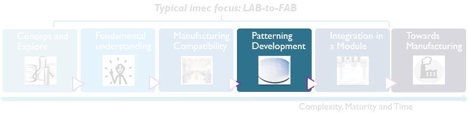
3 EUV ACTIVITIES AT IMEC: LAB-TO-FAB Typical imec focus: LAB-to-FAB Concept and Explore Fundamental understanding Manufacturi ng Compatibilit y Patterning Developmen t Integration in a Module Towards Manufacturi ng Complexity, Maturity and Time TODAY s FOCUS 3
4 OUTLINE IMEC TECH. NODEs MATERIAL LANDSCAPE IN EUVL EUV RESIST PATTERNING Line-space (LS) Contact holes (CH) Pillars (PL) EUV SUBSTRATE FOR EUV RESIST 4
5 IMEC TECH. NODES
6 IMEC TECH.NODEs - PATTERNING ASSUMPTIONS DIMENSIONS INVOLVED 6

7 PATTERNING

8 in7 BEOL CURRENT LITHOGRAPHIC PERFORMANCE 8

9 in7 BEOL WHAT ARE THE CHALLENGES TODAY? DtS and LWR/LCDU reduction at same performance with no added defects 9
10 MATERIAL LANDSCAPE IN EUVL
11 EUV MATERIAL LANDSCAPE TODAY SOG CAR Tone reversal material Organic UL Metal Nano Particles Molecular resist TMAH dev. SOC RESISTS Ancillary materials Metal oxide Metal sensitizer CAR Solventbased dev. CVD layer Metal Hard Mask Sensitizer UL CAR = Chemically Amplified Resist MCR = Metal containing Resist PTD = Positive Tone Developer NTD = Negative Tone Developer SOC = Spin On Carbon SOG = Spin On Glass UL = underlayer Traditional materials Not traditional materials 11
12 EUV PATTERNING

13 LOW EXPOSURE DOSE EUV RESIST SCREENING BEST SAMPLE PER SUPPLIER 16nm dense lines space PITCH 32nm 13


14 BUT, MORE IMPORTANT ARE THE NANO FAILURES 16NM LS PITCH 32NM ken line CAR = Chemically Amplified Resist MOR = Metal Oxide Resist nano-bridge CAR MOR nano-bridge >To get rid of nano failures is more urgent than reduce LWR < 14

15 LOW EXPOSURE DOSE EUV RESIST SCREENING BEST SAMPLE PER SUPPLIER Dense regular contact holes - Pitch 36nm 15

16 BUT, (AGAIN) NANO FAILURES ARE MORE IMPORTANT DENSE REGULAR CONTACT HOLES PITCH 36NM CHs with tendency to merge CH with tendency to close >To get rid of nano failures is more urgent than reduce LCDU < 16
 Dark field is the preferred mask tonality because of defectivity, flare")
17 AVAILABLE EUV RESISTS VS APPLICATION OPPORTUNITIES tate-of-the-art today for dense features Pitch 38-36nm Dark field mask Positive Tone Process CONTACTS PTD-CAR PTD-CAR with sensitizer Novel PTD NCAR Negative Tone Process PILLARS Metal Oxide resist Bright field mask TONE REVERSAL PROCESS FROM PTD-CAR (as promising approach) Dark field is the preferred mask tonality because of defectivity, flare NTD-CAR & NCAR metal and non metal containing (molecular resist, Nano Particles, etc..) are not ready for P38/P36 yet 17

18 METAL OXIDE RESIST REGULAR DENSE PILLARS PITCH 38NM CD 20.5nm 30 mj/cm 2 Low exposure dose resist 18
 FROM CONTACTS")


19 TONE REVERSAL PROCESS (TRP) FROM CONTACTS PILLARS TRP can be an alternative scheme to single exposure to make pillars from contacts 19
20 SUBSTRATES FOR EUV RESISTS

21 SUBSTRATES CAN BE TUNABLE FOR EUV RESIST SENSITIVITY IMPROVEMENT, PENALTY IS ON THE LWR 21

22 SUBSTRATES CAN BE TUNABLE FOR EUV RESIST SENSITIVITY IMPROVEMENT, LCDU STILL OK A ~ 22

23 EUV SUBSTRATES VS PHOTOEMISSION PROPERTY OF THE SUBSTRATE B photoemission DoF seems to correlate with photoemission of substrates Dose doesn t correlate Substrate design can play a role in the resist design development 23

24 FROM THE LAB TO THE FAB INPRIA CASE

25 METAL *1E10 (AT/CM2) METAL CROSS CONTAMINATION TEST - MOx RESIST OPTIMIZED PATH FOR A NON X-CONTAMINATING PROCESS contamination SPEC metal < : 1E10 at/cm 2 0,05 0,04 0,03 0,024 0,022 0,019 0,02 0,01 0,008 0,002 0 Front-side Front-Side - SB Back-side Back-Side - SB detection limit PRE process after 200 wfs Contamination 1.5x order of magnitude less w.r.t. to the spec De Simone et al. ICPST

26 DRY ETCH ETCH RATE INVESTIGATION OF MOx Etch step type BARC opening UL opening SOG opening SOC opening e Etch chemistry Cl2/O2 CF4/O2/CH2F2 Cl2/O2/N2 SF6/N2/CH2F2/H The etch selectivity of MCR vs SOC is 1:40. Simplified litho-etch process scheme can be designed to integrate MOx resist on advanced process modules of new technology devices De Simone et al. ICPST


27 ETCHER CONTAMINATION MARATHON OF MOx RESIST Pre etch ICP-MS Etch Rates Particles SnOx wafer etch WDC 24wafers/cycle Post etch ICP-MS Etch Rates Particles TEM metal-oxide removal Spec < 1E10 at/cm 2 95 processed wafers Wafer front side and backside metal contamination trended below spec level < 1E10 at/cm2 Etch rates are stable thermal oxide and i-line Resist De Simone et al. SPIE
 successful")
 SEM inspection and review Pattern litho sensitivity on MOx resist")

28 DETECTABILITY OF PROGRAMMED DEFECTS AFTER LITHO 22nm dense LS patterning MOx resist successful defect counting rate % Programmed defect size (nm) successful defect capturing rate % Programmed defect size (nm) Critical Point Inspection (SEM inspection) SEM inspection and review Pattern litho sensitivity on MOx resist shows some limitations on the inspection tool to detect the target programmed defects and defectivity inspection after etch is necessary at this stage De Simone et al. SPIE


29 Pitch 175nm Pitch 60nm Pitch 42nm MOx RESIST: ETCH DEVELOPMENT FOR in7 BLOCK LAYER SPIN-ON-CARBON OPENING after development Spin-On-Carbon opening CD: 25.5 nm Height : 12nm CD: 22.2 nm Height : 69.8nm High Resist-SOC etch selectivity CD: 25.6 nm Height : 11nm CD: 22.7 nm Height: 67.1nm Straight SOC pillar profile CD: 25.5 nm Height : 12nm De Simone et al. SPIE CD: 23.2 nm Height : 66.5nm Constant litho-etch CD bias through pitch for these structures


30 INTEGRATION FOR EUV in7 BLOCK LAYER Bright mask Dark mask EUV block mask Dark Tone Mask combined with Negative Tone Resist NT resist ArFi Core SAQP direct PT resist tone reversal Higher CoO Dark field is the preferred mask tonality because of defectivity, flare De Simone et al. SPIE


31 32P METAL (FOUNDRY N5) OPTION: SAQP + MOx RESIST EUV BLOCK P32 spacers on TiN Block litho on SOC SOC etch TiN etch Low-k etch Industry first assessment of SAQP + EUV single expose block with metal oxide (inpria) resist Integration into BEOL electrical test vehicle Joost Bekaert, SPIE 2017 SAQP = self-aligned quadrupole patterning 31
 Waikin Li, EUVL Symposium 2017 32")
32 EXTENSION TO in5 (FOUNDRY N3) Development of options for ~20-24 nm pitch metal blocks using metal oxide resist i.e.: Litho-develop-litho-etch process (LDLE) Waikin Li, EUVL Symposium
33 SUMMARY
34 SUMMARY Pitch 32nm LS and Pitch 36nm CH (in7 tech node): Low exposure dose is achieved but is limited by stochastics. Nano failures (bridges, broken lines, merging, close CHs) are becoming the 1 st priority to fix on top of LWR/LCDU reduction A new metric is needed to quantify the nano failures at early R&D phase LWR will require post processing smoothing approaches (litho & etch) More Negative Tone Systems (NTI or NTD) with high resolution are needed for pillar patterning. Tone Reversal Process from PTD-CAR can be an alternative approach for single pillar exposure Substrate plays a role in the EUV resist performance A dedicated substrate design could improve the resist sensitivity without a significant impact on LCDU The Lab-to-Fab path for advance patterning is in place at imec and through that, novel materials (as metal-oxide resists) can be enabled to reach the HVM grade for EUV lithography 34


35 ACKNOWLEDGEMENTS


36 Thank you for your attention 36
Metal Oxide EUV Photoresists for N7 Relevant Patterns
 Metal Oxide EUV Photoresists for N7 Relevant Patterns Stephen T. Meyers, Andrew Grenville 2016 International Workshop on EUV Lithography Resists Designed for EUV Lithography Integration Stochastic Variability
Lithography options for the 32nm half pitch node. imec
 Lithography options for the 32nm half pitch node imec 2006 1 Lithography options for the 32nm half pitch node Luc Van den hove and Kurt Ronse ITRS roadmap:32 nm half pitch requirement Product Half-Pitch,
Next Generation Source Power Requirements. Erik R. Hosler
 Next Generation Source Power Requirements Erik R. Hosler What will we need at the 3 nm node and beyond? Can laser produced plasma sources continue the roadmap? Needs to future EUV manufacturing Lithography
Technical Data Sheet Technisches Datenblatt
 AZ ECI 3000 Photoresist Universal i-line/crossover Photoresist Series GENERAL INFORMATION AZ ECI 3000 photoresist series are a family of fast positive resists with high resolution capabilities (0.4 µm
Advanced Lithography Updates and Challenges for Metrology and Inspection
 Advanced Lithography Updates and Challenges for Metrology and Inspection Center for Semiconductor Research & Development Advanced Lithography Process Technology Dept. Tatsuhiko Higashiki Contents Device
NIL defect performance toward High volume mass production
 NIL defect performance toward High volume mass production Masayuki Hatano a, Kei Kobayashi a, Hiroyuki Kashiwagi a, Hiroshi Tokue a, Takuya Kono a, Nakasugi Tetsuro a, Eun Hyuk Choi b, Wooyung Jung b a
Surface Preparation and Cleaning Conference April 19-20, 2016, Santa Clara, CA, USA. Nano-Bio Electronic Materials and Processing Lab.
 Surface Preparation and Cleaning Conference April 19-20, 2016, Santa Clara, CA, USA Issues on contaminants on EUV mask Particle removal on EUV mask surface Carbon contamination removal on EUV mask surface
AZ P4620 Photoresist Data Package
 AZ P4620 Photoresist Data Package The information contained herein is, as far as we are aware, true and accurate. However, no representations or warranties, either express or implied, whether of merchantable
New Materials as an enabler for Advanced Chip Manufacturing
 New Materials as an enabler for Advanced Chip Manufacturing Drive Innovation, Deliver Excellence ASM International Analyst and Investor Technology Seminar Semicon West July 10 2013 Outline New Materials:
Photolithography I ( Part 2 )
") 1 Photolithography I ( Part 2 ) Chapter 13 : Semiconductor Manufacturing Technology by M. Quirk & J. Serda Bjørn-Ove Fimland, Department of Electronics and Telecommunication, Norwegian University of Science
1 Photolithography I ( Part 2 ) Chapter 13 : Semiconductor Manufacturing Technology by M. Quirk & J. Serda Bjørn-Ove Fimland, Department of Electronics and Telecommunication, Norwegian University of Science
FIB mask repair technology for EUV mask 1. INTRODUCTION
 FIB mask repair technology for EUV mask Tsuyoshi Amano*, Yasushi Nishiyama*, iroyuki Shigemura*, Tsuneo Terasawa*, Osamu Suga*, Kensuke Shiina**, Fumio Aramaki**, Anto Yasaka** Tsukasa Abe***, iroshi Mohri***
TSV Processing and Wafer Stacking. Kathy Cook and Maggie Zoberbier, 3D Business Development
 TSV Processing and Wafer Stacking Kathy Cook and Maggie Zoberbier, 3D Business Development Outline Why 3D Integration? TSV Process Variations Lithography Process Results Stacking Technology Wafer Bonding
Enabling Low Defectivity Solutions Through Co- Development of CMP Slurries and Cleaning Solutions for Cobalt Interconnect Applications
 Enabling Low Defectivity Solutions Through Co- Development of CMP Slurries and Cleaning Solutions for Cobalt Interconnect Applications Dnyanesh Tamboli 1, Tom Shi 1, Chris Li 2, Ming-Shih Tsai 2, Rung-Je
Photoresist Coat, Expose and Develop Laboratory Dr. Lynn Fuller
 ROCHESTER INSTITUTE OF TECHNOLOGY MICROELECTRONIC ENGINEERING Photoresist Coat, Expose and Develop Laboratory Dr. Lynn Fuller Webpage: http://www.rit.edu/lffeee 82 Lomb Memorial Drive Rochester, NY 14623-5604
Simulation Analysis of Defect Repair Methods for EUVL Mask Blanks
 Simulation Analysis of Defect Repair Methods for EUVL Mask Blanks Association of Super-Advanced Electronics Technologies (ASET) EUV Process Technology Research Laboratory Takeo Hashimoto and Iao Nishiyama
EUV Defect Repair Strategy
 EUV Defect Repair Strategy J.H. Peters, S. Perlitz, U. Matejka, W. Harnisch, D. Hellweg, M. Weiss, M. Waiblinger, T. Bret, T. Hofmann, K. Edinger, K. Kornilov Carl Zeiss SMS / SMT 2011 International Symposium
TSV Interposer Process Flow with IME 300mm Facilities
 TSV Interposer Process Flow with IME 300mm Facilities Property of Institute of Microelectronics (IME)-Singapore August 17, 2012 Outline 1. TSV interposer (TSI) cross sectional schematic TSI with BEOL,
Status and Challenges in EUV Mask Cleaning
 MA-P03 Status and Challenges in EUV Mask Cleaning Ted Liang, Grace Ng, Guojing Zhang, Henry Yun, Ravi Jaiswal*, Intel Corporation * Summer Intern from Purdue University Takeya Shimomura, Toshiaki Motonaga
EUV Mask Image Placement Management in Writing, Registration, and Exposure Tools
 EUV Mask Image Placement Management in Writing, Registration, and Exposure Tools Eric Cotte a *, Uwe Dersch a, Christian Holfeld a, Uwe Mickan b, Holger Seitz c, Thomas Leutbecher c, and Günter Hess c
Post CMP Cleaning SPCC2017 March 27, 2017 Jin-Goo Park
 Post CMP Cleaning Conference @ SPCC2017 March 27, 2017 Jin-Goo Park Challenges in surface preparation Research trend in cleaning technology Lesson learned from current cleaning technology Challenges in
Integrated Process Technology Development for the sub 7nm Era
 Integrated Process Technology Development for the sub 7nm Era July 12, 2017 Alex Oscilowski President TEL Technology Center, America, LLC. TEL s Global R&D Operations Korea U.S. imec (Belgium) TEL Technology
Imprint Lithography: Getting to the Next Level
 Imprint Lithography: Getting to the Next Level May 26 SEMECH Litho Forum James E. Ellenson; ; Ken Kramer; im S. Hostetler; Laura King; William M. ong Hewlett-Packard Company 24 Hewlett-Packard Development
Resist Characterization for EUV- Lithography
 Resist Characterization for EUV- Lithography 2. Int. EUVL-Symposium, Antwerp, B Wolf-Dieter Domke 1, Stefan Hirscher 2, liver Kirch 3, Karl Kragler 1, Klaus Lowack 1, 1 Infineon Technologies AG, 91050
Advanced developer-soluble gap-fill materials and applications
 Advanced developer-soluble gap-fill materials and applications Runhui Huang, Dan Sullivan, Anwei Qin, Shannon Brown Brewer Science, Inc., 2401 Brewer Dr., Rolla, MO, USA, 65401 ABSTRACT For the via-first
UV5 POSITIVE DUV PHOTORESIST For Microlithography Applications
 UV5 POSITIVE DUV PHOTORESIST For Microlithography Applications DESCRIPTION UV5 positive DUV photoresist has been optimized to provide vertical profile imaging of isolated and semidense features for device
Nonplanar Metallization. Planar Metallization. Professor N Cheung, U.C. Berkeley
 Nonplanar Metallization Planar Metallization Passivation Metal 5 (copper) Metal 3 (copper) Interlevel dielectric (ILD) Via (tungsten) Metal 1 (copper) Tungsten Plug to Si Silicon Caps and Plugs oxide oxide
Chapter 1.6. Polished Single-Crystal Silicon, Prime Wafers (all numbers nominal) Wafer Specification Table. Diameter 100 mm 4-inch 150 mm 6-inch
 Wafer Specification Table. Diameter 100 mm 4-inch 150 mm 6-inch") Chapter 1.6 I - Substrate Specifications Polished Single-Crystal Silicon, Prime Wafers (all numbers nominal) Wafer Specification Table Diameter 100 mm 4-inch 150 mm 6-inch Thickness 525 µm 20.5 mils 675
Chapter 1.6 I - Substrate Specifications Polished Single-Crystal Silicon, Prime Wafers (all numbers nominal) Wafer Specification Table Diameter 100 mm 4-inch 150 mm 6-inch Thickness 525 µm 20.5 mils 675
Ultra Fine Pitch Bumping Using e-ni/au and Sn Lift-Off Processes
 Ultra Fine Pitch Bumping Using e-ni/au and Sn Lift-Off Processes Andrew Strandjord, Thorsten Teutsch, and Jing Li Pac Tech USA Packaging Technologies, Inc. Santa Clara, CA USA 95050 Thomas Oppert, and
Multilayer Development for Extreme Ultraviolet and Shorter Wavelength Lithography
 Multilayer Development for Extreme Ultraviolet and Shorter Wavelength Lithography Eric Louis 1, Igor Makhotkin 1, Erwin Zoethout 1, Stephan Müllender 2 and Fred Bijkerk 1,3 1 FOM Institute for Plasma Physics
125nXT Series. EMD PeRFoRmaNce MaTeRIaLs. technical datasheet. Photopolymer Negative Tone Photoresists APPLICATION TYPICAL PROCESS THICKNESS GRADES
 EMD PeRFoRmaNce MaTeRIaLs technical datasheet AZ 125nXT Series Photopolymer Negative Tone Photoresists APPLICATION Thick photopolymer photoresists featuring aspect ratios and photospeed not possible with
Process Flow in Cross Sections
 Process Flow in Cross Sections Process (simplified) 0. Clean wafer in nasty acids (HF, HNO 3, H 2 SO 4,...) --> wear gloves! 1. Grow 500 nm of SiO 2 (by putting the wafer in a furnace with O 2 2. Coat
Electron Beam Induced Processes and their Applicability to Mask Repair
 & Electron Beam Induced Processes and their Applicability to Mask Repair Hans W.P. Koops (1), Volker Boegli (1), Klaus Edinger (1), Johannes Bihr (2), Jens Greiser (2), (1) NaWoTec GmbH Rossdorf Germany
Advantages of BARC and photoresist matching for 193-nm photosensitive BARC applications
 Advantages of BARC and photoresist matching for 193-nm photosensitive BARC applications Joyce Lowes a, Victor Pham b, Jim Meador a, Charlyn Stroud a, Ferdinand Rosas b, Ramil-Marcelo L. Mercado a, Mark
Seminar Micro- and Nano-technology
 Seminar Micro- and Nano-technology Seminar 1 Schedule Wednesday 17:45-18:30 Yannick Bourgin yannick.bourgin@uni-jena.de Phone: +49(3641)947990 www.iap.uni-jena.de Presentations 2 Presentation by 2 students
DuPont MX5000 Series
 DuPont MX5000 Series DATA SHEET & PROCESSING INFORMATION High Performance Multi-Purpose Polymer Film for MEMS Applications PRODUCT FEATURES/ APPLICATIONS Negative working, aqueous processable dry film
Overview of SEMI Standards for EUV Masks. Scott Hector ISMT/Motorola Chairman of SEMI EUV Mask Task Force
 Overview of SEMI Standards for EUV Masks Scott Hector ISMT/Motorola Chairman of SEMI EUV Mask Task Force 1 4 Storage container and attributes of removable protection mechanism (3553) Removable protection
Amorphous Oxide Transistor Electrokinetic Reflective Display on Flexible Glass
 Amorphous Oxide Transistor Electrokinetic Reflective Display on Flexible Glass Devin A. Mourey, Randy L. Hoffman, Sean M. Garner *, Arliena Holm, Brad Benson, Gregg Combs, James E. Abbott, Xinghua Li*,
2006 UPDATE METROLOGY
 INTERNATIONAL TECHNOLOGY ROADMAP FOR SEMICONDUCTORS METROLOGY THE ITRS DEVED AND INTENDED FOR TECHNOLOGY ASSESSMENT ONLY AND WITHOUT REGARD TO ANY COMMERCIAL CONSIDERATIONS PERTAINING TO INDIVIDUAL PRODUCTS
Lithography Tool Package
 4. Development Thomas Anhøj and Tine Greibe Outline 1. Introduction Process steps in UV lithography 2. Spin coating Resist composition Pre-treatment Principle Softbake Spin curve 3. Exposure Hardware Process
EUVL Mask Defect Strategy
 EUVL Mask Defect Strategy EUV Mask March 4, 2002, Santa Clara, CA Alan Stivers, Ted Liang, Barry Lieberman, Pei-yang Yan, Fu-Chang Lo Intel Corporation, Santa Clara, CA USA Outline Introduction Overall
Novel Spin on Planarization Technology by Photo Curing SOC (P-SOC)
") Journal of Photopolymer Science and Technology Volume 3, Number 3 (17) 373-378 C 17SPST Technical Paper Novel Spin on Planarization Technology by Photo Curing (P-) Takafumi Endo*, Rikimaru Sakamoto, Keisuke
Journal of Photopolymer Science and Technology Volume 3, Number 3 (17) 373-378 C 17SPST Technical Paper Novel Spin on Planarization Technology by Photo Curing (P-) Takafumi Endo*, Rikimaru Sakamoto, Keisuke
Defects, Overlay and Focus Performance Improvements with Five Generations of Immersion Exposure Systems
 Defects, Overlay and Focus Performance Improvements with Five Generations of Immersion Exposure Systems Jan Mulkens, Bob Streefkerk, Hans Jasper, Jos de Klerk, Fred de Jong, Leon Levasier and Martijn Leenders.
ZERO DEFECTS Entegris Newsletter
 July 215 CONTENTS 1. Entegris News Entegris Reaches Milestones at its i2m Center for Advanced Materials Science Entegris @ SEMICON West 2. Process Stability InVue CR288 Concentration Monitor Application
Blisters formation mechanism during High Dose Implanted Resist Stripping
 Blisters formation mechanism during High Dose Implanted Resist Stripping Marion Croisy a,b,c*, Cécile Jenny a, Claire Richard a, Denis Guiheux a, Sylvain Joblot a, Alain Campo b, Erwine Pargon c, Nicolas
Laser Produced Plasma for Production EUV Lithography
 TRW / Cutting Edge Optronics Laser Produced Plasma for Production EUV Lithography EUVL Source Workshop October 29, 2001 TRW/CEO Laser-Produced Plasma (LPP) EUV Source Development and Commercialization
Hybrid BARC approaches for FEOL and BEOL integration
 Hybrid BARC approaches for FEOL and BEOL integration Willie Perez a, Stephen Turner a, Nick Brakensiek a, Lynne Mills b, Larry Wilson b, Paul Popa b a Brewer Science, Inc., 241 Brewer Dr., Rolla, MO 6541
Customer Support: Leveraging Value of Ownership
 Customer Support: Leveraging Value of Ownership Bernard Carayon SVP Customer Support WW Analyst Day, 30 September 2004 / Slide 1 Agenda! Customer Support main activities! Worldwide Organization and installed
THE IMPACT OF 3D DEVICES ON THE FUTURE OF PROCESS MATERIALS TRENDS & OPPORTUNITIES
 THE IMPACT OF 3D DEVICES ON THE FUTURE OF PROCESS MATERIALS TRENDS & OPPORTUNITIES L. Shon Roy K. Holland, PhD. October 2014 Materials Examples Process materials used to make semiconductor devices Gases
A World Class Specialty Materials Company
 SEMICON KOREA MEDIA BRIEFING A World Class Specialty Materials Company Richard Hong President, Entegris Korea AGENDA 01 A World Class Specialty Materials Company 02 Entegris in Korea 03 Q&A 04 Meeting
Nanoimprinting in Polymers and Applications in Cell Studies. Albert F. YEE Chemical Engineering & Materials Science UC Irvine
 Nanoimprinting in Polymers and Applications in Cell Studies Albert F. YEE Chemical Engineering & Materials Science UC Irvine Presentation outline Motivation Reversal imprinting Soft inkpad imprinting on
Novel Polyphenol Base Molecular Resist Having High Thermal Resistance
 Novel olyphenol Base Molecular Resist Having High Thermal Resistance Taku Hirayama, Takeyoshi Mimura, Jun Iwashita, Makiko Irie, Daiju hiono, Hideo Hada and Takeshi Iwai TKY KA KGY C., LTD. 2008 International
VLSI Systems and Computer Architecture Lab
 ΚΥΚΛΩΜΑΤΑ VLSI Πανεπιστήμιο Ιωαννίνων CMOS Technology Τμήμα Μηχανικών Η/Υ και Πληροφορικής 1 From the book: An Introduction ti to VLSI Process By: W. Maly ΚΥΚΛΩΜΑΤΑ VLSI Διάρθρωση 1. N well CMOS 2. Active
If it moves, chop it in half, then simulate it
 Interactions of Double Patterning Technology with wafer processing, OPC and design flows Kevin Lucas, Chris Cork, Alex Miloslavsky, Gerry Luk-Pat, Levi Barnes, John Hapli, John Lewellen, Greg Rollins Synopsys
3.155J / 6.152J Micro/Nano Processing Technology TAKE-HOME QUIZ FALL TERM 2005
 3.155J / 6.152J Micro/Nano Processing Technology TAKE-HOME QUIZ FALL TERM 2005 1) This is an open book, take-home quiz. You are not to consult with other class members or anyone else. You may discuss the
SUSS SOLUTIONS FOR LARGE FORMAT PATTERNING UV Scanning Lithography and Excimer Laser Ablation
 SUSS SOLUTIONS FOR LARGE FORMAT PATTERNING UV Scanning Lithography and Excimer Laser Ablation Kevin Yang, Habib Hichri, Ralph Zoberbier SÜSS MicroTec Photonic Systems Inc. June 18, 2015 MARKET DRIVER Mobile
Emerging Materials for Front End IC Process
 Emerging Materials for Front End IC Process Mark Thirsk Linx Consulting +1 617 273 8837 mthirsk@linx-consulting.com Device Making Unit Operations - 2007 100% 0.065 Total = 12,229,682 80 0.09 60 40 0.13
3D & 2½D Test Challenges Getting to Known Good Die & Known Good Stack
 1 3D & 2½D Test Challenges Getting to Known Good Die & Known Good Stack Advantest Corporation 2 The final yield Any Multi-die Product Must Consider the Accumulated Yield Assume Test Can Provide 99% Die
Metallization deposition and etching. Material mainly taken from Campbell, UCCS
 Metallization deposition and etching Material mainly taken from Campbell, UCCS Application Metallization is back-end processing Metals used are aluminum and copper Mainly involves deposition and etching,
How To Write A Flowchart
 1 Learning Objectives To learn how you transfer a device concept into a process flow to fabricate the device in the EKL labs You learn the different components that makes up a flowchart; process blocks,
Contact Resistance Reduction using Advanced Implant and Anneal Techniques for 7nm Node and Beyond
 Contact Resistance Reduction using Advanced Implant and Anneal Techniques for 7nm Node and Beyond Fareen Adeni Khaja Global Product Manager, Front End Products Transistor and Interconnect Group NCCAVS
Galvanic Porous Silicon for High Velocity Nanoenergetics
 Supporting Information Galvanic Porous Silicon for High Velocity Nanoenergetics Collin R. Becker 1,2, Steven Apperson 3, Christopher J. Morris 2, Shubhra Gangopadhyay 3, Luke J. Currano 2, Wayne A. Churaman
Rockwell R RF to IF Down Converter
 Construction Analysis Rockwell R6732-13 RF to IF Down Converter Report Number: SCA 9709-552 Global Semiconductor Industry the Serving Since 1964 17350 N. Hartford Drive Scottsdale, AZ 85255 Phone: 602-515-9780
Electron Beam Lithography - key enabling technology in nanofabrication. Frank Dirne
 Electron Beam Lithography - key enabling technology in nanofabrication Frank Dirne Moore s Law (x2/2 yr) Moore s Law EBL Electron Beam Lithography - key enabling technology in nanofabrication - Principles
Micro and nano structuring of carbon based materials for micro injection moulding and hot embossing
 Micro and nano structuring of carbon based materials for micro injection moulding and hot embossing Victor Usov, Graham Cross, Neal O Hara, Declan Scanlan, Sander Paulen, Chris de Ruijter, Daniel Vlasveld,
2015 EE410-LOCOS 0.5µm Poly CMOS Process Run Card Lot ID:
 STEP 0.00 - PHOTOMASK #0- ZERO LEVEL MARKS Starting materials is n-type silicon (5-10 ohm-cm). Add four test wafers labeled T1-T4. T1 and T2 will travel with the device wafers and get all of the processing
Application of ultra-thin aluminum oxide etch mask made by atomic layer deposition technique
 IOP Publishing Journal of Physics: Conference Series 61 (2007) 369 373 doi:10.1088/1742-6596/61/1/074 International Conference on Nanoscience and Technology (ICN&T 2006) Application of ultra-thin aluminum
EE40 Lec 22. IC Fabrication Technology. Prof. Nathan Cheung 11/19/2009
 Suggested Reading EE40 Lec 22 IC Fabrication Technology Prof. Nathan Cheung 11/19/2009 300mm Fab Tour http://www-03.ibm.com/technology/manufacturing/technology_tour_300mm_foundry.html Overview of IC Technology
Deep Silicon Etching An Enabling Technology for Wireless Systems Segment By Carson Ogilvie and Joel Goodrich Commercial Product Solutions
 Deep Silicon Etching An Enabling Technology for Wireless Systems Segment By Carson Ogilvie and Joel Goodrich Commercial Product Solutions Abstract The recent installation of a new etch tool, the Surface
EXCIMER LASER ANNEALING FOR LOW- TEMPERATURE POLYSILICON THIN FILM TRANSISTOR FABRICATION ON PLASTIC SUBSTRATES
 EXCIMER LASER ANNEALING FOR LOW- TEMPERATURE POLYSILICON THIN FILM TRANSISTOR FABRICATION ON PLASTIC SUBSTRATES G. Fortunato, A. Pecora, L. Maiolo, M. Cuscunà, D. Simeone, A. Minotti, and L. Mariucci CNR-IMM,
Manufacturer Part Number. Module 2: CMOS FEOL Analysis
 Manufacturer Part Number description Module 2: CMOS FEOL Analysis Manufacturer Device # 2 Some of the information is this report may be covered by patents, mask and/or copyright protection. This report
Reactor wall plasma cleaning processes after InP etching in Cl 2 /CH 4 /Ar ICP discharge
 Reactor wall plasma cleaning processes after InP etching in Cl 2 /CH 4 /Ar ICP discharge R. Chanson a, E. Pargon a, M. Darnon a, C. Petit Etienne a, S. David a, M. Fouchier a, B. Glueck b, P. Brianceau
Semicon Europa Wafer Chucks for Lithography. Berliner Glas KGaA Herbert Kubatz GmbH & Co. Sven Götze
 Semicon Europa 2011. Wafer Chucks for Lithography. Berliner Glas KGaA Herbert Kubatz GmbH & Co. Sven Götze 1 Export driven, medium-sized, innovative. Solutions in Optics High Tech in Glass Legal form:
Nanofabrication Prof. Stephen Y. Chou NanoStructure Laboratory
 Nanofabrication Prof. Stephen Y. Chou Department of Electrical Engineering Princeton University 1 Acknowledgment Dr. Paul Fischer Dr. Yun Wang Dr. Jay Guo Dr. Peter Klauss Dr. Jim Wang Dr. Longtin He Dr.
Atomic Layer Deposition(ALD)
") Atomic Layer Deposition(ALD) AlO x for diffusion barriers OLED displays http://en.wikipedia.org/wiki/atomic_layer_deposition#/media/file:ald_schematics.jpg Lam s market-leading ALTUS systems combine CVD
Atomic Layer Deposition(ALD) AlO x for diffusion barriers OLED displays http://en.wikipedia.org/wiki/atomic_layer_deposition#/media/file:ald_schematics.jpg Lam s market-leading ALTUS systems combine CVD
Introduction to Micro/Nano Fabrication Techniques. Date: 2015/05/22 Dr. Yi-Chung Tung. Fabrication of Nanomaterials
 Introduction to Micro/Nano Fabrication Techniques Date: 2015/05/22 Dr. Yi-Chung Tung Fabrication of Nanomaterials Top-Down Approach Begin with bulk materials that are reduced into nanoscale materials Ex:
Filtration on block copolymer solution used in directed self assembly lithography
 Filtration on block copolymer solution used in directed self assembly lithography Toru Umeda*, Tomoyuki Takakura and Shuichi Tsuzuki Nihon Pall Ltd., 46 Kasuminosato, Ami-machi, Inashiki-gun, Ibaraki,
FOR SEMICONDUCTORS 2005 EDITION
 INTERNATIONAL TECHNOLOGY ROADMAP FOR SEMICONDUCTORS 2005 EDITION YIELD ENHANCEMENT THE ITRS IS DEVISED AND INTENDED FOR TECHNOLOGY ASSESSMENT ONLY AND IS WITHOUT REGARD TO ANY COMMERCIAL CONSIDERATIONS
Nano-imprinting Lithography Technology І
 Nano-imprinting Lithography Technology І Agenda Limitation of photolithograph - Remind of photolithography technology - What is diffraction - Diffraction limit Concept of nano-imprinting lithography Basic
Panel Discussion: Advanced Packaging
 Dr. Steve Bezuk Senior Director IC Packaging Engineering Qualcomm Technologies, Inc. Panel Discussion: Advanced Packaging PAGE 1 Technical Challenges of Packaging (Mobile Focus) Materials Die materials
A novel approach to developer-soluble anti-reflective coatings for 248-nm lithography
 A novel approach to developer-soluble anti-reflective coatings for 248-nm lithography Ramil-Marcelo L. Mercado, Joyce A. Lowes, Carlton A. Washburn, Douglas J. Guerrero Brewer Science, Inc., 2401 Brewer
CMP Users Meeting. Impact of CMP buffing chemistry on defects level for interconnections on CMOS processing. April 12 th 2013 D.
 Impact of CMP buffing chemistry on defects level for interconnections on CMOS processing CMP Users Meeting April 12 th 2013 D.JEANJEAN Damien JEANJEAN Olivier ROBIN Sebastien GAILLARD David GALPIN Grégoire
Intel Pentium Processor W/MMX
 Construction Analysis Intel Pentium Processor W/MMX Report Number: SCA 9706-540 Global Semiconductor Industry the Serving Since 1964 15022 N. 75th Street Scottsdale, AZ 85260-2476 Phone: 602-998-9780 Fax:
Packaging Commercial CMOS Chips for Lab on a Chip Integration
 Supporting Information for Packaging Commercial CMOS Chips for Lab on a Chip Integration by Timir Datta-Chaudhuri, Pamela Abshire, and Elisabeth Smela Biocompatibility Although the supplier s instructions
Creating Greater Capacity on Smaller Spaces
 Creating Greater Capacity on Smaller Spaces Manufacturability of Pattern Media Babak Heidari, Obducat, Sweden Obducat Overview Company Background Founded in 1989 Facilities in Sweden (HQ) and in Cambridge
Sub-5 nm Structures Process Development and Fabrication Over Large Areas
 A S Jugessur,, 2017, 1:1 SciFed Nanotech Research Letters Research Article Open Access Sub-5 nm Structures Process Development and Fabrication Over Large Areas * A S Jugessur * University of Iowa Microfabrication
Dr. Priyabrat Dash Office: BM-406, Mob: Webpage: MB: 205
 Email: dashp@nitrkl.ac.in Office: BM-406, Mob: 8895121141 Webpage: http://homepage.usask.ca/~prd822/ MB: 205 Nonmanufacturing In continuation from last class... 2 Top-Down methods Mechanical-energy methods
Simple method for formation of nanometer scale holes in membranes. E. O. Lawrence Berkeley National Laboratory, Berkeley, CA 94720
 Simple method for formation of nanometer scale holes in membranes T. Schenkel 1, E. A. Stach, V. Radmilovic, S.-J. Park, and A. Persaud E. O. Lawrence Berkeley National Laboratory, Berkeley, CA 94720 When
FOR SEMICONDUCTORS 2007 EDITION
 INTERNATIONAL TECHNOLOGY ROADMAP FOR SEMICONDUCTORS 2007 EDITION YIELD ENHANCEMENT THE ITRS IS DEVISED AND INTENDED FOR TECHNOLOGY ASSESSMENT ONLY AND IS WITHOUT REGARD TO ANY COMMERCIAL CONSIDERATIONS
IMPLEMENTATION OF A FULLY MOLDED FAN-OUT PACKAGING TECHNOLOGY
 IMPLEMENTATION OF A FULLY MOLDED FAN-OUT PACKAGING TECHNOLOGY B. Rogers, C. Scanlan, and T. Olson Deca Technologies, Inc. Tempe, AZ USA boyd.rogers@decatechnologies.com ABSTRACT Fan-Out Wafer-Level Packaging
State of the art quality of a GeOx interfacial passivation layer formed on Ge(001)
") APPLICATION NOTE State of the art quality of a Ox interfacial passivation layer formed on (001) Summary A number of research efforts have been made to realize Metal-Oxide-Semiconductor Field Effect Transistors
APPLICATION NOTE State of the art quality of a Ox interfacial passivation layer formed on (001) Summary A number of research efforts have been made to realize Metal-Oxide-Semiconductor Field Effect Transistors
ULTRA-SMALL VIA-TECHNOLOGY OF THINFILM POLYMERS USING ADVANCED SCANNING LASER ABLATION
 ULTRA-SMALL VIA-TECHNOLOGY OF THINFILM POLYMERS USING ADVANCED SCANNING LASER ABLATION Michael Töpper Fraunhofer Research Institution for Reliability and Microintegration IZM Germany Martin Wilke, Klaus-Dieter
Process Optimization in Post W CMP In-situ Cleaning. Hong Jin Kim, Si-Gyung Ahn, Liqiao Qin CMP, Advanced Module Engineering GLOBALFOUNDRIES, USA
 Process Optimization in Post W CMP In-situ Cleaning Hong Jin Kim, Si-Gyung Ahn, Liqiao Qin CMP, Advanced Module Engineering GLOBALFOUNDRIES, USA Contents W CMP process for sub 14nm device W Gate CMP W
Optimizing spray coater process parameters
 Optimizing spray coater process parameters Dr. Eleonora Storace, Florian Palitschka, Dr. Dietrich Tönnies SUSS MicroTec Lithography GmbH Germany Published in the SUSS report 01/2014 E-mail: info@suss.com
Part 3: Test Structures, Test Chips, In-Line Metrology & Inspection
 Part 3: Test Structures, Test Chips, In-Line Metrology & Inspection CTO, Maydan Technology Center Applied Materials, Inc. Mike_Smayling@amat.com Topics Introduction to Test Chips Test Structures Basic
Hybrid III-V/Si DFB laser integration on a 200 mm fully CMOS-compatible silicon photonics platform
 Hybrid III-V/Si DFB laser integration on a 200 mm fully CMOS-compatible silicon photonics platform B. Szelag 1, K. Hassan 1, L. Adelmini 1, E. Ghegin 1,2, Ph. Rodriguez 1, S. Bensalem 1, F. Nemouchi 1,
The image part with relationship ID rid4 was not found in the file. Welcome
 The image part with relationship ID rid4 was not found in the file. Welcome Trace Metals Analysis: Impurity Determinations By Thomas Kozikowski Chemist, R&D at Inorganic Ventures Key Considerations What
High Performance, Ceria Post-CMP Cleaning Formulations for STI/ILD Dielectric Substrates
 SPCC POST-CMP CONFERENCE High Performance, Ceria Post-CMP Cleaning Formulations for STI/ILD Dielectric Substrates Daniela White*, PhD Sr. Principal Scientist Atanu Das, PhD Scientist Thomas Parson, PhD
IISW-2009 BSI technical challenges
 IISW-2009 BSI technical challenges Bergen. 25th June 2009 Outline BSI consumer vs BSI scientific BSI vs FSI Remaining challenges Charges collection BSI overlay challenges BSI laser annealing Thinning Process
Cu Wiring Process for TFTs - Improved Hydrogen Plasma Resistance with a New Cu Alloy -
 Cu Wiring Process for TFTs - Improved Hydrogen Plasma Resistance with a New Cu Alloy - Masanori Shirai*, Satoru Takazawa*, Satoru Ishibashi*, Tadashi Masuda* As flat-screen TVs become larger and their
Silicon Wafer Processing PAKAGING AND TEST
 Silicon Wafer Processing PAKAGING AND TEST Parametrical test using test structures regularly distributed in the wafer Wafer die test marking defective dies dies separation die fixing (not marked as defective)