Manufacturer Part Number. Module 2: CMOS FEOL Analysis
|
|
|
- Benjamin Ellis
- 6 years ago
- Views:
Transcription
1 Manufacturer Part Number description Module 2: CMOS FEOL Analysis
2 Manufacturer Device # 2 Some of the information is this report may be covered by patents, mask and/or copyright protection. This report should not be taken as an inducement to infringe on these rights Chipworks Inc. This report is provided exclusively for the use of the purchasing organization. It can be freely copied and distributed within the purchasing organization, conditional upon the accompanying Chipworks accreditation remaining attached. Distribution of the entire report outside of the purchasing organization is strictly forbidden. The use of portions of the document for the support of the purchasing organization s corporate interest (e.g., licensing or marketing activities) is permitted, as defined by the fair use provisions of the copyright act. Accreditation to Chipworks must be attached to any yportion of the reproduced information. Report Code: IPR-XXXX-XXX.1 LOA# Revision XX Published: XX
3 Manufacturer Device # 3 Table of Contents (all CMOS Modules) Module 1: CMOS Overview Analysis Package photographs Package X-rays Determination of technology node based on SEM cross section Module 2: CMOS FEOL Analysis SEM and TEM analysis of isolation, MOS transistors and PMD Selected Materials analysis results Selected Materials analysis results Critical dimensions Module 3:CMOS BEOL Analysis SEM and TEM cross-sectional analysis of dielectrics, metals and vias. Materials analysis results for metals and dielectrics Critical dimensions Module 4:CMOS SRAM Analysis Plan-view analysis of minimum SRAM cell Cross-sectional SEM and TEM analysis of SRAM cell
4 Manufacturer Device # 4 Summary Slide Introduction Device Identification Process Summary Observed Critical Dimensions FEOL Analysis PMD TEM Contact Bottom and Silicide TEM NMOS and PMOS SEM Silicon Etch MOS Transistor TEM Contacted MOS Gates MOS Gate Detail MOS Gate Wrap MOS Gate Wrap Detail Gate Dielectric STI Depth Minimum Width STI Statement of Measurement Uncertainty and Scope Variation
5 Manufacturer Device # 5 Introduction The 45 nm XXXXXXXX was extracted from a XXXXXXX. [1] reference
6 Manufacturer Device # 6 Device Identification Manufacturer XXXXXXXXXX Foundry XXXXXXXXXX Part number XXXXXXXXXX Type XXXXXXXXXX Date code XXXXXXXXXX Package markings Package type XXXXXXXXXX XXXXXXXXXX XXXXXXXXXX BGA Package dimensions XX.X mm x XX.X mm x X.X mm thick Die markings XXXXXXXXXX Die size (die edge seal) 8.42 mm x 8.14 mm (65.5 mm2)
7 Manufacturer Device # 7 Process Summary Process type CMOS Number of metal layers 9 Minimum MOS transistor gate length 32 nm Process generation 45 nm Feature measured to determine process generation Contacted gate pitch and MOS gate length
8 Manufacturer Device # 8 Observed Critical Dimensions Width (µm) Space (µm) Pitch (µm) Thickness (µm) Metal Contacted Gates 0.18 Minimum MOS Gate Length 32 nm 0.11 Minimum STI
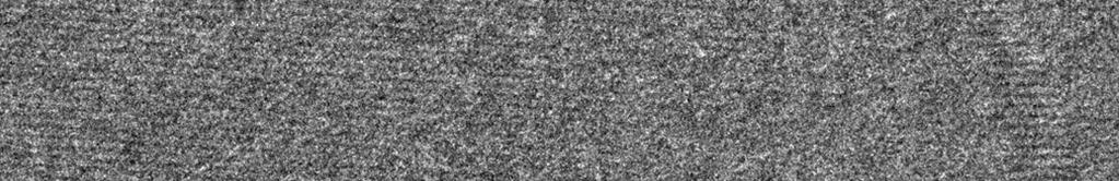
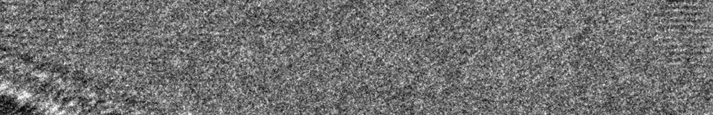
9 Manufacturer Device # 9 FEOL Analysis TEM and SEM cross-sectional analysis of metal 1, PMD, transistors and STI is included.


10 Manufacturer Device # 10 PMD TEM PMD 5 SiOC PMD 4 oxide M1 Cu PMD 3 oxide PMD 2 oxide 0.44 µm W contact PMD 1 - SiON poly gate NiSi NiSi


11 Manufacturer Device # 11 Contact Bottom and Silicide TEM W contact TiN liner ~5 nm ~12 nm NiSi ~8 nm Si substrate Contact bottom
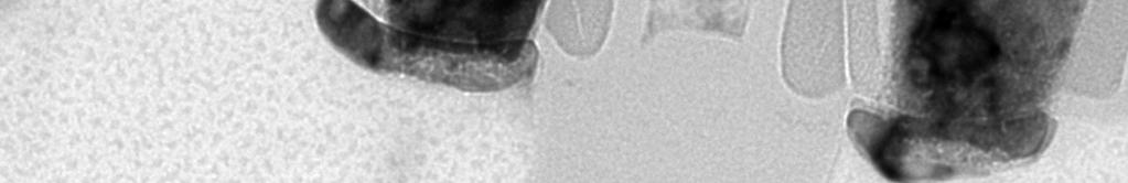
12 Manufacturer Device # 12 NMOS and PMOS SEM Silicon Etch NMOS PMOS


13 Manufacturer Device # 13 MOS Transistor TEM NiSi buffer oxide silicon nitride SWS polysilicon 32 nm NMOS and PMOS have the same physical structure


14 Manufacturer Device # 14 Contacted MOS Gates NiSi 30 nm 50 nm 190 nm 24 nm 40 nm 32 nm notch NiSi 29 nm 36 nm 33 nm
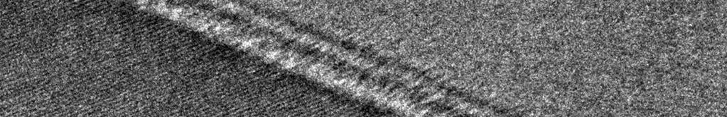
15 Manufacturer Device # 15 MOS Gate Detail NiSi buffer oxide 13 nm SiON CESL W contact 27 nm polysilicon ONO gate dielectric silicon nitride SWS 7 nm 22 nm 38 nm NiSi Si substrate


16 Manufacturer Device # 16 MOS Gate Wrap 16 nm NiSi 108 nm polysilicon 11 nm Si substrate STI


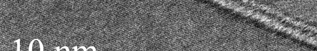
17 Manufacturer Device # 17 MOS Gate Wrap Detail polysilicon gate dielectric 13 nm Si substrate STI
18 Manufacturer Device # 18 Gate Dielectric polysilicon O N O 2.0 nm Si 2.0 nm ONO gate dielectric
19 Manufacturer Device # 19 STI Depth


20 Manufacturer Device # 20 Minimum Width STI W contact poly 0.11 µm 0.32 µm
21 Manufacturer Device # 21 Statement of Measurement Uncertainty and Scope Variation Measurement Uncertainty Chipworks calibrates length measurements on its scanning electron microscopes (SEM), transmission electron microscope (TEM), and optical microscopes, using measurement standards that are traceable to the International System of Units (SI). Our SEM/TEM cross-calibration calibration standard was calibrated at the National Physical Laboratory (NPL) in the UK (Report Reference LR0304/E /SEM4/190). This standard has a 146 ± 2 nm (± 1.4%) pitch, as certified by NPL. Chipworks regularly verifies that its SEM and TEM are calibrated to within ± 2% of this standard, over the full magnification ranges used. Fluctuations in the tool performance, coupled with variability in sample preparation, and random errors introduced during analyses of the micrographs, yield an expanded uncertainty of about ± 5%. A stage micrometer, calibrated at the National Research Council of Canada (CNRC) (Report Reference LS ), 0010) is used to calibrate Chipworks optical microscopes. This standard has an expanded uncertainty of 0.3 µm for the stage micrometer s 100 µm pitch lines. Random errors, during analyses of optical micrographs, yield an expanded uncertainty of approximately ± 5% to the measurements. The materials analysis reported in Chipworks reports is normally limited to approximate elemental composition, rather than stoichiometry, since calibration of our SEM and TEM based methods is not feasible. Chipworks will typically abbreviate, using only the elemental symbols, rather than full chemical formulae, usually starting with silicon or the metallic element, then in approximate order of decreasing atomic % (when known). Elemental labels on energy dispersive X-ray spectra (EDS) will be colored red for spurious peaks (elements not originally in sample). Elemental labels in blue correspond to interference from adjacent layers. Secondary ion mass spectrometry (SIMS) data may be calibrated for certain dopant elements, provided suitable standards were available. Scope Variation Due to the nature of reverse engineering, there is a possibility of minor content variation in Chipworks standard reports. Chipworks has a defined table of contents for each standard report type. At a minimum, the defined content will be included in the report. However, depending on the nature of the analysis, additional information may be provided in a report as value-added material for our customers.
22 Manufacturer Device # 22 About Chipworks Chipworks is the recognized leader in reverse engineering and patent infringement analysis of semiconductors and electronic systems. The company s ability to analyze the circuitry and physical composition of these systems makes them a key partner in the success of the world s largest semiconductor and microelectronics companies. Intellectual property groups and their legal counsel trust Chipworks for success in patent licensing and litigation earning hundreds of millions of dollars in patent licenses, and saving as much in royalty payments. Research & Development and Product Management rely on Chipworks for success in new product design and launch, saving hundreds of millions of dollars in design, and earning even more through superior product design and faster launches. Contact Chipworks To find out more information on this report, or any other reports in our library, please contact Chipworks at Chipworks 3685 Richmond Road, Suite 500 Ottawa, Ontario K2H 5B7 Canada T F Web site: com info@chipworks.com Please send any feedback to feedback@chipworks.com
Epson R541A0 Global Positioning System
 Epson R541A0 Basic Functional Analysis 1891 Robertson Road, Suite 500, Ottawa, ON K2H 5B7 Canada Tel: 613-829-0414 chipworks.com Basic Functional Analysis 2 Some of the information in this report may be
Silead GSL6162 Capacitive Fingerprint Sensor
 Silead GSL6162 Basic Functional Analysis 1891 Robertson Road, Suite 500, Ottawa, ON K2H 5B7 Canada Tel: 613-829-0414 chipworks.com Basic Functional Analysis 2 Some of the information in this report may
Samsung GF-PQ (S6TNDRAX01 Die) LCD Timing Controller
 LCD Timing Controller") Samsung GF-PQ (S6TNDRAX01 Die) Basic Functional Analysis 1891 Robertson Road, Suite 500, Ottawa, ON K2H 5B7 Canada Tel: 613-829-0414 chipworks.com Basic Functional Analysis 2 Some of the information in
Samsung GF-PQ (S6TNDRAX01 Die) Basic Functional Analysis 1891 Robertson Road, Suite 500, Ottawa, ON K2H 5B7 Canada Tel: 613-829-0414 chipworks.com Basic Functional Analysis 2 Some of the information in
Renesas M5M40R326 32Mbit DRAM Memory Structural Analysis
 August 13, 2004 Renesas M5M40R326 32Mbit DRAM Memory Structural Analysis For questions, comments, or more information about this report, or for any additional technical needs concerning semiconductor technology,
Texas Instruments bq27546-g1 Li-Ion Battery Fuel Gauge
 Texas Instruments bq27546-g1 Basic Functional Analysis 1891 Robertson Road, Suite 500, Ottawa, ON K2H 5B7 Canada Tel: 613-829-0414 chipworks.com Basic Functional Analysis 2 Some of the information in this
Samsung SDP1409 Frame Rate Converter
 Samsung SDP1409 Basic Functional Analysis 1891 Robertson Road, Suite 500, Ottawa, ON K2H 5B7 Canada Tel: 613-829-0414 chipworks.com Basic Functional Analysis 2 Some of the information in this report may
Samsung SDP1404 UHD Audio Video Processor
 Samsung SDP1404 Basic Functional Analysis 1891 Robertson Road, Suite 500, Ottawa, ON K2H 5B7 Canada Tel: 613-829-0414 chipworks.com Basic Functional Analysis 2 Some of the information in this report may
Apple A9 APL1022 Application Processor Extracted from the iphone 6s
 Apple A9 APL1022 Extracted from the iphone 6s Basic Functional Analysis 1891 Robertson Road, Suite 500, Ottawa, ON K2H 5B7 Canada Tel: 613-829-0414 chipworks.com Basic Functional Analysis 2 Some of the
Qualcomm APQ8096 (Snapdragon 820) Application Processor
 Application Processor") Qualcomm APQ8096 (Snapdragon 820) Basic Functional Analysis 1891 Robertson Road, Suite 500, Ottawa, ON K2H 5B7 Canada Tel: 613-829-0414 chipworks.com Basic Functional Analysis 2 Some of the information
Qualcomm APQ8096 (Snapdragon 820) Basic Functional Analysis 1891 Robertson Road, Suite 500, Ottawa, ON K2H 5B7 Canada Tel: 613-829-0414 chipworks.com Basic Functional Analysis 2 Some of the information
Apple/Cirrus Logic 338S1285 Audio IC
 Apple/Cirrus Logic 338S1285 Basic Functional Analysis 1891 Robertson Road, Suite 500, Ottawa, ON K2H 5B7 Canada Tel: 613-829-0414 chipworks.com Basic Functional Analysis 2 Some of the information in this
MediaTek MT6797W Helio X25 Mobile Processor
 MediaTek MT6797W Basic Functional Analysis 1891 Robertson Road, Suite 500, Ottawa, ON K2H 5B7 Canada Tel: 613-829-0414 chipworks.com Basic Functional Analysis 2 Some of the information in this report may
Apple 343S00008-A1 (STMicroelectronics UAV8AC Die) Apple Pencil Sensor Driver ASIC
 Apple Pencil Sensor Driver ASIC") Apple 343S00008-A1 (STMicroelectronics UAV8AC Die) Basic Functional Analysis 1891 Robertson Road, Suite 500, Ottawa, ON K2H 5B7 Canada Tel: 613-829-0414 chipworks.com Basic Functional Analysis 2 Some of
Apple 343S00008-A1 (STMicroelectronics UAV8AC Die) Basic Functional Analysis 1891 Robertson Road, Suite 500, Ottawa, ON K2H 5B7 Canada Tel: 613-829-0414 chipworks.com Basic Functional Analysis 2 Some of
HiDeep IST700X Touch Screen Controller
 HiDeep IST700X Basic Functional Analysis 1891 Robertson Road, Suite 500, Ottawa, ON K2H 5B7 Canada Tel: 613-829-0414 chipworks.com Basic Functional Analysis 2 Some of the information in this report may
A New High-k Transistor Technology Implemented in Accordance with the 55nm Design Rule Process
 A New High-k Transistor Technology Implemented in Accordance with the 55nm Design Rule Process FUKASE Tadashi, NAKAHARA Yasushi, TAKAHASHI Toshifumi, IMAI Kiyotaka Abstract NEC Electronics has developed
Motorola PC603R Microprocessor
 Construction Analysis Motorola PC603R Microprocessor Report Number: SCA 9709-551 Global Semiconductor Industry the Serving Since 1964 17350 N. Hartford Drive Scottsdale, AZ 85255 Phone: 602-515-9780 Fax:
Xilinx XC4036EX FPGA
 Construction Analysis Xilinx XC4036EX FPGA Report Number: SCA 9706-544 Global Semiconductor Industry the Serving Since 1964 15022 N. 75th Street Scottsdale, AZ 85260-2476 Phone: 602-998-9780 Fax: 602-948-1925
National Semiconductor LM2672 Simple Switcher Voltage Regulator
 Construction Analysis National Semiconductor LM2672 Simple Switcher Voltage Regulator Report Number: SCA 9712-570 Global Semiconductor Industry the Serving Since 1964 17350 N. Hartford Drive Scottsdale,
Rockwell R RF to IF Down Converter
 Construction Analysis Rockwell R6732-13 RF to IF Down Converter Report Number: SCA 9709-552 Global Semiconductor Industry the Serving Since 1964 17350 N. Hartford Drive Scottsdale, AZ 85255 Phone: 602-515-9780
CMOS FABRICATION. n WELL PROCESS
 CMOS FABRICATION n WELL PROCESS Step 1: Si Substrate Start with p- type substrate p substrate Step 2: Oxidation Exposing to high-purity oxygen and hydrogen at approx. 1000 o C in oxidation furnace SiO
NKK NR4645LQF Bit RISC Microprocessor
 Construction Analysis NKK NR4645LQF-133 64-Bit RISC Microprocessor Report Number: SCA 9707-547 Global Semiconductor Industry the Serving Since 1964 17350 N. Hartford Drive Scottsdale, AZ 85255 Phone: 602-515-9870
SGS-Thomson L4990 Controller
 Construction Analysis SGS-Thomson L4990 Controller Report Number: SCA 9710-560 Global Semiconductor Industry the Serving Since 1964 17350 N. Hartford Drive Scottsdale, AZ 85255 Phone: 602-515-9780 Fax:
Motorola MPA1016FN FPGA
 Construction Analysis Motorola MPA1016FN FPGA Report Number: SCA 9711-561 Global Semiconductor Industry the Serving Since 1964 17350 N. Hartford Drive Scottsdale, AZ 85255 Phone: 602-515-9780 Fax: 602-515-9781
Chapter 2 Manufacturing Process
 Digital Integrated Circuits A Design Perspective Chapter 2 Manufacturing Process 1 CMOS Process 2 CMOS Process (n-well) Both NMOS and PMOS must be built in the same silicon material. PMOS in n-well NMOS
Analog Devices ADSP KS-160 SHARC Digital Signal Processor
 Construction Analysis Analog Devices ADSP-21062-KS-160 SHARC Digital Signal Processor Report Number: SCA 9712-575 Global Semiconductor Industry the Serving Since 1964 17350 N. Hartford Drive Scottsdale,
Oki M A-60J 16Mbit DRAM (EDO)
") Construction Analysis Oki M5117805A-60J 16Mbit DRAM (EDO) Report Number: SCA 9707-545 Global Semiconductor Industry the Serving Since 1964 17350 N. Hartford Drive Scottsdale, AZ 85255 Phone: 602-515-9780
Construction Analysis Oki M5117805A-60J 16Mbit DRAM (EDO) Report Number: SCA 9707-545 Global Semiconductor Industry the Serving Since 1964 17350 N. Hartford Drive Scottsdale, AZ 85255 Phone: 602-515-9780
SGS-Thomson M28C K EEPROM
 Construction Analysis SGS-Thomson M28C64-121 64K EEPROM Report Number: SCA 9710-559 Global Semiconductor Industry the Serving Since 1964 17350 N. Hartford Drive Scottsdale, AZ 85255 Phone: 602-515-9780
Micron Semiconductor MT5C64K16A1DJ 64K x 16 SRAM
 Construction Analysis Micron Semiconductor MT5C64K16A1DJ 64K x 16 SRAM Report Number: SCA 9412-394 Global Semiconductor Industry the Serving Since 1964 17350 N. Hartford Drive Scottsdale, AZ 85255 Phone:
UT Austin, ECE Department VLSI Design 2. CMOS Fabrication, Layout Rules
 2. CMOS Fabrication, Layout, Design Rules Last module: Introduction to the course How a transistor works CMOS transistors This module: CMOS Fabrication Design Rules CMOS Fabrication CMOS transistors are
Xilinx XC4036XL-1C FPGA
 Construction Analysis Xilinx XC4036XL-1C FPGA Report Number: SCA 9709-553 Global Semiconductor Industry the Serving Since 1964 17350 N. Hartford Drive Scottsdale, AZ 85255 Phone: 602-515-9780 Fax: 602-515-9781
Lattice 3256A-90LM PLD
 Construction Analysis PLD Report Number: SCA 9705-538 Global Semiconductor Industry the Serving Since 1964 17350 N. Hartford Drive Scottsdale, AZ 85255 Phone: 602-515-9780 Fax: 602-515-9781 e-mail: ice@ice-corp.com
DEC SA-110S StrongARM 32-Bit Microprocessor
 Construction Analysis DEC SA-110S StrongARM 32-Bit Microprocessor Report Number: SCA 9704-535 Global Semiconductor Industry the Serving Since 1964 15022 N. 75th Street Scottsdale, AZ 85260-2476 Phone:
Motorola MC68360EM25VC Communication Controller
 Construction Analysis EM25VC Communication Controller Report Number: SCA 9711-562 Global Semiconductor Industry the Serving Since 1964 17350 N. Hartford Drive Scottsdale, AZ 85255 Phone: 602-515-9780 Fax:
UMC UM F-7 2M-Bit SRAM
 Construction Analysis UMC UM 613264F-7 2M-Bit SRAM Report Number: SCA 9609-511 Global Semiconductor Industry the Serving Since 1964 15022 N. 75th Street Scottsdale, AZ 85260-2476 Phone: 602-998-9780 Fax:
NEC 79VR5000 RISC Microprocessor
 Construction Analysis NEC 79VR5000 RISC Microprocessor Report Number: SCA 9711-567 Global Semiconductor Industry the Serving Since 1964 17350 N. Hartford Drive Scottsdale, AZ 85255 Phone: 602-515-9780
Mosel Vitelic MS62256CLL-70PC 256Kbit SRAM
 Construction Analysis Mosel Vitelic MS62256CLL-70PC 256Kbit SRAM Report Number: SCA 9703-499 Global Semiconductor Industry the Serving Since 1964 17350 N. Hartford Drive Scottsdale, AZ 85255 Phone: 602-515-9780
VLSI Design and Simulation
 VLSI Design and Simulation CMOS Processing Technology Topics CMOS Processing Technology Semiconductor Processing How do we make a transistor? Fabrication Process Wafer Processing Silicon single crystal
9/4/2008 GMU, ECE 680 Physical VLSI Design
 ECE680: Physical VLSI Design Chapter II CMOS Manufacturing Process 1 Dual-Well Trench-Isolated CMOS Process gate-oxide TiSi 2 AlCu Tungsten SiO 2 p-well poly n-well SiO 2 n+ p-epi p+ p+ 2 Schematic Layout
Fairchild Semiconductor Application Note June 1983 Revised March 2003
 Fairchild Semiconductor Application Note June 1983 Revised March 2003 High-Speed CMOS (MM74HC) Processing The MM74HC logic family achieves its high speed by utilizing microcmos Technology. This is a 3.5
Complementary Metal Oxide Semiconductor (CMOS)
") Technische Universität Graz Institute of Solid State Physics Complementary Metal Oxide Semiconductor (CMOS) Franssila: Chapters 26,28 Technische Universität Graz Institute of Solid State Physics Complementary
Technische Universität Graz Institute of Solid State Physics Complementary Metal Oxide Semiconductor (CMOS) Franssila: Chapters 26,28 Technische Universität Graz Institute of Solid State Physics Complementary
Dallas Semicoductor DS80C320 Microcontroller
 Construction Analysis Dallas Semicoductor DS80C320 Microcontroller Report Number: SCA 9702-525 Global Semiconductor Industry the Serving Since 1964 15022 N. 75th Street Scottsdale, AZ 85260-2476 Phone:
Lecture 1A: Manufacturing& Layout
 Introduction to CMOS VLSI Design Lecture 1A: Manufacturing& Layout David Harris Harvey Mudd College Spring 2004 Steven Levitan Fall 2008 1 The Manufacturing Process For a great tour through the IC manufacturing
We are moving to 155 Donner Lab From Thursday, Feb 2 We will be able to accommodate everyone!
 -Spring 006 Digital Integrated Circuits Lecture 4 CMOS Manufacturing Process Design Rules EECS141 1 Good News! We are moving to 155 Donner Lab From Thursday, Feb We will be able to accommodate everyone!
New Materials as an enabler for Advanced Chip Manufacturing
 New Materials as an enabler for Advanced Chip Manufacturing Drive Innovation, Deliver Excellence ASM International Analyst and Investor Technology Seminar Semicon West July 10 2013 Outline New Materials:
Microelectronics Devices
 Microelectronics Devices Yao-Joe Yang 1 Outline Basic semiconductor physics Semiconductor devices Resistors Capacitors P-N diodes BJT/MOSFET 2 Type of Solid Materials Solid materials may be classified
Intel Pentium Processor W/MMX
 Construction Analysis Intel Pentium Processor W/MMX Report Number: SCA 9706-540 Global Semiconductor Industry the Serving Since 1964 15022 N. 75th Street Scottsdale, AZ 85260-2476 Phone: 602-998-9780 Fax:
FABRICATION OF CMOS INTEGRATED CIRCUITS. Dr. Mohammed M. Farag
 FABRICATION OF CMOS INTEGRATED CIRCUITS Dr. Mohammed M. Farag Outline Overview of CMOS Fabrication Processes The CMOS Fabrication Process Flow Design Rules EE 432 VLSI Modeling and Design 2 CMOS Fabrication
CMOS Fabrication. Dr. Bassam Jamil. Adopted from slides of the textbook
 CMOS Fabrication Dr. Bassam Jamil Adopted from slides of the textbook CMOS Fabrication CMOS transistors are fabricated on silicon wafer Lithography process similar to printing press On each step, different
Lattice isplsi1032e CPLD
 Construction Analysis Lattice isplsi1032e CPLD Report Number: SCA 9612-522 Global Semiconductor Industry the Serving Since 1964 15022 N. 75th Street Scottsdale, AZ 85260-2476 Phone: 602-998-9780 Fax: 602-948-1925
Lecture 19 Microfabrication 4/1/03 Prof. Andy Neureuther
 EECS 40 Spring 2003 Lecture 19 Microfabrication 4/1/03 Prof. ndy Neureuther How are Integrated Circuits made? Silicon wafers Oxide formation by growth or deposition Other films Pattern transfer by lithography
SGS-Thomson M17C1001 1Mb UVEPROM
 Construction Analysis SGS-Thomson M17C1001 1Mb UVEPROM Report Number: SCA 9612-518 Global Semiconductor Industry the Serving Since 1964 15022 N. 75th Street Scottsdale, AZ 85260-2476 Phone: 602-998-9780
CMOS Technology. Flow varies with process types & company. Start with substrate selection. N-Well CMOS Twin-Well CMOS STI
 CMOS Technology Flow varies with process types & company N-Well CMOS Twin-Well CMOS STI Start with substrate selection Type: n or p Doping level, resistivity Orientation, 100, or 101, etc Other parameters
MOS Front-End. Field effect transistor
 MOS Front-End Back-end Transistor Contact Front-end p-well STI n-well Front-end-of-line includes substrate, isolation, wells, transistor, silicide Field effect transistor MOSFET: Metal-Oxide-Semiconductor
Introduction to CMOS VLSI Design. Layout, Fabrication, and Elementary Logic Design
 Introduction to CMOS VLSI Design Layout, Fabrication, and Elementary Logic Design CMOS Fabrication CMOS transistors are fabricated on silicon wafer Lithography process similar to printing press On each
Cost of Integrated Circuits
 Cost of IC Design 1 Cost of Integrated Circuits NRE (Non-Recurrent Engineering) costs fixed design time and effort, mask generation independent of sales volume / number of products one-time cost factor
Complexity of IC Metallization. Early 21 st Century IC Technology
 EECS 42 Introduction to Digital Electronics Lecture # 25 Microfabrication Handout of This Lecture. Today: how are Integrated Circuits made? Silicon wafers Oxide formation by growth or deposition Other
Microfabrication of Integrated Circuits
 Microfabrication of Integrated Circuits OUTLINE History Basic Processes Implant; Oxidation; Photolithography; Masks Layout and Process Flow Device Cross Section Evolution Lecture 38, 12/05/05 Reading This
Chapter 4 : ULSI Process Integration (0.18 m CMOS Process)
") Chapter : ULSI Process Integration (0.8 m CMOS Process) Reference. Semiconductor Manufacturing Technology : Michael Quirk and Julian Serda (00). - (00). Semiconductor Physics and Devices- Basic Principles(/e)
Chapter : ULSI Process Integration (0.8 m CMOS Process) Reference. Semiconductor Manufacturing Technology : Michael Quirk and Julian Serda (00). - (00). Semiconductor Physics and Devices- Basic Principles(/e)
FABRICATION of MOSFETs
 FABRICATION of MOSFETs CMOS fabrication sequence -p-type silicon substrate wafer -creation of n-well regions for pmos transistors, -impurity implantation into the substrate. -thick oxide is grown in the
Micron Semiconductor MT4LC16M4H9 64Mbit DRAM
 Construction Analysis Micron Semiconductor MT4LC16M4H9 64Mbit DRAM Report Number: SCA 9705-539 Global Semiconductor Industry the Serving Since 1964 15022 N. 75th Street Scottsdale, AZ 85260-2476 Phone:
Microelectronics. Integrated circuits. Introduction to the IC technology M.Rencz 11 September, Expected decrease in line width
 Microelectronics Introduction to the IC technology M.Rencz 11 September, 2002 9/16/02 1/37 Integrated circuits Development is controlled by the roadmaps. Self-fulfilling predictions for the tendencies
Maximum MAX662 12V DC-DC Converter
 Construction Analysis Maximum MAX662 12V DC-DC Converter Report Number: SCA 9512-445 Global Semiconductor Industry the Serving Since 1964 17350 N. Hartford Drive Scottsdale, AZ 85255 Phone: 602-515-9780
Lecture 2: CMOS Fabrication Mark McDermott Electrical and Computer Engineering The University of Texas at Austin
 Lecture 2: CMOS Fabrication Mark McDermott Electrical and Computer Engineering The University of Texas at Austin Agenda Last module: Introduction to the course How a transistor works CMOS transistors This
Fabrication and Layout
 Fabrication and Layout Kenneth Yun UC San Diego Adapted from EE271 notes, Stanford University Overview Semiconductor properties How chips are made Design rules for layout Reading Fabrication: W&E 3.1,
Lecture 030 Integrated Circuit Technology - I (5/8/03) Page 030-1
 Page 030-1") Lecture 030 Integrated Circuit Technology - I (5/8/03) Page 030-1 LECTURE 030 INTEGRATED CIRCUIT TECHNOLOGY - I (References [7,8]) Objective The objective of this presentation is: 1.) Illustrate integrated
Lecture 030 Integrated Circuit Technology - I (5/8/03) Page 030-1 LECTURE 030 INTEGRATED CIRCUIT TECHNOLOGY - I (References [7,8]) Objective The objective of this presentation is: 1.) Illustrate integrated
Cleaning Trends for Advanced Nodes. April 9, 2018 Scotten W. Jones President IC Knowledge LLC
 Cleaning Trends for Advanced Nodes April 9, 2018 Scotten W. Jones President IC Knowledge LLC sjones@icknowledge.com Outline DRAM Logic NAND Conclusion 2 DRAM Nodes 2011 2012 2013 2014 2015 2016 2017 2018
CMOS VLSI Design. Introduction. All materials are from the textbook Weste and Harris, 3 rd Edition CMOS VLSI DESIGN. Introduction
 CMOS VLSI Design Introduction ll materials are from the textbook Weste and Harris, 3 rd Edition CMOS VLSI DESIGN Introduction Chapter previews the entire field, subsequent chapters elaborate on specific
Integrated Circuits & Systems
 Federal University of Santa Catarina Center for Technology Computer Science & Electronics Engineering Integrated Circuits & Systems INE 5442 Lecture 6 CMOS Fabrication Process & Design Rules guntzel@inf.ufsc.br
Altera EPM7128SQC EPLD
 Construction Analysis Altera EPM7128SQC160-15 EPLD Report Number: SCA 9712-569 Global Semiconductor Industry the Serving Since 1964 17350 N. Hartford Drive Scottsdale, AZ 85255 Phone: 602-515-9780 Fax:
Scanning Electron Microscope & Surface Analysis. Wageningen EM Centre Marcel Giesbers
 Scanning Electron Microscope & Surface Analysis Wageningen EM Centre Marcel Giesbers Scanning Electron Microscope & Surface Analysis SEM vs Light Microscope and Transmission EM Secondary Electron Imaging
Layout-related stress effects on TID-induced leakage current
 Layout-related stress effects on TID-induced leakage current Nadia Rezzak, R. D. Schrimpf, M. L. Alles, En Xia Zhang, Daniel M. Fleetwood, Yanfeng Albert Li Radiation Effects Group Vanderbilt University,
Is Now Part of To learn more about ON Semiconductor, please visit our website at
 Is Now Part of To learn more about ON Semiconductor, please visit our website at www.onsemi.com ON Semiconductor and the ON Semiconductor logo are trademarks of Semiconductor Components Industries, LLC
EE 143 FINAL EXAM NAME C. Nguyen May 10, Signature:
 INSTRUCTIONS Read all of the instructions and all of the questions before beginning the exam. There are 5 problems on this Final Exam, totaling 143 points. The tentative credit for each part is given to
PROCESS FLOW AN INSIGHT INTO CMOS FABRICATION PROCESS
 Contents: VI Sem ECE 06EC63: Analog and Mixed Mode VLSI Design PROCESS FLOW AN INSIGHT INTO CMOS FABRICATION PROCESS 1. Introduction 2. CMOS Fabrication 3. Simplified View of Fabrication Process 3.1 Alternative
Fabrication and Layout
 ECEN454 Digital Integrated Circuit Design Fabrication and Layout ECEN 454 3.1 A Glimpse at MOS Device Polysilicon Aluminum ECEN 475 4.2 1 Material Classification Insulators Glass, diamond, silicon oxide
Lecture 0: Introduction
 Lecture 0: Introduction Introduction Integrated circuits: many transistors on one chip. Very Large Scale Integration (VLSI): bucketloads! Complementary Metal Oxide Semiconductor Fast, cheap, low power
EEC 118 Lecture #5: MOS Fabrication. Rajeevan Amirtharajah University of California, Davis Jeff Parkhurst Intel Corporation
 EEC 118 Lecture #5: MOS Fabrication Rajeevan Amirtharajah University of California, Davis Jeff Parkhurst Intel Corporation Announcements Lab 3 this week, report due next week HW 3 due this Friday at 4
Manufacturing Process
 Manufacturing Process 1 CMOS Process 2 A Modern CMOS Process gate-oxide TiSi 2 AlCu Tungsten SiO 2 n+ p-well p-epi poly n-well p+ SiO 2 p+ Dual-Well Trench-Isolated CMOS Process 3 Single-crystal ingot
VLSI Digital Systems Design
 VLSI Digital Systems Design CMOS Processing cmpe222_03process_ppt.ppt 1 Si Purification Chemical purification of Si Zone refined Induction furnace Si ingot melted in localized zone Molten zone moved from
VLSI Systems and Computer Architecture Lab
 ΚΥΚΛΩΜΑΤΑ VLSI Πανεπιστήμιο Ιωαννίνων CMOS Technology Τμήμα Μηχανικών Η/Υ και Πληροφορικής 1 From the book: An Introduction ti to VLSI Process By: W. Maly ΚΥΚΛΩΜΑΤΑ VLSI Διάρθρωση 1. N well CMOS 2. Active
MOLYBDENUM AS A GATE ELECTRODE FOR DEEP SUB-MICRON CMOS TECHNOLOGY
 Mat. Res. Soc. Symp. Vol. 611 2000 Materials Research Society MOLYBDENUM AS A GATE ELECTRODE FOR DEEP SUB-MICRON CMOS TECHNOLOGY Pushkar Ranade, Yee-Chia Yeo, Qiang Lu, Hideki Takeuchi, Tsu-Jae King, Chenming
Lecture 2. Fabrication and Layout
 Lecture 2 Fabrication and Layout Mark Horowitz Modified by Azita Emami Computer Systems Laboratory Stanford University azita@stanford.edu 1 Overview Reading W&E 3.1(scan), 3.2.1, 3.3.1 - Fabrication W&E
MARORA A Plasma Selective-oxidation Apparatus for Metal-gate Devices
 Hitachi Review Vol. 57 (2008), No. 3 127 MARORA A Plasma Selective-oxidation Apparatus for Metal-gate Devices Tadashi Terasaki Masayuki Tomita Katsuhiko Yamamoto Unryu Ogawa, Dr. Eng. Yoshiki Yonamoto,
Hitachi A 64Mbit (8Mb x 8) Dynamic RAM
 Dynamic RAM") Construction Analysis Hitachi 5165805A 64Mbit (8Mb x 8) Dynamic RAM Report Number: SCA 9712-565 Global Semiconductor Industry the Serving Since 1964 17350 N. Hartford Drive Scottsdale, AZ 85255 Phone:
Construction Analysis Hitachi 5165805A 64Mbit (8Mb x 8) Dynamic RAM Report Number: SCA 9712-565 Global Semiconductor Industry the Serving Since 1964 17350 N. Hartford Drive Scottsdale, AZ 85255 Phone:
Amorphous and Polycrystalline Thin-Film Transistors
 Part I Amorphous and Polycrystalline Thin-Film Transistors HYBRID AMORPHOUS AND POLYCRYSTALLINE SILICON DEVICES FOR LARGE-AREA ELECTRONICS P. Mei, J. B. Boyce, D. K. Fork, G. Anderson, J. Ho, J. Lu, Xerox
VTC VM365830VSJ Pre-Amp
 Construction Analysis VTC VM365830VSJ Pre-Amp Report Number: SCA 9708-549 Global Semiconductor Industry the Serving Since 1964 17350 N. Hartford Drive Scottsdale, AZ 85255 Phone: 602-515-9780 Fax: 602-515-9781
Silicon Wafer Processing PAKAGING AND TEST
 Silicon Wafer Processing PAKAGING AND TEST Parametrical test using test structures regularly distributed in the wafer Wafer die test marking defective dies dies separation die fixing (not marked as defective)
Chapter 3 Silicon Device Fabrication Technology
 Chapter 3 Silicon Device Fabrication Technology Over 10 15 transistors (or 100,000 for every person in the world) are manufactured every year. VLSI (Very Large Scale Integration) ULSI (Ultra Large Scale
UNIT 4. By: Ajay Kumar Gautam Asst. Prof. Dev Bhoomi Institute of Technology & Engineering, Dehradun
 UNIT 4 By: Ajay Kumar Gautam Asst. Prof. Dev Bhoomi Institute of Technology & Engineering, Dehradun Syllabus METALLIZATION: Applications and choices, physical vapor deposition, patterning, problem areas.
Complementary Metal-Oxide-Semiconductor Very Large-Scale Integrated Circuit Design
 Complementary Metal-Oxide-Semiconductor Very Large-Scale Integrated Circuit Design Bradley A. Minch Mixed Analog-Digital VLSI Circuits and Systems Lab Cornell University Ithaca, NY 14853 5401 minch@ece.cornell.edu
VLSI. Lecture 1. Jaeyong Chung System-on-Chips (SoC) Laboratory Incheon National University. Based on slides of David Money Harris
 Laboratory Incheon National University. Based on slides of David Money Harris") VLSI Lecture 1 Jaeyong Chung System-on-Chips (SoC) Laboratory Incheon National University Based on slides of David Money Harris Goals of This Course Learn the principles of VLSI design Learn to design
VLSI Lecture 1 Jaeyong Chung System-on-Chips (SoC) Laboratory Incheon National University Based on slides of David Money Harris Goals of This Course Learn the principles of VLSI design Learn to design
Manufacturing Process
 CMOS Manufacturing Process CMOS Process 1 A Modern CMOS Process gate-oxide TiSi AlCu Tungsten SiO n+ p-well p-epi poly n-well p+ SiO p+ Dual-Well Trench-Isolated CMOS Process Circuit Under Design V DD
CS/ECE 5710/6710. N-type Transistor. N-type from the top. Diffusion Mask. Polysilicon Mask. CMOS Processing
 CS/ECE 5710/6710 CMOS Processing Addison-Wesley N-type Transistor D G +Vgs + Vds S N-type from the top i electrons - Diffusion Mask Mask for just the diffused regions Top view shows patterns that make
CMOS Manufacturing Process
 CMOS Manufacturing Process CMOS Process A Modern CMOS Process gate-oxide TiSi 2 AlCu Tungsten SiO 2 n+ p-well p-epi poly n-well p+ SiO 2 p+ Dual-Well Trench-Isolated CMOS Process Circuit Under Design V
Review of CMOS Processing Technology
 - Scaling and Integration Moore s Law Unit processes Thin Film Deposition Etching Ion Implantation Photolithography Chemical Mechanical Polishing 1. Thin Film Deposition Layer of materials ranging from
Application of Taguchi Method in Optimization of Gate Oxide and Silicide Thickness for 45nm NMOS Device
 International Journal of Engineering & Technology IJET-IJENS Vol:09 No:10 72 Application of Taguchi Method in Optimization of Gate Oxide and Silicide Thickness for 45nm NMOS Device Fauziyah Salehuddin
Figure 2.3 (cont., p. 60) (e) Block diagram of Pentium 4 processor with 42 million transistors (2000). [Courtesy Intel Corporation.
 (e) Block diagram of Pentium 4 processor with 42 million transistors (2000). [Courtesy Intel Corporation.") Figure 2.1 (p. 58) Basic fabrication steps in the silicon planar process: (a) oxide formation, (b) selective oxide removal, (c) deposition of dopant atoms on wafer, (d) diffusion of dopant atoms into exposed
Figure 2.1 (p. 58) Basic fabrication steps in the silicon planar process: (a) oxide formation, (b) selective oxide removal, (c) deposition of dopant atoms on wafer, (d) diffusion of dopant atoms into exposed
EECS130 Integrated Circuit Devices
 EECS130 Integrated Circuit Devices Professor Ali Javey 9/13/2007 Fabrication Technology Lecture 1 Silicon Device Fabrication Technology Over 10 15 transistors (or 100,000 for every person in the world)
The History & Future of
 The History & Future of CMP CMPUG July 2008 Karey Holland, Ph.D. kholland@nexplanar.com Ken Cadien, Ph.D. University of Alberta kcadien@ualberta.ca http://www.nexplanar.com http://www.ualberta.ca/ Outline
Lect. 2: Basics of Si Technology
 Unit processes Thin Film Deposition Etching Ion Implantation Photolithography Chemical Mechanical Polishing 1. Thin Film Deposition Layer of materials ranging from fractions of nanometer to several micro-meters
A LOW SERIES RESISTANCE, HIGH DENSITY, TRENCH CAPACITOR FOR HIGH-FREQUENCY APPLICATIONS
 A LOW SERIES RESISTANCE, HIGH DENSITY, TRENCH CAPACITOR FOR HIGH-FREQUENCY APPLICATIONS Gordon Grivna, Sudhama Shastri, Yujing Wu, & Will Cai Sept, 2008 www.onsemi.com Presentation Outline 1. Introduction