1 mw/[] Bond-Able Post-Passivation Interconnect for Power Management Technologies.
|
|
|
- Kory Patrick
- 5 years ago
- Views:
Transcription
1 1 mw/[] Bond-Able Post-Passivation Interconnect for Power Management Technologies. Alexander Kalnitsky, Y.W. Tseng, T.H. Chien, C.Y. Chang, Felix Tsui
2 1 Outline Technology development Planarized passivation Test chip description Passivation and thick Cu effects on device parameters Assembly issues Reliability qualification tests Summary and conclusions
3 2007 TSMC, Ltd Simplified process flow Incoming Wafer Cu/Ni/Au plating UBM sputter PR strip PR coating & PR exposure UBM Etch PR develop FQM/FQI/OQC
4 3 Wafer Fab process flow Planarized passivation (oxide/nitride) Developed for two top Al film thickness values 3.0mm thick Al 0.8mm thick Al Pad opening photo/etch process 5X5 mm minimum pad opening for Cu to Al interconnect 3x3mm sub-minimum size pad opening (process marginality check) UBM, photo, plating and UBM removal process at vendor s 20mm Cu/ 2mm Ni/ ~0.4mm Au
5 4 Test Chip description 6 test chips, 6.25X6.25mm each Main test structures 20mm line/ 20m space serp-comb (~15cm periphery) 15mm line/ 15m space serp-comb (~15cm periphery) Structures placed over flat Si and over Al topography Serp-comb under the bonding pad Via chains and Kelvin via structures Variable length/width strips of Cu to check for Cu delamination


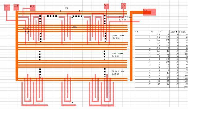
6 5 Test Chip description
7 6 PPI plating vendors Vendor A: completed pre-qualification Vendor B: could not meet specifications Vendor C: currently in pre-qualification Vendor A results are presented in subsequent slides
8 7 Vendor A results, as deposited Cu 30kA Al and 8kA Al WAT show the following: thick Cu to underlying Al capacitance is very well controlled, indicating good thickness uniformity of the planarized passivation (C_Area=350000um2) Thick Cu to the underlying Al leakage measured at 80V is well under 1nA (defectivity structure) Thick Cu sheet resistance is below ~1.5 mohm/[] Cu line to line leakage measured between the serpentine and the comb with the effective serp perimeter of ~15cm is < 10nA at 80V (or 0.1uA per cm2 of the serp sidewall area). Leakage yield loss is <1% 3X3 Via resistance (Kelvin method) is ~15mOhm

9 Rs of 20um Cu PPI Pattern Rs of PPI defect flat 20um Pattern ~9.5E-4 ohm/square Sample size: Rs of defect flat 20um Pattern 2.5E-03 TMAQ32 CHIP1 Defect Flat 20um I (A) 2007 TSMC, Ltd E-4 IV Rs E E E E E+00 V Rs of PPI defect flat 15um Pattern ~9.8E-4 ohm/square Sample size: 1100 Rs of defect flat 15um Pattern I (A) E-4 IV Rs v 2.50E E E E E E+00 Rs ( ohm /square ) Rs ( ohm /square ) Width:20um Space:20um Total length:78520um TMAQ32 CHIP1 Width:15um Space:15um Total length:69020um Defect Flat 15um
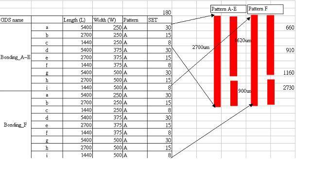
10 9 Vendor A results, wafer level stress Cu PPI exposed to ambient, clean required after the stress test prior to electrical testing. Temperature cycling, -65C to 150C, 1000 cycles Passed with no changes in parametrics and no cracks High Temperature Storage, 150C in air 5X5 via chains develop a higher R tail. This is not observed on Kelvin vias or on packaged via chains Un-biased HAST, 130C, 85% relative humidity 5X5 via chains develop a higher R tail. This is not observed on Kelvin vias or on packaged via chains
 and 0.18mm (1.8V/5V) BCD processes.")

11 10 Planarization and PPI effect on devices Planarized passivation with and w/o the PPI was applied to 0.25mm (2.5V/5V) and 0.18mm (1.8V/5V) BCD processes. Used 30kA and 8kA top Al for both processes Each device is partially covered by the PPI Less than 3% differences in parameter values observed PAD PPI Devise Device

12 11 Assembly issues Two assembly houses evaluated QFN-88 package with 0.8 mil Cu wire Both assembly houses demonstrated excellent bond-ability to Cu/Ni/Au both on flat features and over a sea of vias with specific design rules
13 12 Random assembly defects Defective units (QFN-88 not meeting the line-line leakage specification) FA Assembly house A Al particles Si particles (single occurrence) Ag particle Assembly houses A and B Stainless steel particle Cu particles C particle


14 13 Al particle (Assembly A): poorly maintained strip magazines and wafer carriers
: one time")
15 14 Si particle (Assembly A): one time occurrence


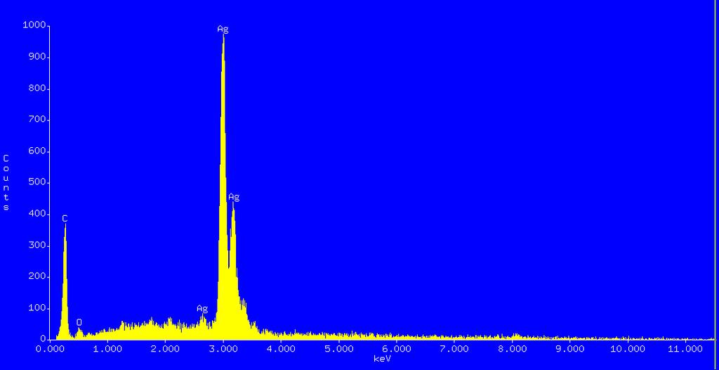
16 15 Ag particle (Assembly A, one time occurrence) OM SEM Ag
17 16 Systematic assembly defects 20mm and 15mm spaced Cu lines leakage improvement Stainless steel particles (~10% yield killer) Present in the molding compound Specified by vendor to be <130mm in size Limited potential for improvement Cu particles (~20% yield killer) Originate from the Cu deposit in scribe channels Can be eliminated by making sure Cu deposits are not present in scribe channels C cohesion particles (~70% yield killer) Improvement path identified by the molding compound vendor
18 17 Carbon cohesion particles improvement Defect size Current Dispersed Carbon Highly dispersed C Carbon 45um and > 22/ sample um-44um 40/sample um-24um 4/sample 3 2 Distribution of defect sizes for the current molding compound ( Current Carbon ), Dispersed Carbon and highly dispersed Carbon samples. Sumitomo formed two samples with each type of Carbon additive (10cm diameter disc, 2mm thick, weight ~31g), and inspected these for the black carbon particle number and size using the fluorescent microscope. Note that the dispersed and the highly dispersed Carbon grades result in significant reduction in the both the size and the observed density of C particles.
19 18 Package Level Reliability Tests Qualification Item Stress Condition Read Out Unbiased HAST T/ C Temperature Cycle HTS High Temperature Storage Test 130C / 85% RH / 33.3psi without bias -65C ~ +150C (Condition C, air to air) 150C 168 hrs 500 / 1000hrs 500 / 1000hrs
20 19 Summary and conclusions ~1 mohm/[] bond-able post passivation interconnect is developed Processing does not affect device parameters Several assembly defects are identified Assembly process/material items requiring improvement identified Effect on yield estimated PPI successfully pre-qualified Wafer level Package level
Project Proposal. Cu Wire Bonding Reliability Phase 3 Planning Webinar. Peng Su June 6, 2014
 Project Proposal Cu Wire Bonding Reliability Phase 3 Planning Webinar Peng Su June 6, 2014 Problem Statement Background Work of the inemi Cu wire reliability project identified that bonding quality and
Copper Wire Packaging Reliability for Automotive and High Voltage
 Copper Wire Packaging Reliability for Automotive and High Voltage Tu Anh Tran AMPG Package Technology Manager Aug.11.2015 TM External Use Agenda New Automotive Environments Wire Bond Interconnect Selection
12500 TI Boulevard, MS 8640, Dallas, Texas 75243
 12500 TI Boulevard, MS 8640, Dallas, Texas 75243 Add Cu as Alternative Wire Base Metal for Selected Device(s) Change Notification / Sample Request Date: 7/30/2015 To: Newark/Farnell PCN Dear Customer:
Chapter 4 Fabrication Process of Silicon Carrier and. Gold-Gold Thermocompression Bonding
 Chapter 4 Fabrication Process of Silicon Carrier and Gold-Gold Thermocompression Bonding 4.1 Introduction As mentioned in chapter 2, the MEMs carrier is designed to integrate the micro-machined inductor
23 rd ASEMEP National Technical Symposium
 THE EFFECT OF GLUE BOND LINE THICKNESS (BLT) AND FILLET HEIGHT ON INTERFACE DELAMINATION Raymund Y. Agustin Janet M. Jucar Jefferson S. Talledo Corporate Packaging & Automation/ Q&R STMicroelectronics,
Development of gold to gold interconnection flip chip bonding for chip on suspension assemblies
 Microelectronics Reliability 42 (2002) 381 389 www.elsevier.com/locate/microrel Development of gold to gold interconnection flip chip bonding for chip on suspension assemblies C.F. Luk a,1, Y.C. Chan b,
MATERIAL NEEDS AND RELIABILITY CHALLENGES IN AUTOMOTIVE PACKAGING UNDER HARSH CONDITIONS
 MATERIAL NEEDS AND RELIABILITY CHALLENGES IN AUTOMOTIVE PACKAGING UNDER HARSH CONDITIONS Varughese Mathew NXP Semiconductors 6501 William Cannon Drive, Austin TX, USA Automotive Innovation Driven by Electronics
TSV Interposer Process Flow with IME 300mm Facilities
 TSV Interposer Process Flow with IME 300mm Facilities Property of Institute of Microelectronics (IME)-Singapore August 17, 2012 Outline 1. TSV interposer (TSI) cross sectional schematic TSI with BEOL,
QUALIFICATION REPORT RELIABILITY LABORATORY
 QUALIFICATION REPORT RELIABILITY LABORATORY PCN #: IIRA-19WCBW841 Date: Jan 21, 2014 Qualification of 28L QFN (6x6x0.9mm) package at MTAI assembly site. The 28L QFN (5x5x0.9mm), 20L QFN (5x5x0.9mm, 4x4x0.9mm)
Cu Wire Bonding Survey Results. inemi Cu Wire Bonding Reliability Project Team Jan 30, 2011
 Cu Wire Bonding Survey Results inemi Cu Wire Bonding Reliability Project Team Jan 30, 2011 Outline About inemi Project Overview Survey Mechanism Survey Respondents Survey Results Technology Adoption Status
CMP for Thru-Silicon Vias TSV Overview & Examples March 2009
 CMP for Thru-Silicon Vias TSV Overview & Examples March 2009 Packaging Evolution Source: Yole Dev 2007 2 3D Integration Source: Yole Dev 2007 Growth rates for 3D integration Flash continues to drive the
PCN Title: Addition of New Fab/Assembly Site and Design Change
 DATE: 6 December 2016 PCN #: 2254 PCN Title: Addition of New Fab/Assembly Site and Design Change Dear Customer: This is an announcement of change(s) to products that are currently being offered by Diodes
Evaluation of Cu Pillar Chemistries
 Presented at 2016 IMAPS Device Packaging Evaluation of Cu Pillar Chemistries imaps Device Packaging Conference Spring 2016 Matthew Thorseth, Mark Scalisi, Inho Lee, Sang-Min Park, Yil-Hak Lee, Jonathan
CMOS Technology. Flow varies with process types & company. Start with substrate selection. N-Well CMOS Twin-Well CMOS STI
 CMOS Technology Flow varies with process types & company N-Well CMOS Twin-Well CMOS STI Start with substrate selection Type: n or p Doping level, resistivity Orientation, 100, or 101, etc Other parameters
The Development of a Novel Stacked Package: Package in Package
 The Development of a Novel Stacked Package: Package in Package Abstract Stacked die Chip Scale Packages (CSPs) or Fine-pitch BGAs (FBGAs) have been readily adopted and integrated in many handheld products,
800 W. 6 th Street, Austin, TX 78701
 800 W. 6 th Street, Austin, TX 78701 Assembly Site Transfer from StatsChipPac Kuala Lumpur, Malaysia (SCM) to ANST Wuxi CHINA for the CS8421-CNZ(R) component Process/Product Change Notification (Reference
800 W. 6 th Street, Austin, TX 78701
 800 W. 6 th Street, Austin, TX 78701 Assembly and Test Site Transfer from StatsChipPac Kuala Lumpur, Malaysia (SCM) to ANST Wuxi CHINA for the CS42L52-CNZ(R) and CS43L22-CNZ(R) components Process/Product
12500 TI Boulevard, MS 8640, Dallas, Texas 75243
 12500 TI Boulevard, MS 8640, Dallas, Texas 75243 Qualification of CLARK-AT as new assembly site for affected device(s) moving from SCSAT, corresponding package change from punched RTK to sawn RGP and change
Quality and Reliability Report
 Quality and Reliability Report Product Qualification MASW-007921 2mm 8-Lead Plastic Package QTR-0148 M/A-COM Technology Solutions Inc. 100 Chelmsford Street Lowell, MA 01851 Tel: (978) 656-2500 Fax: (978)
Hitachi Anisotropic Conductive Film ANISOLM AC-8955YW. Issued 2007/03/30
 Hitachi Chemical Data Sheet Hitachi Anisotropic Conductive Film ANISOLM AC-8955YW Issued 27/3/3 1. Standard specification, bonding condition, storage condition and characteristic...1 2. Precautions in
Wafer Level Molded DDFN Package Project Duane Wilcoxen
 Wafer Level Molded DDFN Package Project Duane Wilcoxen Definition of DDFN (Encapsulated CSP) DDFN package basically is a CSP device with an epoxy coating on all (or most) of the device sides for added
Quality and Reliability Report
 Quality and Reliability Report Product Qualification MAAM-008819 2mm 8-Lead PDFN Plastic Package QTR-0147 M/A-COM Technology Solutions Inc. 100 Chelmsford Street Lowell, MA 01851 Tel: (978) 656-2500 Fax:
The Shift to Copper Wire Bonding
 The Shift to Copper Wire Bonding E. Jan Vardaman President TechSearch International, Inc. www.techsearchinc.com 1/3/06 3/4/06 5/3/06 7/2/06 8/31/06 10/30/06 12/29/06 2/27/07 4/28/07 6/27/07 8/26/07 10/25/07
Innovative MID Plating Solutions
 Innovative MID Plating Solutions High Reliability Wire Bond Technique for MIDs Jordan Kologe MacDermid Electronics Solutions jkologe@macdermid.com 1 MacDermid: Specialty Chemical Solutions Over 2000 Worldwide
PRODUCT/PROCESS CHANGE NOTICE (PCN)
") 3545 North First Street San Jose, CA 95134 USA PRODUCT/PROCESS CHANGE NOTICE (PCN) PCN Number: 06-07 Date Issued: December 13, 2006 Product(s) Affected: Products using TQFN/TDFN type packages Manufacturing
3545 North First Street San Jose, CA 95134 USA PRODUCT/PROCESS CHANGE NOTICE (PCN) PCN Number: 06-07 Date Issued: December 13, 2006 Product(s) Affected: Products using TQFN/TDFN type packages Manufacturing
12500 TI Boulevard, MS 8640, Dallas, Texas 75243
 12500 TI Boulevard, MS 8640, Dallas, Texas 75243 PCN# 20121105000 Qualification of CLARK-AT as an additional Assembly Site for affected device(s) Change Notification / Sample Request Date: 11/7/2012 To:
II. A. Basic Concept of Package.
 Wafer Level Package for Image Sensor Module Won Kyu Jeung, Chang Hyun Lim, Jingli Yuan, Seung Wook Park Samsung Electro-Mechanics Co., LTD 314, Maetan3-Dong, Yeongtong-Gu, Suwon, Gyunggi-Do, Korea 440-743
Chips Face-up Panelization Approach For Fan-out Packaging
 Chips Face-up Panelization Approach For Fan-out Packaging Oct. 15, 2015 B. Rogers, D. Sanchez, C. Bishop, C. Sandstrom, C. Scanlan, TOlson T. REV A Background on FOWLP Fan-Out Wafer Level Packaging o Chips
12500 TI Boulevard, MS 8640, Dallas, Texas 75243
 12500 TI Boulevard, MS 8640, Dallas, Texas 75243 Qualification of CLARK-AT as new assembly site for affected device(s) moving from SCSAT, corresponding package change from punched RTK to sawn RGP and change
12500 TI Boulevard, MS 8640, Dallas, Texas 75243
 12500 TI Boulevard, MS 8640, Dallas, Texas 75243 Qualification of CLARK-AT as new assembly site for affected device(s) moving from SCSAT, corresponding package change from punched RSP to sawn RHH and associated
800 W. 6 th Street, Austin, TX 78701
 800 W. 6 th Street, Austin, TX 78701 Assembly and Test Site Transfer from StatsChipPac Kuala Lumpur, Malaysia (SCM) to ANST Wuxi CHINA for the CS42L52-CNZ(R) and CS43L22-CNZ(R) components Process/Product
Motorola MC68360EM25VC Communication Controller
 Construction Analysis EM25VC Communication Controller Report Number: SCA 9711-562 Global Semiconductor Industry the Serving Since 1964 17350 N. Hartford Drive Scottsdale, AZ 85255 Phone: 602-515-9780 Fax:
Analog, MEMS and Sensor Group (AMS)
") 05-13-2015 Report ID 2015-W20AMKOR-TRANSFER PRODUCT/PROCESS CHANGE NOTIFICATION PCN AMS/15/9324 Analog, MEMS and Sensor Group (AMS) Production transfer from Amkor Korea to Amkor Philippines for component
05-13-2015 Report ID 2015-W20AMKOR-TRANSFER PRODUCT/PROCESS CHANGE NOTIFICATION PCN AMS/15/9324 Analog, MEMS and Sensor Group (AMS) Production transfer from Amkor Korea to Amkor Philippines for component
Cypress Semiconductor Mold Compound Qualification Report
 Cypress Semiconductor Mold Compound Qualification Report QTP# 010601 VERSION 2.0 (G3) October 2004 28-44 Lead SOJ/20-32 Lead SOIC/28 Lead SNC s Sumitomo EME 6600HR Mold Compound, MSL3 Assembly CYPRESS
CPG (CMPG) Quality & Reliability Monitoring Program
 Quality & Reliability Monitoring Program") CPG (CMPG) Quality & Reliability Monitoring Program Quarterly Report Ending March 2018 DMS #PD-000190820 / DivDocID #129870 Microsemi s Commitment to You We at Microsemi s Communication Medical Products
CPG (CMPG) Quality & Reliability Monitoring Program Quarterly Report Ending March 2018 DMS #PD-000190820 / DivDocID #129870 Microsemi s Commitment to You We at Microsemi s Communication Medical Products
Description. Spectro Tabs, higher purity conductive carbon tabs,12mm O.D.
 Description SPEC The simplicity of application and smooth, clean surfaces of PELCO Tabs Carbon Conductive Tabs are a significant improvement compared to many of the other common adhesives that have been
Cu Bond Wire Reliability and Decapsulation Process
 CMSE Los Angeles April 12 th and 13 th, 2017 Cu Bond Wire Reliability and Decapsulation Process Sultan Ali Lilani - Integra Technologies LLC Ph 510-830-9216 Email: sultan.lilani@integra-tech.com Web: www.integra.com
800 W. 6 th Street, Austin, TX 78701
 800 W. 6 th Street, Austin, TX 78701 Assembly Site Transfer from StatsChipPac Kuala Lumpur, Malaysia (SCM) to ANST Wuxi CHINA for the CS8422-CNZ(R) component Process/Product Change Notification (Reference
SEMI Networking Day 2013 Rudolph Corporate Introduction
 SEMI Networking Day 2013 Rudolph Corporate Introduction Rudolph Technologies: Corporate Profile Business: Semiconductor capital equipment company dedicated exclusively to inspection, advanced packaging
EECS130 Integrated Circuit Devices
 EECS130 Integrated Circuit Devices Professor Ali Javey 9/13/2007 Fabrication Technology Lecture 1 Silicon Device Fabrication Technology Over 10 15 transistors (or 100,000 for every person in the world)
IME Technical Proposal. High Density FOWLP for Mobile Applications. 22 April High Density FOWLP Consortium Forum
 IME Technical Proposal High Density FOWLP for Mobile Applications 22 April 2014 Packaging driver for portable / mobile applications Key drivers/needs Smaller form-factor lower profile, substrate-less Higher
Deep Silicon Etching An Enabling Technology for Wireless Systems Segment By Carson Ogilvie and Joel Goodrich Commercial Product Solutions
 Deep Silicon Etching An Enabling Technology for Wireless Systems Segment By Carson Ogilvie and Joel Goodrich Commercial Product Solutions Abstract The recent installation of a new etch tool, the Surface
DS32KHZ 0.8um Fab Process 6" to 8" Conversion. Dallas Semiconductor
 1/5/27 RELIABILITY REPORT FOR DS32KHZ.8um Fab Process 6" to 8" Conversion Dallas Semiconductor 441 South Beltwood Parkway Dallas, TX 75244-3292 Prepared by: Ken Wendel Reliability Engineering Manager Dallas
Chapter 3 Silicon Device Fabrication Technology
 Chapter 3 Silicon Device Fabrication Technology Over 10 15 transistors (or 100,000 for every person in the world) are manufactured every year. VLSI (Very Large Scale Integration) ULSI (Ultra Large Scale
IMPLEMENTATION OF A FULLY MOLDED FAN-OUT PACKAGING TECHNOLOGY
 IMPLEMENTATION OF A FULLY MOLDED FAN-OUT PACKAGING TECHNOLOGY B. Rogers, C. Scanlan, and T. Olson Deca Technologies, Inc. Tempe, AZ USA boyd.rogers@decatechnologies.com ABSTRACT Fan-Out Wafer-Level Packaging
12500 TI Boulevard, MS 8640, Dallas, Texas 75243
 12500 TI Boulevard, MS 8640, Dallas, Texas 75243 PCN# 20121120000 Qualification of CLARK-AT as new assembly site for affected device(s) moving from SCSAT, corresponding package change from punched RSP
Packaging Commercial CMOS Chips for Lab on a Chip Integration
 Supporting Information for Packaging Commercial CMOS Chips for Lab on a Chip Integration by Timir Datta-Chaudhuri, Pamela Abshire, and Elisabeth Smela Biocompatibility Although the supplier s instructions
Overview of CMP for TSV Applications. Robert L. Rhoades, Ph.D. Presentation for AVS Joint Meeting June 2013 San Jose, CA
 Overview of CMP for TSV Applications Robert L. Rhoades, Ph.D. Presentation for AVS Joint Meeting June 2013 San Jose, CA Outline TSV s and the Role of CMP TSV Pattern and Fill TSV Reveal (non-selective)
S/C Packaging Assembly Challenges Using Organic Substrate Technology
 S/C Packaging Assembly Challenges Using Organic Substrate Technology Presented by Bernd Appelt ASE Group Nov. 17, 2009 Overview The Packaging Challenge Chip Substrate Interactions Stiffeners for FC-BGA
SLIM TM, High Density Wafer Level Fan-out Package Development with Submicron RDL
 2017 IEEE 67th Electronic Components and Technology Conference SLIM TM, High Density Wafer Level Fan-out Package Development with Submicron RDL YoungRae Kim 1, JaeHun Bae 1, MinHwa Chang 1, AhRa Jo 1,
Cu-Al intermetallic growth behaviour study under high temperature thermal aging
 Cu-Al intermetallic growth behaviour study under high temperature thermal aging C.L Cha, H.J Chong, Yaw HG, Chong MY, Teo CH Infineon Technologies, Melaka, Malaysia Abstract Copper (Cu) wire always gains
TGV and Integrated Electronics
 TGV and Integrated Electronics Shin Takahashi ASAHI GLASS CO., LTD. 1 Ambient Intelligence Green Energy/Environment Smart Factory Smart Mobility Smart Mobile Devices Bio/Medical Security/Biometrics 2 Glass
Report Title: ADSP-BF538F8 /ADSP-BF539F8 Alternate Fab Site Qualification
 Report Title: ADSP-BF538F8 /ADSP-BF539F8 Alternate Fab Site Qualification Report Number: 9127 Revision: Date: 15 April 2011 A Summary Reliability Report: 9127 This report documents the successful completion
12500 TI Boulevard, MS 8640, Dallas, Texas 75243
 12500 TI Boulevard, MS 8640, Dallas, Texas 75243 PCN# 20130708002 Qualification of TI Clark as an Additional Assembly, Bump, and Test site for Select Devices on WCSP and QFN Package Change Notification
Product Change Notification - JAON-14OICS710 (Printer Friendly)
") Product Change Notification - JAON-14OICS710-17 Oct 2016 - CCB 2697 Final Notice... http://www.microchip.com/mymicrochip/notificationdetails.aspx?pcn=jaon-14oics710 Page 1 of 3 10/18/2016 English Search...
Product Change Notification - JAON-14OICS710-17 Oct 2016 - CCB 2697 Final Notice... http://www.microchip.com/mymicrochip/notificationdetails.aspx?pcn=jaon-14oics710 Page 1 of 3 10/18/2016 English Search...
Characterization of 0.6mils Ag Alloy Wire in BGA Package
 Characterization of 0.6mils Ag Alloy Wire in BGA Package Toh Lee Chew, Alan Lumapar Visarra, *Fabien Quercia, *Eric Perriaud STMicroelectronics Muar, Tanjung Agas Industrial, P.O.Box 28, 84007, Muar, Johor
Next Gen Packaging & Integration Panel
 Next Gen Packaging & Integration Panel ECTC 2012 Daniel Tracy, Sr. Director Industry Research & Statistics SEMI May 29, 2012 Packaging Supply Chain Market Trends Material Needs and Opportunities Market
1.1 Background Cu Dual Damascene Process and Cu-CMP
 Chapter I Introduction 1.1 Background 1.1.1 Cu Dual Damascene Process and Cu-CMP In semiconductor manufacturing, we always directed toward adding device speed and circuit function. Traditionally, we focused
MEPTEC Semiconductor Packaging Technology Symposium
 MEPTEC Semiconductor Packaging Technology Symposium Advanced Packaging s Interconnect Technology Process Shift and Direction October 23, 2014 Jay Hayes- Director of Business Development -Bumping and Flip
Evaluation of Copper CMP Process Characterization Wafers
 SKW Associates, Inc. Evaluation of Copper CMP Process Characterization Wafers SKW6-3 & SKW6-5 SooKap Hahn Jan 15, 2005 Polish Proposal 1 Planned Polishing: Week of Dec 20 th Customer: SKW Associates Inc.
GaN on Si Manufacturing Excellency in CMOS Foundry Fab
 GaN on Si Manufacturing Excellency in CMOS Foundry Fab Paul Chu Oct. 2016 Agenda 1. GaN Device Offering 2. GaN Production 3. GaN MoCVD Manufacturability 4. Yield Improvement 5. Summary 2 l GaN superiority
Qualification Report. PALCE16V8 (Flash Erasable, Reprogramable CMOS PAL ) April 1996, QTP# 96023, Version 1.0
 April 1996, QTP# 96023, Version 1.0") Qualification Report April 1996, QT# 96023, Version 1.0 ALCE16V8 (Flash Erasable, Reprogramable CMOS AL ) AL is registered trademark of Advanced Micro Devices, Inc. RODUCT DESCRITION (for qualification)
Qualification Report April 1996, QT# 96023, Version 1.0 ALCE16V8 (Flash Erasable, Reprogramable CMOS AL ) AL is registered trademark of Advanced Micro Devices, Inc. RODUCT DESCRITION (for qualification)
Development and Characterization of 300mm Large Panel ewlb (embedded Wafer Level BGA)
") Development and Characterization of 300mm Large Panel ewlb (embedded Wafer Level BGA) Seung Wook Yoon, Yaojian Lin and Pandi C. Marimuthu STATS ChipPAC Ltd. 5 Yishun Street 23, Singapore 768442 E-mail
Development and Characterization of 300mm Large Panel ewlb (embedded Wafer Level BGA) Seung Wook Yoon, Yaojian Lin and Pandi C. Marimuthu STATS ChipPAC Ltd. 5 Yishun Street 23, Singapore 768442 E-mail
2015 EE410-LOCOS 0.5µm Poly CMOS Process Run Card Lot ID:
 STEP 0.00 - PHOTOMASK #0- ZERO LEVEL MARKS Starting materials is n-type silicon (5-10 ohm-cm). Add four test wafers labeled T1-T4. T1 and T2 will travel with the device wafers and get all of the processing
Notable Trends in CMP: Past, Present and Future
 Notable Trends in CMP: Past, Present and Future Semiconductor International February 15 th, 2007 Pete Singer Editor-in-Chief Levitronix CMP Users Conference 2007 April 1988: Etchback, SOG November 1990:
TSV Processing and Wafer Stacking. Kathy Cook and Maggie Zoberbier, 3D Business Development
 TSV Processing and Wafer Stacking Kathy Cook and Maggie Zoberbier, 3D Business Development Outline Why 3D Integration? TSV Process Variations Lithography Process Results Stacking Technology Wafer Bonding
Copper Power Pad Design Challenges for Robust and High Energy Efficient Packages
 Copper Power Pad Design Challenges for Robust and High Energy Efficient Packages Hoe Jian Chong, Jeramie Dimatira ON Semiconductor, SCG Industries (M) Sdn. Bhd. Lot 122, Senawang Industrial Estate, 70450
Qualification Report. June, 1994, QTP# Version 1.1 CY7C46X/47X, MINNESOTA FAB MARKETING PART NUMBER DEVICE DESCRIPTION. Cascadable 32K x 9 FIFO
 Qualification Report June, 1994, QTP# 92361 Version 1.1 CY7C46X/47X, MINNESOTA FAB MARKETING PART NUMBER CY7C460 CY7C462 CY7C464 CY7C470 CY7C472 CY7C474 DEVICE DESCRIPTION Cascadable 8K x 9 FIFO Cascadable
JOINT INDUSTRY STANDARD
 JOINT INDUSTRY STANDARD AUGUST 1999 Semiconductor Design Standard for Flip Chip Applications ASSOCIATION CONNECTING ELECTRONICS INDUSTRIES Semiconductor Design Standard for Flip Chip Applications About
Anisotropic Conductive Films (ACFs)
") Anisotropic Conductive Films (ACFs) ACF = Thermosetting epoxy resin film + Conductive particles Chip or substrate 1 Heat Pressure ACF Substrate 2 Chip or substrate 1 ACF Substrate 2 Applications Chip-on-Board
Anisotropic Conductive Films (ACFs) ACF = Thermosetting epoxy resin film + Conductive particles Chip or substrate 1 Heat Pressure ACF Substrate 2 Chip or substrate 1 ACF Substrate 2 Applications Chip-on-Board
Simulations and Characterizations for Stress Reduction Designs in Wafer Level Chip Scale Packages
 Simulations and Characterizations for Stress Reduction Designs in Wafer Level Chip Scale Packages by Ming-Che Hsieh STATS ChipPAC Taiwan Co. Ltd. Copyright 2013. Reprinted from 2013 International Microsystems,
SE2618F with Cu wire at Carsem Package Qualification Plan
 SE2618F with Cu wire at Carsem Package Qualification Plan Part Number: SE2618F with Cu wire Product Type: 2.4GHz 802.11b/g/n WLAN FEM Package Type: QFN 2.5 x 2.5 x 0.45mm 16L Report No: Qual-QP-12-01106
Nanium Overview. Company Presentation
 Nanium Overview Company Presentation Nanium Overview Our name and logo nano prefix of Greek origin referring to small objects ium suffix of Latin origin that includes the formation of scientific terms
Plasma Etching Rates & Gases Gas ratios affects etch rate & etch ratios to resist/substrate
 Plasma Etching Rates & Gases Gas ratios affects etch rate & etch ratios to resist/substrate Development of Sidewalls Passivating Films Sidewalls get inert species deposited on them Creates passivating
A study aimed at characterizing the interfacial structure in a tin silver solder on nickel-coated copper plate during aging
 Sādhanā Vol. 33, Part 3, June 2008, pp. 251 259. Printed in India A study aimed at characterizing the interfacial structure in a tin silver solder on nickel-coated copper plate during aging D C LIN 1,
WorkShop Audace. INSA ROUEN 8 juin 2012
 WorkShop Audace INSA ROUEN 8 juin 2012 Global Standards for the Microelectronics Industry JEDEC standards for product level qualification Christian Gautier Content JEDEC overview Environmental reliability
FINAL PRODUCT/PROCESS CHANGE NOTIFICATION Generic Copy. 11-Apr SUBJECT: ON Semiconductor Final Product/Process Change Notification #15507
 FINAL PRODUCT/PROCESS CHANGE NOTIFICATION Generic Copy 11-Apr-26 SUBJECT: ON Semiconductor Final Product/Process Change Notification #1557 TITLE: Qualification of OSPI for Assembly/Test of 8/14/16 Lead
CX Thin Fil s. Resistors Attenuators Thin-Film Products Thin-Film Services. ISO 9001:2008 RoHS/REACH Compliant ITAR Compliant
 CX Thin Fil s Resistors Attenuators Thin-Film Products Thin-Film Services www.cxthinfilms.com ISO 9001:2008 RoHS/REACH Compliant ITAR Compliant www.cxthinfilms.com sales@cxthinfilms.com +1 (401) 461-5500
Product Change Notification - JAON-07LFEV539 (Printer Friendly)
") Product Change Notification - JAON-07LFEV539-28 Nov 2016 - CCB 2695 and 2695.0... http://www.microchip.com/mymicrochip/notificationdetails.aspx?pcn=jaon-07lfev539 Page 1 of 3 11/29/2016 English Search...
Product Change Notification - JAON-07LFEV539-28 Nov 2016 - CCB 2695 and 2695.0... http://www.microchip.com/mymicrochip/notificationdetails.aspx?pcn=jaon-07lfev539 Page 1 of 3 11/29/2016 English Search...
EE 143 CMOS Process Flow
 EE 143 CMOS rocess Flow CT 84 D D G Sub G Sub S S G D S G D S + + + + - MOS Substrate Well - MOS Substrate EE 143 CMOS rocess Flow CT 85 hotoresist Si 3 4 SiO 2 Substrate selection: moderately high resistivity,
Process Change Notice #
 User Registration Register today to create your account on Silabs.com. Your personalized profile allows you to receive technical document updates, new product announcements, how-to and design documents,
IPC RELIABILITY - CASTELLETTO. Reliability Report. Combo IC for PFC and ballast control Assembly plant location
 General Information Locations Product Line Product Description Product division U337 Combo IC for PFC and ballast control I&PC Wafer fab location Assembly plant location ANG MO KIO MUAR Package SO20 Silicon
Novel Solutions for ESD Sensitive Devices
 Novel Solutions for ESD Sensitive Devices Chris Schreiber Magnecomp cschreiber@magnecomp.com Safely Dissipating ESD Problem Static Charging is created by either Tribocharging or Induction and the uncontrolled
PCN Title: Change of Assembly Materials, Assembly Process and Mechanical Specification
 DATE: 7 December, 2016 PCN #: 2250 PCN Title: Change of Assembly Materials, Assembly Process and Mechanical Specification Dear Customer: This is an announcement of change(s) to products that are currently
Plasma Etching Rates & Gases Gas ratios affects etch rate & etch ratios to resist/substrate
 Plasma Etching Rates & Gases Gas ratios affects etch rate & etch ratios to resist/substrate Development of Sidewalls Passivating Films Sidewalls get inert species deposited on them with plasma etch Creates
12500 TI Boulevard, MS 8640, Dallas, Texas 75243
 12500 TI Boulevard, MS 8640, Dallas, Texas 75243 Qualification of TIEM (Melaka, MLA) as an Additional Assembly and Test Site option for select devices in the DCQ package Change Notification Date: March
Power Electronics Packaging Solutions for Device Junction Temperature over 220 o C
 EPRC 12 Project Proposal Power Electronics Packaging Solutions for Device Junction Temperature over 220 o C 15 th August 2012 Page 1 Motivation Increased requirements of high power semiconductor device
Embedded Passives..con0nued
 Embedded Passives..con0nued Why Embedded Passives? Improves the packaging efficiency System-on-Package (SOP); SLIM integration Reducing size Eliminating substrate assembly Minimizing solder joint failure
QFN Challenges: Second Bond Improvement to Eliminate the Weak Stitch (Fish Tail) Failure Mechanism on Pre Plated Lead Frame
 Failure Mechanism on Pre Plated Lead Frame") QFN Challenges: Second Bond Improvement to Eliminate the Weak Stitch (Fish Tail) Failure Mechanism on Pre Plated Lead Frame Jacky Lee Sinn Fah, Sreetharan Sekaran, Rameish Rao Subarmaniyan Central Process
QFN Challenges: Second Bond Improvement to Eliminate the Weak Stitch (Fish Tail) Failure Mechanism on Pre Plated Lead Frame Jacky Lee Sinn Fah, Sreetharan Sekaran, Rameish Rao Subarmaniyan Central Process
12500 TI Boulevard, MS 8640, Dallas, Texas 75243
 12500 TI Boulevard, MS 8640, Dallas, Texas 75243 Qualification of RFAB as an additional FAB site option for selected devices in the C05 Process Change Notification Date: 8/15/2012 To: MOUSER PCN Dear Customer:
Material based challenge and study of 2.1, 2.5 and 3D integration
 1 Material based challenge and study of 2.1, 2.5 and 3D integration Toshihisa Nonaka Packaging Solution Center R&D Headquarters Hitachi Chemical Co., Ltd., Sep. 8, 2016 Hitachi Chemical Co., Ltd. 2010.
The Packaging and Reliability Qualification of MEMS Resonator Devices
 The Packaging and Reliability Qualification of MEMS Resonator Devices Pavan Gupta Vice President, Operations Yin-Chen Lu, Preston Galle Quartz and MEMS Oscillators source: www.ecliptek.com Quartz Oscillators:
The 3D Silicon Leader. Company Presentation. SMTA Houston, 14th March 2013
 The 3D Silicon Leader Company Presentation SMTA Houston, 14th March 2013 Who are we? Independent Company located in Caen, Normandy, France Dedicated to manufacturing of leading edge Integrated Passive
Rockwell R RF to IF Down Converter
 Construction Analysis Rockwell R6732-13 RF to IF Down Converter Report Number: SCA 9709-552 Global Semiconductor Industry the Serving Since 1964 17350 N. Hartford Drive Scottsdale, AZ 85255 Phone: 602-515-9780
PIL Product/Process Information Letter
 STMicroelectronics IPD - ASD & IPAD Division 1 BU Rectifiers (1) IPD: Industrial & Power Discretes - ASD: Application Specific Device IPAD : Integrated Passive and Active Devices PIL Product/Process Information
RELIABILITY TEST RESULTS
 RELIABILITY TEST RESULTS High Temperature Storage (125 C) The High Temperature Storage test was performed to accelerate failure mechanisms that are primarily thermally activated (such as ionic diffusion
RELIABILITY EVALUATION QUALIFICATION OF SOIC8L Narrow & SOIC8L E-PAD XDLF-IDF (EXTREAM DENSITY LEAD FRAME) ATP1 (AMKOR PHILIPPINES SUBCON)
 ATP1 (AMKOR PHILIPPINES SUBCON)") AMG Analog & Mems -Group Industrial & Power Conversion Div. Quality & Reliability B-END RR000116CT6004 RELIABILITY EVALUATION QUALIFICATION OF SOIC8L Narrow & SOIC8L E-PAD XDLF-IDF (EXTREAM DENSITY LEAD
AMG Analog & Mems -Group Industrial & Power Conversion Div. Quality & Reliability B-END RR000116CT6004 RELIABILITY EVALUATION QUALIFICATION OF SOIC8L Narrow & SOIC8L E-PAD XDLF-IDF (EXTREAM DENSITY LEAD
NKK NR4645LQF Bit RISC Microprocessor
 Construction Analysis NKK NR4645LQF-133 64-Bit RISC Microprocessor Report Number: SCA 9707-547 Global Semiconductor Industry the Serving Since 1964 17350 N. Hartford Drive Scottsdale, AZ 85255 Phone: 602-515-9870
DEC SA-110S StrongARM 32-Bit Microprocessor
 Construction Analysis DEC SA-110S StrongARM 32-Bit Microprocessor Report Number: SCA 9704-535 Global Semiconductor Industry the Serving Since 1964 15022 N. 75th Street Scottsdale, AZ 85260-2476 Phone:
PCN Title: Additional FAB Source (TPSCo), Additional Assembly/Test Site (SAT) and BOM (Bill of Materials) on select devices
, Additional Assembly/Test Site (SAT) and BOM (Bill of Materials) on select devices") DATE: 18 th July, 2016 PCN #: 2239 PCN Title: Additional FAB Source (TPSCo), Additional Assembly/Test Site (SAT) and BOM (Bill of Materials) on select devices Dear Customer: This is an announcement of
DATE: 18 th July, 2016 PCN #: 2239 PCN Title: Additional FAB Source (TPSCo), Additional Assembly/Test Site (SAT) and BOM (Bill of Materials) on select devices Dear Customer: This is an announcement of