Integration and Packaging
|
|
|
- Mervyn Cummings
- 5 years ago
- Views:
Transcription

1 Workshop on Smart Systems for Healthcare and Wellness Brusselles Hosted by the CATRENE Scientific Committee Integration and Packaging Erik Jung, Harald Pötter


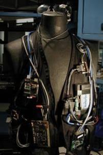
2 Medical Innovations.. and requirements Medical technology uses micro devices already as components (ASICs, power ICs, accelerometers, pressure sensors) Typically well known and understood technologies and components (risk minimization) are used Innovative components and technologies need to prove both function and robustness prior integration into a system which again needs to prove funtion and robustness as a whole Mechanical design more difficult under DfM constraints than pure electronic design Medical devices operate under conditions, which cannot be controlled by the manufacturer -> can result in very individual requirements (surgeon s skill, patient behaviour) -> sluggish adoption of novel integration and packaging technogies into the medical market
3 Technologies from MST which lend themselves for the medical arena Component Development Low Power ASICs Sensor devices Power supply Component enhancement Functionalization Rewiring, TSV Level Zero Advanced Substrate Technology 3D Flex MID/MDD, Textiles Surface Modifications Micro Assembly and Encapsulation Heterointegration in 3D Ultrasmall form factor assembly Mechanical Protective Layer Silicone biocompatibility layer Barrier Layer Deposition Parylene conformal coating DLC deposition ALD of Al2O3 Functional Layer Deposition PEG, DEL, HAD 3D Free Form Generation Rapid prototyping/manufacturing Embedded electronic funtionality
4 Technologies from MST which lend themselves for the medical arena Component Development Low Power ASICs Sensor devices Power supply Component enhancement Functionalization Rewiring, TSV Level Zero Advanced Substrate Technology 3D Flex MID/MDD, Textiles Surface Modifications Micro Assembly and Encapsulation Heterointegration in 3D Ultrasmall form factor assembly Mechanical Protective Layer Component enhancement Functionalization Rewiring, TSV Silicone biocompatibility layer Barrier Layer Deposition Parylene conformal coating DLC deposition ALD of Al2O3 Level Zero Functional Layer Deposition PEG, DEL, HAD 3D Free Form Generation Rapid prototyping/manufacturing Embedded electronic funtionality
5


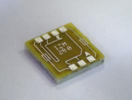
6 SiP modules with embedded SAW filters CSSP Cu frame 1.4x1.1x0.4mm 5 contacts Ni/Au DSSP 0.95mmx0.6mmx0.21mm 6 contacts lead-free bumps Assembly DSSP&CSSP Cross section of module 4mmx4mmx0.91mm Embedding feasible( ) EPCOS testing ( )


 M2")

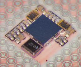
7 3D-SiP Design / Layout LETI - antenna VTT - antenna Antenna - footprint Piezo - Module module to module - footprint (14 pins) M2 assembly-layer SoC - module SiP footprint (31 pins) M1 assembly-layer
8 3D-SiP Stacking Concept optimized for the interconnections between SoC and Device PCB shortest possible way for antenna path copper thickness on surface: 20µm Antenna Module thickness: 600µm gap between soldermasks: <30µm Solder Mask (20µm) Antenna Path Copper thickness in via: 15-20µm SoC - Module <1,13mm Interconnection to PCB Device PCB
9 Technologies from MST which lend themselves for the medical arena Component Development Low Power ASICs Sensor devices Power supply Component enhancement Functionalization Rewiring, TSV Level Zero Advanced Substrate Technology 3D Flex MID/MDD Surface Modifications Micro Assembly and Encapsulation Heterointegration Ultrasmall form factor assembly Micro Assembly and Encapsulation Heterointegration in 3D Mechanical Protective Layer Silicone biocompatibility layer Barrier Layer Deposition Ultrasmall form factor assembly Parylene conformal coating Mechanical Protective Layer DLC deposition ALD of Al2O3 Silicone biocompatibility layer Functional Layer Deposition PEG, DEL, HAD 3D Free Form Generation Rapid prototyping/manufacturing Embedded electronic funtionality

10 Cooperation with AWAIBA and SUSS resulted in world record in integrated camera system Assembly on 1,5m long miniature flex substrate strip (roll-roll fabrication)


11 Novel diagnostic applications using miniature electronic optics and flex integration Endoscope camera, ultrasmall Combining microelectronic CMOS imaging chip with microoptical lenses MEMS bonding technologies Microbumps for attachment to flex

12 Cooperation with AWAIBA and SUSS resulted in world record in integrated camera system.and going stereo by just adjusting the dicing pattern!


13 Chip-on-Board Stacking Technology signal processing ASIC photo diodes courtesy of Swissbit Germany PCB controller EMC shielding Stacked devices assembled in COB technology Wire bonding at different device levels (1mil AlSi1) S. Schmitz


14 Flip Chip Technologies Thermode Bonding Thermocompression Thermosonic Reflow soldering Adhesive Joining ICA - Isotropic Conductive Adhesive NCA - Non Conductive Adhesive ACA - Anisotropic Conductive Adhesive SnAg Au stud

15 Ultra Thin Flip Chip Interconnects B. Pahl, C. Kallmayer


16 Thin Chip integration: Reliable System Level Integration of Stacked Chips on MEMS FC embedded chip RDL wafer cross section of a three chip stack using chip embedding: thin chip embedded on wafer, formation of a RDL, FC-Bonding Top view Bumped TCI on wafer level Chip scale package integration of different microsystem technologies by thin die stacking, polymer embedding and redistribution/bumping


17 Combining TSV, µassembly and thin film routing for next generation medical devices Substrate with thin film wiring and through silicon/glass vias Medtronic s vision of chip scale pacemaker µassembly of MEMS and thinned components by die-stacking Wafer level hermetic sealing
18 Technologies from MST which lend themselves for the medical arena Component Development Ultrasmall form factor assembly Low Power ASICs Sensor devices Power supply Component enhancement Functionalization Rewiring, TSV Level Zero Advanced Substrate Technology Micro Assembly and Encapsulation Heterointegration Mechanical Protective Layer Advanced Substrate Technology 3D Flex MID/MDD Textiles Surface Modifications Silicone biocompatibility layer Barrier Layer Deposition Parylene conformal coating DLC deposition ALD of Al2O3 Functional Layer Deposition PEG, DEL, HAD 3D Flex 3D Free Form Generation MID/MDD Rapid prototyping/manufacturing Surface Modifications Embedded electronic funtionality


19 From rigid to flexible systems MIT Novanex/Sonago stretchable flexible rigid


20 Motivation Enabling potential of thermoplastic substrates Polycarbonate: high reliability flexible high threshold for plastic deformation Chemical sensitivity Polyurethane: flexible & stretchable Good adhesion to many surfaces Low melting temperature
21 Flexible and Stretchable Substrates Properties PI LCP PET PC TPU Tensile Strength [MPa] ~ Modulus [MPa] Dielectric constant >3 T g [ C] 230 T melt : T melt : T mel : CTE [ppm] < T g (with filler) 70 (unfilled) ~200 Moisture uptake [%] < Breakthrough voltage [kv/mm] Via size [µm] 200 µvia: µvia: Min. Line/Space* Maturity of technology standard low volume Standard R&D R&D, transferred to few manufacturers


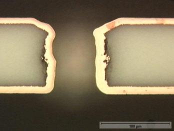
22 Structuring of Thermoplastic Substrates Via in Polycarbonate foil Via in thermoplastic polyurethane foil
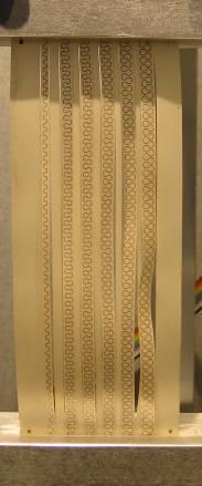
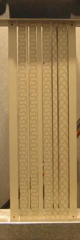
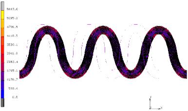
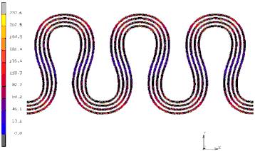
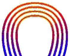
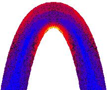
23 Stretchable Circuit Board Cu track patterning Cyclic stretching: reliability


24 Stretchable Circuit Board Rigid stretch transition meanders for Stretchablility local Cu Stiffeners bondpads for components


25 Ultrathin Chips for flexible Electronics Necessity of ultrathin chips: mechanical flexibility thin modules 3D-integration Reasons for component integration in substrate: fine pitch high density, short paths thin modules with flat surface Prerequisites: commercial availability of thin chips qualified assembly processes with ultrathin contacs


26 Integration Technologies: Thermode Bonding Application of adhesive or noflow underfill Curing / soldering under temperature and presure 450 µm Chip 20 µm Chip 450 µm Chip 20 µm Chip X-Ray of SMX after ACA bonding


27 Application Example: Diagnostic Band Aid Stretchable substrate + encapsulation for the electronic compontes control LED photodetector read out electronic Skin tissue color markers opt. excitation flourescence

28 Application Example: T-Shirt for Muscle Stimulation Therapy System design: Uni Boras* Functionality: Muscle stimulation therapy for patients with muscle spasticity SCB for interconnection between dry electrodes distributed over the shirt Interconnection to electrodes with push buttons F. Seoane, STRETCHABLE CIRCUIT BOARD TECHNOLOGY ENABLING SEAMLESS TEXTILE-ELECTRONIC INTEGRATION FOR ELECTRICAL MUSCLE STIMULATION THERAPY, Printed Electronics USA, 2012


29 Application Example: Implantable Electrodes for Neural Interconnection e-nerve Process flow with Au metallization Nanostructured Au surface Improved cell adhesion Increased surface
30 Synopsis Micro electronics and micro system technology offer new opportunities to use innovative techniques and convert them into novel products. New and improved diagnostic and therapeutic concepts can be realized by leveraging these technologies The synergy between the medical sector, micro electronics, microintegration and IT will offer improved quality of life now and in the future at acceptable cost due to the economy of scale and high degrees of autonomy enabled by these advancements Nano scale sensors will allow to increase functionality of diagnostic methods significantly micro-packaging will play a strong role here for final integration into a product

31 For further information please contact Erik Jung
Microtechnology for the HighTec Medical Industry -micro packaging as an enabler for next generation devices-
 Microtechnology for the HighTec Medical Industry -micro packaging as an enabler for next generation devices- Erik Jung, Fraunhofer IZM Erik.jung@izm.fraunhofer.de Technologies from MST which lend themselves
Flexible Substrates for Smart Sensor Applications
 Flexible Substrates for Smart Sensor Applications A novel approach that delivers miniaturized, hermetic, biostable and highly reliable smart sensor modules. AUTHORS Dr. Eckardt Bihler, Dr. Marc Hauer,
5. Packaging Technologies Trends
 5. Packaging Technologies Trends Electronic products and microsystems continue to find new applications in personal, healthcare, home, automotive, environmental and security systems. Advancements in packaging
Fraunhofer IZM. All Silicon System Integration Dresden Scope. M. Juergen Wolf
 Fraunhofer IZM All Silicon System Integration Dresden Scope M. Juergen Wolf Fraunhofer IZM All Silicon System Integration - ASSID Dresden, Berlin, Germany Fraunhofer IZM Focus of Activities Materials,
3D-IC Integration using D2C or D2W Alignment Schemes together with Local Oxide Reduction
 3D-IC Integration using D2C or D2W Alignment Schemes together with Local Oxide Reduction Gilbert Lecarpentier*, Jean-Stéphane Mottet* SET S.A.S. (Smart Equipment Technology), 131 Impasse Barteudet, 74490
Challenges for Embedded Device Technologies for Package Level Integration
 Challenges for Embedded Device Technologies for Package Level Integration Kevin Cannon, Steve Riches Tribus-D Ltd Guangbin Dou, Andrew Holmes Imperial College London Embedded Die Technology IMAPS-UK/NMI
Stretchable electronics
 Stretchable electronics Constraints and possibilities for direct printing on thermoplastic polyurethanes From flexible printed electronics to stretchable Eric Rubingh, Corné Rentrop, Piet Bouten < 3 Holst
YOUR Strategic TESTING ENGINEERING CONCEPT SMT FLIP CHIP PRODUCTION OPTO PACKAGING PROCESS DEVELOPMENT CHIP ON BOARD SUPPLY CHAIN MANAGEMENT
 YOUR Strategic TECHNOLOGY PARTNER Wafer Back-End OPTO PACKAGING PROCESS DEVELOPMENT CONCEPT FLIP CHIP PROTOTYping ENGINEERING TESTING SMT PRODUCTION CHIP ON BOARD SUPPLY CHAIN MANAGEMENT Next Level 0f
Cu Pillar Interconnect and Chip-Package-Interaction (CPI) for Advanced Cu Low K chip
 for Advanced Cu Low K chip") EPRC 12 Project Proposal Cu Pillar Interconnect and Chip-Package-Interaction (CPI) for Advanced Cu Low K chip 15 th Aug 2012 Page 1 Introduction: Motivation / Challenge Silicon device with ultra low k
EPRC 12 Project Proposal Cu Pillar Interconnect and Chip-Package-Interaction (CPI) for Advanced Cu Low K chip 15 th Aug 2012 Page 1 Introduction: Motivation / Challenge Silicon device with ultra low k
Recent Advances in Die Attach Film
 Recent Advances in Die Attach Film Frederick Lo, Maurice Leblon, Richard Amigh, and Kevin Chung. AI Technology, Inc. 70 Washington Road, Princeton Junction, NJ 08550 www.aitechnology.com Abstract: The
Smart Implants: Packaging Challenges & Solutions. inemi-2010 Berlin TCl/JFZ
 Smart Implants: Packaging Challenges & Solutions Topics 1. Smart Implants and Packaging Challenges 2. Enabling Miniaturisation Processes 3. Successfully Deployed Examples at Valtronic Group What is a Smart
iniaturization of medical devices thanks to flexible substrates ISO 9001 certified
 iniaturization of medical devices thanks to flexible substrates 04-12-2012 Hightec MC Presentation 2 Medical industry is clearly and urgently in need of the development of advanced interconnection solutions
YOUR Strategic TESTING ENGINEERING CONCEPT SMT FLIP CHIP PRODUCTION OPTO PACKAGING PROCESS DEVELOPMENT CHIP ON BOARD SUPPLY CHAIN MANAGEMENT
 YOUR Strategic TECHNOLOGY PARTNER Wafer Back-End OPTO PACKAGING PROCESS DEVELOPMENT CONCEPT FLIP CHIP PROTOTYping ENGINEERING TESTING SMT PRODUCTION CHIP ON BOARD SUPPLY CHAIN MANAGEMENT Next Level 0f
New Technology for High-Density LSI Mounting in Consumer Products
 New Technology for High-Density Mounting in Consumer Products V Hidehiko Kira V Akira Takashima V Yukio Ozaki (Manuscript received May 29, 2006) The ongoing trend toward downsizing and the growing sophistication
Chapter 3 Silicon Device Fabrication Technology
 Chapter 3 Silicon Device Fabrication Technology Over 10 15 transistors (or 100,000 for every person in the world) are manufactured every year. VLSI (Very Large Scale Integration) ULSI (Ultra Large Scale
Chapter 4 Fabrication Process of Silicon Carrier and. Gold-Gold Thermocompression Bonding
 Chapter 4 Fabrication Process of Silicon Carrier and Gold-Gold Thermocompression Bonding 4.1 Introduction As mentioned in chapter 2, the MEMs carrier is designed to integrate the micro-machined inductor
3DIC Integration with TSV Current Progress and Future Outlook
 3DIC Integration with TSV Current Progress and Future Outlook Shan Gao, Dim-Lee Kwong Institute of Microelectronics, A*STAR (Agency for Science, Technology and Research) Singapore 9 September, 2010 1 Overview
Fraunhofer IZM Bump Bonding and Electronic Packaging
 Fraunhofer IZM Bump Bonding and Electronic Packaging Fraunhofer Institute for Reliability and Microintegration (IZM) Gustav-Meyer-Allee 25 13355 Berlin Germany Dipl.-Ing. Thomas Fritzsch Contact: thomas.fritzsch@izm.fraunhofer.de
Anti-Counterfeit, Advanced Microelectronics Packaging Solutions for Miniaturized Medical Devices
 Anti-Counterfeit, Advanced Microelectronics Packaging Solutions for Miniaturized Medical Devices Rabindra N. Das, Frank D. Egitto, and How Lin Endicott Interconnect Technologies, Inc., 1093 Clark Street,
Today s challenges. Introduction
 Today s challenges Due to the high potential of miniaturization and integration, with regard to the innovation degree, quality and sustainability requirements, the 21 st century looks forward to the integration
FRAUNHOFER INSTITUTE FOR RELIABILITY AND MICROINTEGRATION IZM DEPARTMENT WAFER LEVEL SYSTEM INTEGRATION BERLIN
 FRAUNHOFER INSTITUTE FOR RELIABILITY AND MICROINTEGRATION IZM DEPARTMENT WAFER LEVEL SYSTEM INTEGRATION BERLIN WAFER LEVEL SYSTEM INTEGRATION ELECTRONIC PACKAGING AT FRAUNHOFER IZM The Fraunhofer Institute
FLIP CHIP CHIP ON BOARD SMT ENGINEERING OPTO PACKAGING SUPPLY CHAIN MANAGEMENT TESTING YOUR INNOVATIVE TECHNOLOGY PARTNER PRODUCTION CONCEPT
 YOUR INNOVATIVE TECHNOLOGY PARTNER CHIP ON BOARD OPTO PACKAGING PROCESS DEVELOPMENT CONCEPT FLIP CHIP ENGINEERING TESTING PRODUCTION SMT SUPPLY CHAIN MANAGEMENT PROTOTYPES HIGH-PRECISION ASSEMBLY OF MICRO-
Material based challenge and study of 2.1, 2.5 and 3D integration
 1 Material based challenge and study of 2.1, 2.5 and 3D integration Toshihisa Nonaka Packaging Solution Center R&D Headquarters Hitachi Chemical Co., Ltd., Sep. 8, 2016 Hitachi Chemical Co., Ltd. 2010.
FRAUNHOFER INSTITUTE FOR RELIABILITY AND MICROINTEGRATION IZM DEPARTMENT WAFER LEVEL SYSTEM INTEGRATION BERLIN
 FRAUNHOFER INSTITUTE FOR RELIABILITY AND MICROINTEGRATION IZM DEPARTMENT WAFER LEVEL SYSTEM INTEGRATION BERLIN WAFER LEVEL SYSTEM INTEGRATION ELECTRONIC PACKAGING AT FRAUNHOFER IZM The Fraunhofer Institute
General Introduction to Microstructure Technology p. 1 What is Microstructure Technology? p. 1 From Microstructure Technology to Microsystems
 General Introduction to Microstructure Technology p. 1 What is Microstructure Technology? p. 1 From Microstructure Technology to Microsystems Technology p. 9 The Parallels to Microelectronics p. 15 The
Embedding of Active Components in LCP for Implantable Medical Devices
 44 th IMAPS New England Symposium 2017 Embedding of Active Components in LCP for Implantable Medical Devices Dr. Eckardt Bihler and Dr. Marc Hauer, Dyconex AG Susan Bagen, PE, Micro Systems Technologies,
Henkel Enabling Materials for Semiconductor and Sensor Assembly. TechLOUNGE, 14 November 2017
 Henkel Enabling Materials for Semiconductor and Sensor Assembly TechLOUNGE, 14 November 2017 Content Brief HENKEL Introduction and ELECTRONICS Focus Areas Innovative Semiconductor and Sensor Assembly Solutions
ECE414/514 Electronics Packaging Spring 2012 Lecture 2. Lecture Objectives
 ECE414/514 Electronics Packaging Lecture 2 James E. Morris Dept of Electrical & Computer Engineering Portland State University Lecture Objectives Introduce first-level interconnect technologies: wire-bond,
TGV and Integrated Electronics
 TGV and Integrated Electronics Shin Takahashi ASAHI GLASS CO., LTD. 1 Ambient Intelligence Green Energy/Environment Smart Factory Smart Mobility Smart Mobile Devices Bio/Medical Security/Biometrics 2 Glass
Fundamentals of Sealing and Encapsulation
 Fundamentals of Sealing and Encapsulation Sealing and Encapsulation Encapsulation and sealing are two of the major protecting functions of IC packaging. They are used to protect IC devices from adverse
Chips Face-up Panelization Approach For Fan-out Packaging
 Chips Face-up Panelization Approach For Fan-out Packaging Oct. 15, 2015 B. Rogers, D. Sanchez, C. Bishop, C. Sandstrom, C. Scanlan, TOlson T. REV A Background on FOWLP Fan-Out Wafer Level Packaging o Chips
Anisotropic Conductive Films (ACFs)
") Anisotropic Conductive Films (ACFs) ACF = Thermosetting epoxy resin film + Conductive particles Chip or substrate 1 Heat Pressure ACF Substrate 2 Chip or substrate 1 ACF Substrate 2 Applications Chip-on-Board
Anisotropic Conductive Films (ACFs) ACF = Thermosetting epoxy resin film + Conductive particles Chip or substrate 1 Heat Pressure ACF Substrate 2 Chip or substrate 1 ACF Substrate 2 Applications Chip-on-Board
The Development of a Novel Stacked Package: Package in Package
 The Development of a Novel Stacked Package: Package in Package Abstract Stacked die Chip Scale Packages (CSPs) or Fine-pitch BGAs (FBGAs) have been readily adopted and integrated in many handheld products,
S/C Packaging Assembly Challenges Using Organic Substrate Technology
 S/C Packaging Assembly Challenges Using Organic Substrate Technology Presented by Bernd Appelt ASE Group Nov. 17, 2009 Overview The Packaging Challenge Chip Substrate Interactions Stiffeners for FC-BGA
Next Gen Packaging & Integration Panel
 Next Gen Packaging & Integration Panel ECTC 2012 Daniel Tracy, Sr. Director Industry Research & Statistics SEMI May 29, 2012 Packaging Supply Chain Market Trends Material Needs and Opportunities Market
ALTERNATIVES TO SOLDER IN INTERCONNECT, PACKAGING, AND ASSEMBLY
 ALTERNATIVES TO SOLDER IN INTERCONNECT, PACKAGING, AND ASSEMBLY Herbert J. Neuhaus, Ph.D., and Charles E. Bauer, Ph.D. TechLead Corporation Portland, OR, USA herb.neuhaus@techleadcorp.com ABSTRACT Solder
Gold Passivated Mechanically Flexible Interconnects (MFIs) with High Elastic Deformation
 with High Elastic Deformation") Gold Passivated Mechanically Flexible Interconnects (MFIs) with High Elastic Deformation Chaoqi Zhang, Hyung Suk Yang, and Muhannad S. Bakir School of Electrical and Computer Engineering Georgia Institute
Gold Passivated Mechanically Flexible Interconnects (MFIs) with High Elastic Deformation Chaoqi Zhang, Hyung Suk Yang, and Muhannad S. Bakir School of Electrical and Computer Engineering Georgia Institute
IME Technical Proposal. High Density FOWLP for Mobile Applications. 22 April High Density FOWLP Consortium Forum
 IME Technical Proposal High Density FOWLP for Mobile Applications 22 April 2014 Packaging driver for portable / mobile applications Key drivers/needs Smaller form-factor lower profile, substrate-less Higher
Novel Materials and Activities for Next Generation Package. Hitachi Chemical., Co.Ltd. Packaging Solution Center Hiroaki Miyajima
 Novel Materials and Activities for Next Generation Package Hitachi Chemical., Co.Ltd. Packaging Solution Center Hiroaki Miyajima 1. Activities of Packaging Solution Center 2. Novel Materials for Next Gen.
PRESSURE SENSORS CHALLENGES IN DESIGN AND PRODUCTION DR. MATTHIAS PESCHKE
 CHALLENGES IN DESIGN AND PRODUCTION DR. MATTHIAS PESCHKE OUR COMPANY We are a leading provider of sensor technology 1991 foundation 150.1 million sales revenues in 2016 850 employees 3 markets 9 development
MEPTEC Semiconductor Packaging Technology Symposium
 MEPTEC Semiconductor Packaging Technology Symposium Advanced Packaging s Interconnect Technology Process Shift and Direction October 23, 2014 Jay Hayes- Director of Business Development -Bumping and Flip
Wafer-to-Wafer Bonding and Packaging
 Wafer-to-Wafer Bonding and Packaging Dr. Thara Srinivasan Lecture 25 Picture credit: Radant MEMS Reading Lecture Outline Senturia, S., Chapter 17, Packaging. Schmidt, M. A. Wafer-to-Wafer Bonding for Microstructure
1.3.2 Nanotechnology Nanoporosity Deposition Methods Dissolution Methods
 Table of Contents 1. Metal Finishing 1 1.1 Introduction 1 1.1.1 Description of Industrial Activity Covered 1 1.1.2 Environmental and Legislative Background 3 1.1.3 Emerging Technology or Research? 4 1.2
Manipulation and control of spatial ALD layers for flexible devices. Aimcal Memphis 2016; Edward Clerkx
 Manipulation and control of spatial ALD layers for flexible devices Meyer Burger Netherlands Equipment manufacturer Functional inkjet printing Based in Eindhoven, the Netherlands Part of world-wide Meyer
ALTIUMLIVE 2018: FLEX: SOMETHING NEW FOR EVERYONE
 ALTIUMLIVE 2018: FLEX: SOMETHING NEW FOR EVERYONE Tara Dunn Omni PCB President San Diego October 5, 2018 Applications That Span Technology Today s Discussion: 1. Basic processing steps for both subtractive
Development and Characterization of 300mm Large Panel ewlb (embedded Wafer Level BGA)
") Development and Characterization of 300mm Large Panel ewlb (embedded Wafer Level BGA) Seung Wook Yoon, Yaojian Lin and Pandi C. Marimuthu STATS ChipPAC Ltd. 5 Yishun Street 23, Singapore 768442 E-mail
Development and Characterization of 300mm Large Panel ewlb (embedded Wafer Level BGA) Seung Wook Yoon, Yaojian Lin and Pandi C. Marimuthu STATS ChipPAC Ltd. 5 Yishun Street 23, Singapore 768442 E-mail
Molding materials performances experimental study for the 3D interposer scheme
 Minapad 2014, May 21 22th, Grenoble; France Molding materials performances experimental study for the 3D interposer scheme Y. Sinquin, A. Garnier, M. Argoud, A. Jouve, L. Baud, J. Dechamp, N. Allouti,
Gold to gold thermosonic bonding Characterization of bonding parameters
 Gold to gold thermosonic bonding Characterization of bonding parameters Thi Thuy Luu *1, Hoang-Vu Nguyen 1, Andreas Larsson 2, Nils Hoivik 1 and Knut E.Aasmundtveit 1 1: Institute of Micro and Nanosystems
SEMI MEMS Tech Seminar (Sept 26, Cornaredo, Italy)
") SEMI MEMS Tech Seminar (Sept 26, 2013 - Cornaredo, Italy) Opportunities of Wafer Level Embedded Technologies for MEMS Devices T. Braun ( 1 ), K.-F. Becker ( 1 ), R. Kahle ( 2 ), V. Bader ( 1 ), S. Voges
SEMI MEMS Tech Seminar (Sept 26, 2013 - Cornaredo, Italy) Opportunities of Wafer Level Embedded Technologies for MEMS Devices T. Braun ( 1 ), K.-F. Becker ( 1 ), R. Kahle ( 2 ), V. Bader ( 1 ), S. Voges
Challenges and Solutions for Cost Effective Next Generation Advanced Packaging. H.P. Wirtz, Ph.D. MiNaPAD Conference, Grenoble April 2012
 Challenges and Solutions for Cost Effective Next Generation Advanced Packaging H.P. Wirtz, Ph.D. MiNaPAD Conference, Grenoble April 2012 Outline Next Generation Package Requirements ewlb (Fan-Out Wafer
Flip Chip - Integrated In A Standard SMT Process
 Flip Chip - Integrated In A Standard SMT Process By Wilhelm Prinz von Hessen, Universal Instruments Corporation, Binghamton, NY This paper reviews the implementation of a flip chip product in a typical
Two Chips Vertical Direction Embedded Miniaturized Package
 Two Chips Vertical Direction Embedded Miniaturized Package Shunsuke Sato, 1 Koji Munakata, 1 Masakazu Sato, 1 Atsushi Itabashi, 1 and Masatoshi Inaba 1 Continuous efforts have been made to achieve seemingly
Semiconductor IC Packaging Technology Challenges: The Next Five Years
 SPAY025 May 2006 White Paper Mario A. Bolanos, Director Semiconductor Group Packaging Technology Development, Texas Instruments In the era of communications and entertainment, growth of consumer electronics
IPC-AJ-820A Assembly and Joining Handbook. The How and Why of All Things PCB & PCA
 IPC-AJ-820A Assembly and Joining Handbook The How and Why of All Things PCB & PCA 1 Scope To provide guidelines and supporting info for the mfg of electronic equipment To explain the HOW TO and WHY Discussions
Fraunhofer IZM Berlin
 Fraunhofer IZM Berlin Advanced Packaging for High Power LEDs Dr. Rafael Jordan SIIT Agenda Gluing Soldering Sintering Transient Liquid Phase Bonding/Soldering Thermo Compression Junction Temperature Measurements
Microelectronics. Integrated circuits. Introduction to the IC technology M.Rencz 11 September, Expected decrease in line width
 Microelectronics Introduction to the IC technology M.Rencz 11 September, 2002 9/16/02 1/37 Integrated circuits Development is controlled by the roadmaps. Self-fulfilling predictions for the tendencies
Assembly Reliability of TSOP/DFN PoP Stack Package
 As originally published in the IPC APEX EXPO Proceedings. Assembly Reliability of TSOP/DFN PoP Stack Package Reza Ghaffarian, Ph.D. Jet Propulsion Laboratory, California Institute of Technology Pasadena,
Packaging Commercial CMOS Chips for Lab on a Chip Integration
 Supporting Information for Packaging Commercial CMOS Chips for Lab on a Chip Integration by Timir Datta-Chaudhuri, Pamela Abshire, and Elisabeth Smela Biocompatibility Although the supplier s instructions
Super Thin Flip Chip Assemblies on Flex Substrates - Adhesive Bonding and Soldering Technology Reliability Investigations and Applications
 Super Thin Flip Chip Assemblies on Flex Substrates - Adhesive Bonding and Soldering Technology Reliability Investigations and Applications Julian Haberland, Barbara Pahl, Christine Kallmayer*, Rolf Aschenbrenner*,
3D Package Technologies Review with Gap Analysis for Mobile Application Requirements. Apr 22, 2014 STATS ChipPAC Japan
 3D Package Technologies Review with Gap Analysis for Mobile Application Requirements Apr 22, 2014 STATS ChipPAC Japan T.Nishio Contents Package trends and roadmap update Advanced technology update Fine
EECS130 Integrated Circuit Devices
 EECS130 Integrated Circuit Devices Professor Ali Javey 9/13/2007 Fabrication Technology Lecture 1 Silicon Device Fabrication Technology Over 10 15 transistors (or 100,000 for every person in the world)
Nondestructive Internal Inspection. The World s Leading Acoustic Micro Imaging Lab
 Nondestructive Internal Inspection The World s Leading Acoustic Micro Imaging Lab Unmatched Capabilities and Extensive Expertise At Your Service SonoLab, a division of Sonoscan, is the world s largest
Board Assembly Roadmap. TWG Chair: Dr. Dongkai Shangguan (Flextronics) Co-chair: Dr. Ravi Bhatkal (Cookson) Co-chair: David Geiger (Flextronics)
 Co-chair: Dr. Ravi Bhatkal (Cookson) Co-chair: David Geiger (Flextronics)") Board Assembly Roadmap TWG Chair: Dr. Dongkai Shangguan (Flextronics) Co-chair: Dr. Ravi Bhatkal (Cookson) Co-chair: David Geiger (Flextronics) Agenda Roadmap Development Approach Participants Key Trends
Board Assembly Roadmap TWG Chair: Dr. Dongkai Shangguan (Flextronics) Co-chair: Dr. Ravi Bhatkal (Cookson) Co-chair: David Geiger (Flextronics) Agenda Roadmap Development Approach Participants Key Trends
Electrical and Fluidic Microbumps and Interconnects for 3D-IC and Silicon Interposer
 Electrical and Fluidic Microbumps and Interconnects for 3D-IC and Silicon Interposer Li Zheng, Student Member, IEEE, and Muhannad S. Bakir, Senior Member, IEEE Georgia Institute of Technology Atlanta,
JOINT INDUSTRY STANDARD
 JOINT INDUSTRY STANDARD AUGUST 1999 Semiconductor Design Standard for Flip Chip Applications ASSOCIATION CONNECTING ELECTRONICS INDUSTRIES Semiconductor Design Standard for Flip Chip Applications About
Narrowing the Gap between Packaging and System
 Narrowing the Gap between Packaging and System Meptec Symposium 2015 ASE (US) Inc Ou Li Nov 10 th, 2015 Outline Industry Dynamics The Need for System Integrators IC/Pkg/System Collaboration Summary 2 Market
Adaption to scientific and technical progress under Directive 2002/95/EC
 . Adaption to scientific and technical progress under Directive 2002/95/EC Results previous evaluation Exemption No. 15 Lead in solders to complete a viable electrical connection between semiconductor
Challenges of Fan-Out WLP and Solution Alternatives John Almiranez
 Challenges of Fan-Out WLP and Solution Alternatives John Almiranez Advanced Packaging Business Development Asia Introduction to Fan-Out WLP Introduction World of mobile gadgetry continues to rapidly evolve
CERN/NA62 GigaTracKer Hybrid Module Manufacturing
 CERN/NA62 GigaTracKer Hybrid Module Manufacturing Fraunhofer Institute for Reliability and Microintegration Gustav-Meyer-Allee 25 13355 Berlin Germany Dipl.-Ing. Thomas Fritzsch Contact: Fraunhofer IZM
Advancements In Packaging Technology Driven By Global Market Return. M. G. Todd
 Advancements In Packaging Technology Driven By Global Market Return M. G. Todd Electronic Materials, Henkel Corporation, Irvine, California 92618, USA Recently, the focus of attention in the IC packaging
Flip Chip Joining on FR-4 Substrate Using ACFs
 Flip Chip Joining on FR-4 Substrate Using ACFs Anne Seppälä, Seppo Pienimaa*, Eero Ristolainen Tampere University of Technology Electronics Laboratory P.O. Box 692 FIN-33101 Tampere Fax: +358 3 365 2620
Embedded Passives..con0nued
 Embedded Passives..con0nued Why Embedded Passives? Improves the packaging efficiency System-on-Package (SOP); SLIM integration Reducing size Eliminating substrate assembly Minimizing solder joint failure
Design and Manufacturing of a Flexible Hybrid Electronics (FHE) Biometric Human Performance Monitor (BHPM)
 Biometric Human Performance Monitor (BHPM)") Design and Manufacturing of a Flexible Hybrid Electronics (FHE) Biometric Human Performance Monitor (BHPM) Presented by Professor Mark Poliks Systems Science and Industrial Engineering Binghamton University
Design and Manufacturing of a Flexible Hybrid Electronics (FHE) Biometric Human Performance Monitor (BHPM) Presented by Professor Mark Poliks Systems Science and Industrial Engineering Binghamton University
Adaption to scientific and technical progress under Directive 2002/95/EC
 . Adaption to scientific and technical progress under Directive 2002/95/EC Results previous evaluation Exemption No. 7 a a) Lead in high melting temperature type solders (i.e. lead-based alloys containing
The 3D Silicon Leader
 The 3D Silicon Leader TSV technology embedding high density capacitors for advanced 3D packaging solutions IMAPS Device Packaging Conference 2014 Catherine Bunel 2014.03.12 Outline Introduction IPDiA s
Board Assembly Roadmap
 Board Assembly Roadmap Speaker & Chair: Dr. Dongkai Shangguan (Flextronics) Co-chair: Dr. Ravi Bhatkal (Cookson) Co-chair: David Geiger (Flextronics) Agenda Roadmap Development Approach Chapter Overview
Bonding Technologies for 3D-Packaging
 Dresden University of Technology / Karsten Meier, Klaus-Juergen Wolter NanoZEIT seminar @ SEMICON Europa 2011 Dresden System integration by SoC or SiP solutions offer advantages regarding design efforts,
9 rue Alfred Kastler - BP Nantes Cedex 3 - France Phone : +33 (0) website :
 website :") 9 rue Alfred Kastler - BP 10748-44307 Nantes Cedex 3 - France Phone : +33 (0) 240 180 916 - email : info@systemplus.fr - website : www.systemplus.fr February 2012 - Version 1 Written by: Romain FRAUX DISCLAIMER
9 rue Alfred Kastler - BP 10748-44307 Nantes Cedex 3 - France Phone : +33 (0) 240 180 916 - email : info@systemplus.fr - website : www.systemplus.fr February 2012 - Version 1 Written by: Romain FRAUX DISCLAIMER
Smart Packaging Solutions for Secure Applications
 Tamper Respondent Envelope Solutions Realized by Additive Manufacturing F. Roscher, N. Saeidi, F. Selbmann T. Enderlein, E. Kaulfersch, J. Albrecht, E. Noack, C. Hannauer, A. Lecavelier, M. Wiemer and
Basic PCB Level Assembly Process Methodology for 3D Package-on-Package
 Basic PCB Level Assembly Process Methodology for 3D Package-on-Package Vern Solberg STC-Madison Madison, Wisconsin USA Abstract The motivation for developing higher density IC packaging continues to be
Power Electronics Packaging Solutions for Device Junction Temperature over 220 o C
 EPRC 12 Project Proposal Power Electronics Packaging Solutions for Device Junction Temperature over 220 o C 15 th August 2012 Page 1 Motivation Increased requirements of high power semiconductor device
Integrating sensors into health diagnostic systems
 Integrating sensors into health diagnostic systems May 16 2007 NanoEXPO Conference Prepared by Diana Hodgins, Managing Director ETB Email: diana.hodgins@etb.co.uk SIXTH FRAMEWORK PROGRAMME Information
Glass Carrier for Fan Out Panel Level Package
 January 25, 2018 NEWS RELEASE Development of HRDP TM Material for Formation of Ultra-Fine Circuits with Glass Carrier for Fan Out Panel Level Package - Aiming for mass production in collaboration with
Innovative MID Plating Solutions
 Innovative MID Plating Solutions High Reliability Wire Bond Technique for MIDs Jordan Kologe MacDermid Electronics Solutions jkologe@macdermid.com 1 MacDermid: Specialty Chemical Solutions Over 2000 Worldwide
The Effect of Fillers in Nonconductive Adhesive on the Reliability of Chip-on-Glass Bonding with Sn/Cu Bumps
 Materials Transactions, Vol. 52, No. 11 (2011) pp. 2106 to 2110 #2011 The Japan Institute of Metals The Effect of Fillers in Nonconductive Adhesive on the Reliability of Chip-on-Glass Bonding with Sn/Cu
Rockwell R RF to IF Down Converter
 Construction Analysis Rockwell R6732-13 RF to IF Down Converter Report Number: SCA 9709-552 Global Semiconductor Industry the Serving Since 1964 17350 N. Hartford Drive Scottsdale, AZ 85255 Phone: 602-515-9780
Fraunhofer ENAS Current results and future approaches in Wafer-level-packaging FRANK ROSCHER
 Fraunhofer ENAS - Current results and future approaches in Wafer-level-packaging FRANK ROSCHER Fraunhofer ENAS Chemnitz System Packaging Page 1 System Packaging Outline: Wafer level packaging for MEMS
TechSearch International, Inc.
 Future Vision of Medical Electronics E. Jan Vardaman President TechSearch International, Inc. www.techsearchinc.com The Future: The Bionic Age Vision: So that the blind may see Hearing: So that the deaf
SLIM TM, High Density Wafer Level Fan-out Package Development with Submicron RDL
 2017 IEEE 67th Electronic Components and Technology Conference SLIM TM, High Density Wafer Level Fan-out Package Development with Submicron RDL YoungRae Kim 1, JaeHun Bae 1, MinHwa Chang 1, AhRa Jo 1,
High Reliable Non-Conductive Adhesives for Flip Chip CSP Applications
 High Reliable Non-Conductive Adhesives for Flip Chip CSP Applications Myung-Jin Yim, Jin-Sang Hwang ACA/F Div., Telephus Co. 25-11, Jang-dong, Yusong-gu,, Taejon 35-71, Korea Tel.: +82-42-866-1461, Fax:
Liquid Crystal Polymer Substrates to Enable Advanced RF and Medical Applications
 Liquid Crystal Polymer Substrates to Enable Advanced RF and Medical Applications Susan Bagen & Brian Sinclair MST Inc. Eckardt Bihler, Marc Hauer & Daniel Schulze DYCONEX AG New England 42nd Symposium
IPC Qualification and Performance Specification for Organic Multichip Module (MCM-L) Mounting and Interconnecting Structures IPC-6015
 Mounting and Interconnecting Structures IPC-6015") ASSOCIATION CONNECTING ELECTRONICS INDUSTRIES Qualification and Performance Specification for Organic Multichip Module (MCM-L) Mounting and Interconnecting Structures February 1998 A standard developed
ASSOCIATION CONNECTING ELECTRONICS INDUSTRIES Qualification and Performance Specification for Organic Multichip Module (MCM-L) Mounting and Interconnecting Structures February 1998 A standard developed
A High-Performance/High-Temperature Resin for Implantable Devices
 A High-Performance/High-Temperature Resin for Implantable Devices Robert G. Bryant, PhD Branch Head, Advanced Materials & Processing Branch NASA Langley Research Center A Brief History : NASA HSR Program:
Innovative Substrate Technologies in the Era of IoTs
 Innovative Substrate Technologies in the Era of IoTs Dyi- Chung Hu 胡迪群 September 4, 2015 Unimicron Contents Introduction Substrate Technology - Evolution Substrate Technology - Revolution Glass substrate
Best-Reliable Ambient Intelligent Nanosensor Systems by Heterogeneous Integration
 Best-Reliable Ambient Intelligent Nanosensor Systems by Heterogeneous Integration 3D Workshop ESREF 2012, Cagliari Italy Reinhard Pufall Infineon Technologies AG (page 1) Project Presentation Outline Project
Wire-Bond CABGA A New Near Die Size Packaging Innovation Yeonho Choi February 1, 2017
 Amkor Technology, Inc. White Paper Wire-Bond CABGA A New Near Die Size Packaging Innovation Yeonho Choi February 1, 2017 Abstract Expanding its ChipArray Ball Grid Array (CABGA) package form factor miniaturization
Outline. Market Size Industry Trends Material Segment Trends China Summary. Packaging Materials Market Trends, Issues and Opportunities
 Packaging Materials Market Trends, Issues and Opportunities Dan Tracy Sr. Director Industry Research SEMI 8 th December 2015 Outline Market Size Industry Trends Material Segment Trends China Summary 1
Modelling Embedded Die Systems
 Modelling Embedded Die Systems Stoyan Stoyanov and Chris Bailey Computational Mechanics and Reliability Group (CMRG) University of Greenwich, London, UK 22 September 2016 IMAPS/NMI Conference on EDT Content
Development of a Fluxless Flip Chip Bonding Process for Optical Military Electronics
 Development of a Fluxless Flip Chip Bonding Process for Optical Military Electronics Michael Girardi, Daric Laughlin, Philip Abel, Steve Goldammer, John Smoot NNSA s Kansas City Plant managed by Honeywell