Manufacturing Process
|
|
|
- Emily Wheeler
- 5 years ago
- Views:
Transcription
1 Manufacturing Process 1

2 CMOS Process 2
3 A Modern CMOS Process gate-oxide TiSi 2 AlCu Tungsten SiO 2 n+ p-well p-epi poly n-well p+ SiO 2 p+ Dual-Well Trench-Isolated CMOS Process 3
4 Single-crystal ingot and siliced wafers Czochralski Crystal Growing System 4
5 Crystal Defects Punctual defects 5

6 Crystal Defects Line defects 6


.")
7 Photo-Lithographic Process oxidation optical mask photoresist removal (ashing) photoresist coating stepper exposure process step Typical operations in a single photolithographic cycle (from [Fullman]). spin, rinse, dry acid etch photoresist development 7
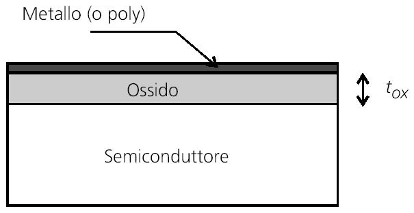
8 Oxidation 8
9 Photo-Lithographic Process 9
10 Etching 10
11 Patterning of SiO2 Si-substrate (a) Silicon base material Si-substrate (b) After oxidation and deposition of negative photoresist Si-substrate (c) Stepper exposure Photoresist SiO 2 UV-light Patterned optical mask Exposed resist Si-substrate Si-substrate Hardened resist SiO 2 (d) After development and etching of resist, chemical or plasma etch of SiO 2 Si-substrate (e) After etching Chemical or plasma etch Hardened resist SiO 2 SiO 2 (f) Final result after removal of resist 11
12 Ion Implantation 12
13 Metal Deposition 13
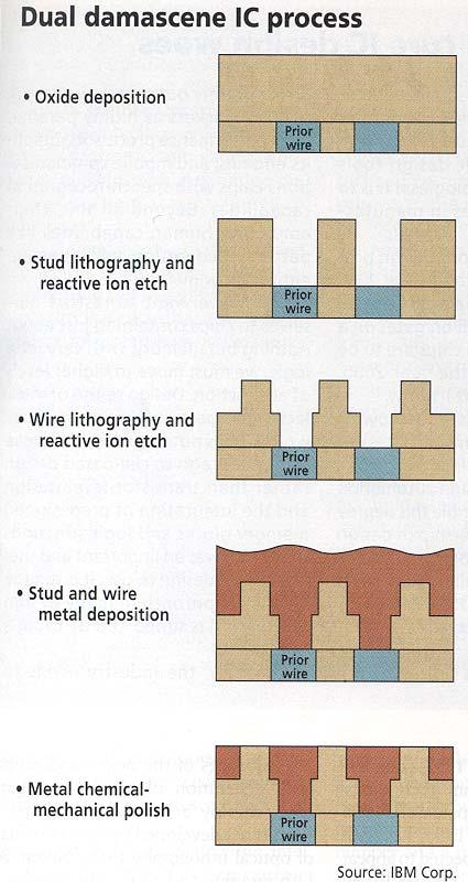
14 CMOS Process at a Glance Define active areas Etch and fill trenches Implant well regions Deposit and pattern polysilicon layer Implant source and drain regions and substrate contacts Create contact and via windows Deposit and pattern metal layers 14
15 CMOS Process Walk-Through p-epi p+ (a) Base material: p+ substrate with p-epi layer p-epi p+ SiN 3 4 SiO 2 (b) After deposition of gate-oxide and sacrificial nitride (acts as a buffer layer) p+ (c) After plasma etch of insulating trenches using the inverse of the active area mask 15
16 CMOS Process Walk-Through SiO 2 (d) After trench filling, CMP planarization, and removal of sacrificial nitride n (e) After n-well and V Tp adjust implants p (f) After p-well and V Tn adjust implants 16
17 CMOS Process Walk-Through poly(silicon) (g) After polysilicon deposition and etch n+ p+ (h) After n+ source/drain and p+source/drain implants. These steps also dope the polysilicon. SiO 2 (i) After deposition of SiO 2 insulator and contact hole etch. 17
18 CMOS Process Walk-Through Al (j) After deposition and patterning of first Al layer. Al SiO 2 (k) After deposition of SiO 2 insulator, etching of via s, deposition and patterning of second layer of Al. 18
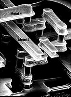
19 Advanced Metallization 19
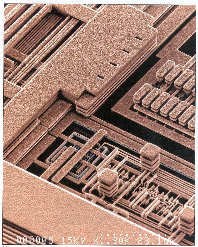
20 Advanced Metallization 20

21 3D Perspective Polysilicon Aluminum 21

22 Silicon-on on-insulator Process 22

23 BJT Process 23

24 BJT Process 24

25 BJT Process 25

26 Resistors 26
27 Capacitances 27
28 Design Rules 28
29 Design Rules Interface between designer and process engineer Guidelines for constructing process masks Unit dimension: Minimum line width scalable design rules: lambda parameter absolute dimensions (micron rules) 29

30 Layers in 0.25μm CMOS process 30
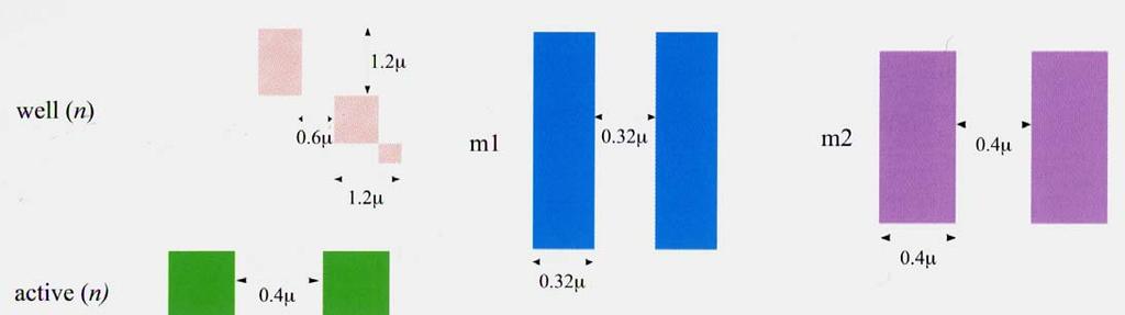
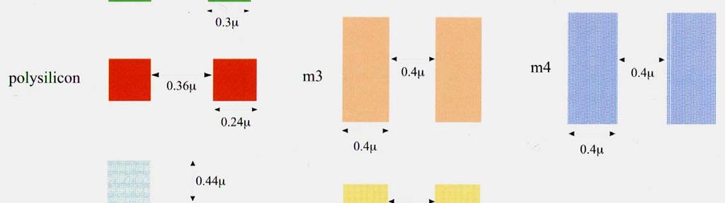
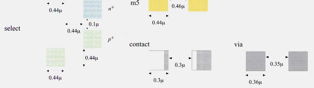
31 Intra-layer layout design rules 31

32 Transistor layout PMOS 32


33 Contacts and vias design rules 33

34 Well contacts and select layer design rules 34

35 Design Rule Checker poly_not_fet to all_diff minimum spacing = 0.14 um. 35

36 Latch-up CMOS structure with parasitic npn and pnp transistors identified 36
37 Latch-up V DD R nwell p-source n-source R psub CMOS latch-up: equivalent circuit 37
38 Circuit Under Design V DD V DD M2 M4 V in V out V out2 M1 M3 38

39 Layout of two chained CMOS inveters 39
40 CMOS Process Layers Layer Well (p,n) Active Area (n+,p+) Select (p+,n+) Polysilicon Metal1 Metal2 Contact To Poly Contact To Diffusion Via Color Yellow Green Green Red Blue Magenta Black Black Black Representation 40
41 CMOS Inverter Layout GND In V DD A A Out (a) Layout A A p-substrate n Field Oxide n + (b) Cross-Section along A-A p + 41

42 Four-input CMOS NAND layout 42
43 Computing the Capacitances 43
44 Parasitic Capacitances V DD V DD V in C gd12 M2 C db2 V out C g4 M4 V out2 M1 C db1 C w Interconnect C g3 M3 Fanout Simplified Model V in V out C L 44
 GND 45")
45 Layout of the Cascaded Inverter Pair PMOS (9λ/ 2λ) V DD 0.25 μm = 2λ In Out Metal1 Polysilicon NMOS (3λ/ 2λ) GND 45
46 Inverter Transistor Data 46
47 Components of C L 47
48 Capacitances Parameters in 0.25 μm CMOS process 48
49 The Overlape Capacitance Polysilicon gate Source n + x d x d W Drain n + L d Top view Gate-bulk overlap t ox Gate oxide n + L n + Cross section 49
50 The Miller Effect 50
51 Source Junction Channel-stop implant N A + Side wall W Source N D Bottom x j L S Side wall Substrate N A Channel 51
52 Junction Capacitance (1) 52
53 Junction Capacitance (2) 53
54 K for eq a 2.5 V CMOS Inverter 54
55 Gate-to to-channel Capacitance G G G S C GC C GC C GC D S D S D Cut-off Resistive Saturation 55
56 Wire Capacitance Tipycal interconnect capacitances for 0.25 μm CMOS process (wires routed over the field oxide): - Al1 area capacitance = 30 af/μm 2 - Poly area capacitance = 88 af/μm 2 From the layout: - poly area = 72 λ 2 - Al1 area = 42 λ 2 C W = 42 λ 2 30 af/μm λ 2 88 af/μm 2 = 0.12 ff 56
Manufacturing Process
 CMOS Manufacturing Process CMOS Process 1 A Modern CMOS Process gate-oxide TiSi AlCu Tungsten SiO n+ p-well p-epi poly n-well p+ SiO p+ Dual-Well Trench-Isolated CMOS Process Circuit Under Design V DD
CMOS Manufacturing Process
 CMOS Manufacturing Process CMOS Process A Modern CMOS Process gate-oxide TiSi 2 AlCu Tungsten SiO 2 n+ p-well p-epi poly n-well p+ SiO 2 p+ Dual-Well Trench-Isolated CMOS Process Circuit Under Design V
9/4/2008 GMU, ECE 680 Physical VLSI Design
 ECE680: Physical VLSI Design Chapter II CMOS Manufacturing Process 1 Dual-Well Trench-Isolated CMOS Process gate-oxide TiSi 2 AlCu Tungsten SiO 2 p-well poly n-well SiO 2 n+ p-epi p+ p+ 2 Schematic Layout
We are moving to 155 Donner Lab From Thursday, Feb 2 We will be able to accommodate everyone!
 -Spring 006 Digital Integrated Circuits Lecture 4 CMOS Manufacturing Process Design Rules EECS141 1 Good News! We are moving to 155 Donner Lab From Thursday, Feb We will be able to accommodate everyone!
Manufacturing Process
 Digital Integrated Circuits A Design Perspective Jan M. Rabaey Anantha Chandrakasan Borivoje Nikolic Manufacturing Process July 30, 2002 1 CMOS Process 2 A Modern CMOS Process gate-oxide TiSi 2 AlCu Tungsten
ECE 659. Jan M. Rabaey Anantha Chandrakasan Borivoje Nikolic. July 30, Digital EE141 Integrated Circuits 2nd Manufacturing.
 Digital Integrated Circuits A Design Perspective Jan M. Rabaey Anantha Chandrakasan Borivoje Nikolic Manufacturing Process July 0, 00 1 CMOS Process 1 A Modern CMOS Process gate-oxide TiSi AlCu Tungsten
Chapter 2 Manufacturing Process
 Digital Integrated Circuits A Design Perspective Chapter 2 Manufacturing Process 1 CMOS Process 2 CMOS Process (n-well) Both NMOS and PMOS must be built in the same silicon material. PMOS in n-well NMOS
CMOS Manufacturing process. Design rule set
 CMOS Manufacturing process Circuit design Set of optical masks Fabrication process Circuit designer Design rule set Process engineer All material: Chap. 2 of J. Rabaey, A. Chandrakasan, B. Nikolic, Digital
Cost of Integrated Circuits
 Cost of IC Design 1 Cost of Integrated Circuits NRE (Non-Recurrent Engineering) costs fixed design time and effort, mask generation independent of sales volume / number of products one-time cost factor
Lecture 1A: Manufacturing& Layout
 Introduction to CMOS VLSI Design Lecture 1A: Manufacturing& Layout David Harris Harvey Mudd College Spring 2004 Steven Levitan Fall 2008 1 The Manufacturing Process For a great tour through the IC manufacturing
CMOS Manufacturing process. Circuit designer. Design rule set. Process engineer. Set of optical masks. Fabrication process.
 CMOS Manufacturing process Circuit design Set of optical masks Fabrication process Circuit designer Design rule set Process engineer All material: Chap. 2 of J. Rabaey, A. Chandrakasan, B. Nikolic, Digital
FABRICATION of MOSFETs
 FABRICATION of MOSFETs CMOS fabrication sequence -p-type silicon substrate wafer -creation of n-well regions for pmos transistors, -impurity implantation into the substrate. -thick oxide is grown in the
ECE321 Electronics I
 ECE321 Electronics I Lecture 19: CMOS Fabrication Payman Zarkesh-Ha Office: ECE Bldg. 230B Office hours: Tuesday 2:00-3:00PM or by appointment E-mail: payman@ece.unm.edu Slide: 1 Miller Effect Interconnect
PROCESS FLOW AN INSIGHT INTO CMOS FABRICATION PROCESS
 Contents: VI Sem ECE 06EC63: Analog and Mixed Mode VLSI Design PROCESS FLOW AN INSIGHT INTO CMOS FABRICATION PROCESS 1. Introduction 2. CMOS Fabrication 3. Simplified View of Fabrication Process 3.1 Alternative
VLSI Design and Simulation
 VLSI Design and Simulation CMOS Processing Technology Topics CMOS Processing Technology Semiconductor Processing How do we make a transistor? Fabrication Process Wafer Processing Silicon single crystal
CMOS FABRICATION. n WELL PROCESS
 CMOS FABRICATION n WELL PROCESS Step 1: Si Substrate Start with p- type substrate p substrate Step 2: Oxidation Exposing to high-purity oxygen and hydrogen at approx. 1000 o C in oxidation furnace SiO
ECE520 VLSI Design. Lecture 7: CMOS Manufacturing Process. Payman Zarkesh-Ha
 ECE520 VLSI Design Lecture 7: CMOS Manufacturing Process Payman Zarkesh-Ha Office: ECE Bldg. 230B Office hours: Wednesday 2:00-3:00PM or by appointment E-mail: pzarkesh@unm.edu Slide: 1 Review of Last
Department of Electrical Engineering. Jungli, Taiwan
 Chapter 3 Fabrication of CMOS Integrated Circuits Jin-Fu Li Department of Electrical Engineering National Central University Jungli, Taiwan Background Outline The CMOS Process Flow Design Rules Latchup
CMOS Technology. Flow varies with process types & company. Start with substrate selection. N-Well CMOS Twin-Well CMOS STI
 CMOS Technology Flow varies with process types & company N-Well CMOS Twin-Well CMOS STI Start with substrate selection Type: n or p Doping level, resistivity Orientation, 100, or 101, etc Other parameters
UT Austin, ECE Department VLSI Design 2. CMOS Fabrication, Layout Rules
 2. CMOS Fabrication, Layout, Design Rules Last module: Introduction to the course How a transistor works CMOS transistors This module: CMOS Fabrication Design Rules CMOS Fabrication CMOS transistors are
VLSI PROCESS TECHNOLOGY By ER. HIMANSHU SHARMA
 VLSI PROCESS TECHNOLOGY y ER. HIMNSHU SHRM Fabrication Masks Chips Wafers Processing Processed Wafer Traditional CMOS Process Modern CMOS Process Dual-Well Trench-Isolated CMOS gate oxide field oxide l
EEC 118 Lecture #5: MOS Fabrication. Rajeevan Amirtharajah University of California, Davis Jeff Parkhurst Intel Corporation
 EEC 118 Lecture #5: MOS Fabrication Rajeevan Amirtharajah University of California, Davis Jeff Parkhurst Intel Corporation Announcements Lab 3 this week, report due next week HW 3 due this Friday at 4
CS/ECE 5710/6710. N-type Transistor. N-type from the top. Diffusion Mask. Polysilicon Mask. CMOS Processing
 CS/ECE 5710/6710 CMOS Processing Addison-Wesley N-type Transistor D G +Vgs + Vds S N-type from the top i electrons - Diffusion Mask Mask for just the diffused regions Top view shows patterns that make
Chapter 3 CMOS processing technology
 Chapter 3 CMOS processing technology (How to make a CMOS?) Si + impurity acceptors(p-type) donors (n-type) p-type + n-type => pn junction (I-V) 3.1.1 (Wafer) Wafer = A disk of silicon (0.25 mm - 1 mm thick),
FABRICATION OF CMOS INTEGRATED CIRCUITS. Dr. Mohammed M. Farag
 FABRICATION OF CMOS INTEGRATED CIRCUITS Dr. Mohammed M. Farag Outline Overview of CMOS Fabrication Processes The CMOS Fabrication Process Flow Design Rules EE 432 VLSI Modeling and Design 2 CMOS Fabrication
Fabrication and Layout
 ECEN454 Digital Integrated Circuit Design Fabrication and Layout ECEN 454 3.1 A Glimpse at MOS Device Polysilicon Aluminum ECEN 475 4.2 1 Material Classification Insulators Glass, diamond, silicon oxide
CHAPTER - 4 CMOS PROCESSING TECHNOLOGY
 CHAPTER - 4 CMOS PROCESSING TECHNOLOGY Samir kamal Spring 2018 4.1 CHAPTER OBJECTIVES 1. Introduce the CMOS designer to the technology that is responsible for the semiconductor devices that might be designed
Introduction to CMOS VLSI Design. Layout, Fabrication, and Elementary Logic Design
 Introduction to CMOS VLSI Design Layout, Fabrication, and Elementary Logic Design CMOS Fabrication CMOS transistors are fabricated on silicon wafer Lithography process similar to printing press On each
VLSI INTRODUCTION P.VIDYA SAGAR ( ASSOCIATE PROFESSOR) Department of Electronics and Communication Engineering, VBIT
 Department of Electronics and Communication Engineering, VBIT") VLSI INTRODUCTION P.VIDYA SAGAR ( ASSOCIATE PROFESSOR) contents UNIT I INTRODUCTION: Introduction to IC Technology MOS, PMOS, NMOS, CMOS & BiCMOS technologies. BASIC ELECTRICAL PROPERTIES : Basic Electrical
VLSI INTRODUCTION P.VIDYA SAGAR ( ASSOCIATE PROFESSOR) contents UNIT I INTRODUCTION: Introduction to IC Technology MOS, PMOS, NMOS, CMOS & BiCMOS technologies. BASIC ELECTRICAL PROPERTIES : Basic Electrical
EE 143 FINAL EXAM NAME C. Nguyen May 10, Signature:
 INSTRUCTIONS Read all of the instructions and all of the questions before beginning the exam. There are 5 problems on this Final Exam, totaling 143 points. The tentative credit for each part is given to
EE 560 FABRICATION OF MOS CIRCUITS. Kenneth R. Laker, University of Pennsylvania
 1 EE 560 FABRICATION OF MOS CIRCUITS 2 CMOS CHIP MANUFACTRING STEPS Substrate Wafer Wafer Fabrication (diffusion, oxidation, photomasking, ion implantation, thin film deposition, etc.) Finished Wafer Wafer
Lecture 0: Introduction
 Lecture 0: Introduction Introduction Integrated circuits: many transistors on one chip. Very Large Scale Integration (VLSI): bucketloads! Complementary Metal Oxide Semiconductor Fast, cheap, low power
EE 330 Lecture 9. IC Fabrication Technology Part II. -Oxidation -Epitaxy -Polysilicon -Planarization -Resistance and Capacitance in Interconnects
 EE 330 Lecture 9 IC Fabrication Technology Part II -Oxidation -Epitaxy -Polysilicon -Planarization -Resistance and Capacitance in Interconnects Review from Last Time Etching Dry etch (anisotropic) SiO
EE 330 Lecture 9. IC Fabrication Technology Part II. -Oxidation -Epitaxy -Polysilicon -Planarization -Resistance and Capacitance in Interconnects
 EE 330 Lecture 9 IC Fabrication Technology Part II -Oxidation -Epitaxy -Polysilicon -Planarization -Resistance and Capacitance in Interconnects Review from Last Time IC Fabrication Technology Crystal Preparation
CMOS Processing Technology
 CHAPTER 2 CMOS Processing Technology Outline 2 1. CMOS Technologies 2. Layout Design Rules 3. CMOS Process Enhancements 4. Technology-related CAD Issues 5. Manufacturing Issues CMOS Technologies 3 n-well
CMOS Processing Technology
 CHAPTER 2 CMOS Processing Technology Outline 2 1. CMOS Technologies 2. Layout Design Rules 3. CMOS Process Enhancements 4. Technology-related CAD Issues 5. Manufacturing Issues CMOS Technologies 3 n-well
CMOS Fabrication. Dr. Bassam Jamil. Adopted from slides of the textbook
 CMOS Fabrication Dr. Bassam Jamil Adopted from slides of the textbook CMOS Fabrication CMOS transistors are fabricated on silicon wafer Lithography process similar to printing press On each step, different
Fabrication and Layout
 Fabrication and Layout Kenneth Yun UC San Diego Adapted from EE271 notes, Stanford University Overview Semiconductor properties How chips are made Design rules for layout Reading Fabrication: W&E 3.1,
EE40 Lec 22. IC Fabrication Technology. Prof. Nathan Cheung 11/19/2009
 Suggested Reading EE40 Lec 22 IC Fabrication Technology Prof. Nathan Cheung 11/19/2009 300mm Fab Tour http://www-03.ibm.com/technology/manufacturing/technology_tour_300mm_foundry.html Overview of IC Technology
Integrated Circuits & Systems
 Federal University of Santa Catarina Center for Technology Computer Science & Electronics Engineering Integrated Circuits & Systems INE 5442 Lecture 6 CMOS Fabrication Process & Design Rules guntzel@inf.ufsc.br
CMOS VLSI Design. Introduction. All materials are from the textbook Weste and Harris, 3 rd Edition CMOS VLSI DESIGN. Introduction
 CMOS VLSI Design Introduction ll materials are from the textbook Weste and Harris, 3 rd Edition CMOS VLSI DESIGN Introduction Chapter previews the entire field, subsequent chapters elaborate on specific
Lecture 030 Integrated Circuit Technology - I (5/8/03) Page 030-1
 Page 030-1") Lecture 030 Integrated Circuit Technology - I (5/8/03) Page 030-1 LECTURE 030 INTEGRATED CIRCUIT TECHNOLOGY - I (References [7,8]) Objective The objective of this presentation is: 1.) Illustrate integrated
Lecture 030 Integrated Circuit Technology - I (5/8/03) Page 030-1 LECTURE 030 INTEGRATED CIRCUIT TECHNOLOGY - I (References [7,8]) Objective The objective of this presentation is: 1.) Illustrate integrated
EE 330 Lecture 9. IC Fabrication Technology Part 2
 EE 330 Lecture 9 IC Fabrication Technology Part 2 Quiz 8 A 2m silicon crystal is cut into wafers using a wire saw. If the wire diameter is 220um and the wafer thickness is 350um, how many wafers will this
EE 434 Lecture 9. IC Fabrication Technology
 EE 434 Lecture 9 IC Fabrication Technology Quiz 7 The layout of a film resistor with electrodes A and B is shown. If the sheet resistance of the film is 40 /, determine the resistance between nodes A and
Czochralski Crystal Growth
 Czochralski Crystal Growth Crystal Pulling Crystal Ingots Shaping and Polishing 300 mm wafer 1 2 Advantage of larger diameter wafers Wafer area larger Chip area larger 3 4 Large-Diameter Wafer Handling
IC Fabrication Technology Part III Devices in Semiconductor Processes
 EE 330 Lecture 10 IC Fabrication Technology Part III Metalization and Interconnects Parasitic Capacitances Back-end Processes Devices in Semiconductor Processes Resistors Diodes Review from Last Lecture
VLSI. Lecture 1. Jaeyong Chung System-on-Chips (SoC) Laboratory Incheon National University. Based on slides of David Money Harris
 Laboratory Incheon National University. Based on slides of David Money Harris") VLSI Lecture 1 Jaeyong Chung System-on-Chips (SoC) Laboratory Incheon National University Based on slides of David Money Harris Goals of This Course Learn the principles of VLSI design Learn to design
VLSI Lecture 1 Jaeyong Chung System-on-Chips (SoC) Laboratory Incheon National University Based on slides of David Money Harris Goals of This Course Learn the principles of VLSI design Learn to design
Isolation Technology. Dr. Lynn Fuller
 ROCHESTER INSTITUTE OF TECHNOLOGY MICROELECTRONIC ENGINEERING Isolation Technology Dr. Lynn Fuller Motorola Professor 82 Lomb Memorial Drive Rochester, NY 14623-5604 Tel (585) 475-2035 Fax (585) 475-5041
Lecture #18 Fabrication OUTLINE
 Transistors on a Chip Lecture #18 Fabrication OUTLINE IC Fabrication Technology Introduction the task at hand Doping Oxidation Thin-film deposition Lithography Etch Lithography trends Plasma processing
VLSI Systems and Computer Architecture Lab
 ΚΥΚΛΩΜΑΤΑ VLSI Πανεπιστήμιο Ιωαννίνων CMOS Technology Τμήμα Μηχανικών Η/Υ και Πληροφορικής 1 From the book: An Introduction ti to VLSI Process By: W. Maly ΚΥΚΛΩΜΑΤΑ VLSI Διάρθρωση 1. N well CMOS 2. Active
Silicon Wafer Processing PAKAGING AND TEST
 Silicon Wafer Processing PAKAGING AND TEST Parametrical test using test structures regularly distributed in the wafer Wafer die test marking defective dies dies separation die fixing (not marked as defective)
Process Integration. MEMS Release Techniques Sacrificial Layer Removal Substrate Undercut
 Process Integration Self-aligned Techniques LOCOS- self-aligned channel stop Self-aligned Source/Drain Lightly Doped Drain (LDD) Self-aligned silicide (SALICIDE) Self-aligned oxide gap MEMS Release Techniques
Exam 1 Friday Sept 22
 Exam 1 Friday Sept 22 Students may bring 1 page of notes Next weeks HW assignment due on Wed Sept 20 at beginning of class No 5:00 p.m extension so solutions can be posted Those with special accommodation
Microfabrication of Integrated Circuits
 Microfabrication of Integrated Circuits OUTLINE History Basic Processes Implant; Oxidation; Photolithography; Masks Layout and Process Flow Device Cross Section Evolution Lecture 38, 12/05/05 Reading This
Process Integration. NMOS Generic NMOS Process Flow. CMOS - The MOSIS Process Flow
 Process Integration Self-aligned Techniques LOCOS- self-aligned channel stop Self-aligned Source/Drain Lightly Doped Drain (LDD) Self-aligned silicide (SALICIDE) Self-aligned oxide gap MEMS Release Techniques
VLSI Digital Systems Design
 VLSI Digital Systems Design CMOS Processing cmpe222_03process_ppt.ppt 1 Si Purification Chemical purification of Si Zone refined Induction furnace Si ingot melted in localized zone Molten zone moved from
MOS Front-End. Field effect transistor
 MOS Front-End Back-end Transistor Contact Front-end p-well STI n-well Front-end-of-line includes substrate, isolation, wells, transistor, silicide Field effect transistor MOSFET: Metal-Oxide-Semiconductor
ASIC Physical Design CMOS Processes
 ASIC Physical Design CMOS Processes Smith Text: Chapters 2 & 3 Weste CMOS VLSI Design Global Foundries: BiCMOS_8HP8XP_Training.pdf BiCMOS_8HP_Design_Manual.pdf Physical design process overview CMOS transistor
Lecture 19 Microfabrication 4/1/03 Prof. Andy Neureuther
 EECS 40 Spring 2003 Lecture 19 Microfabrication 4/1/03 Prof. ndy Neureuther How are Integrated Circuits made? Silicon wafers Oxide formation by growth or deposition Other films Pattern transfer by lithography
Lecture 2: CMOS Fabrication Mark McDermott Electrical and Computer Engineering The University of Texas at Austin
 Lecture 2: CMOS Fabrication Mark McDermott Electrical and Computer Engineering The University of Texas at Austin Agenda Last module: Introduction to the course How a transistor works CMOS transistors This
Complexity of IC Metallization. Early 21 st Century IC Technology
 EECS 42 Introduction to Digital Electronics Lecture # 25 Microfabrication Handout of This Lecture. Today: how are Integrated Circuits made? Silicon wafers Oxide formation by growth or deposition Other
EE 330 Lecture 8. IC Fabrication Technology Part II. - Oxidation - Epitaxy - Polysilicon - Interconnects
 EE 330 Lecture 8 IC Fabrication Technology Part II - Oxidation - Epitaxy - Polysilicon - Interconnects Review from Last Time MOS Transistor Bulk Source Gate Drain p-channel MOSFET Lightly-doped n-type
EE CMOS TECHNOLOGY- Chapter 2 in the Text
 1 EE 212 FALL 1999-00 CMOS TECHOLOGY- Chapter 2 in the Text In this set of notes we will describe a modern CMOS process flow. In the simplest CMOS technologies, we need to realize simply MOS and MOS transistors
Lecture 200 BiCMOS Technology (12/12/01) Page 200-1
 Page 200-1") Lecture 200 BiCMOS Technology (12/12/01) Page 200-1 LECTURE 200 BICMOS TECHNOLOGY (READING: Text-Sec. 2.11) INTRODUCTION Objective Illustrate BiCMOS technology Outline Introduction Physical process illustration
Lecture 200 BiCMOS Technology (12/12/01) Page 200-1 LECTURE 200 BICMOS TECHNOLOGY (READING: Text-Sec. 2.11) INTRODUCTION Objective Illustrate BiCMOS technology Outline Introduction Physical process illustration
conductor - gate insulator source gate n substrate conductor - gate insulator gate substrate n open switch closed switch however: closed however:
 MOS Transistors Readings: Chapter 1 N-type drain conductor - gate insulator source gate drain source n p n substrate P-type drain conductor - gate insulator source drain gate source p p substrate n 42
HOMEWORK 4 and 5. March 15, Homework is due on Monday March 30, 2009 in Class. Answer the following questions from the Course Textbook:
 HOMEWORK 4 and 5 March 15, 2009 Homework is due on Monday March 30, 2009 in Class. Chapter 7 Answer the following questions from the Course Textbook: 7.2, 7.3, 7.4, 7.5, 7.6*, 7.7, 7.9*, 7.10*, 7.16, 7.17*,
Semiconductor Manufacturing Technology. IC Fabrication Process Overview
 Semiconductor Manufacturing Technology Michael Quirk & Julian Serda October 00 by Prentice Hall Chapter 9 IC Fabrication Process Overview /4 Objectives After studying the material in this chapter, you
Low Power VLSI Circuits and Systems Prof. Ajit Pal Department of Computer Science and Engineering Indian Institute of Technology, Kharagpur
 Low Power VLSI Circuits and Systems Prof. Ajit Pal Department of Computer Science and Engineering Indian Institute of Technology, Kharagpur Lecture No. # 02 MOS Transistors - I Hello and welcome to today
Fairchild Semiconductor Application Note June 1983 Revised March 2003
 Fairchild Semiconductor Application Note June 1983 Revised March 2003 High-Speed CMOS (MM74HC) Processing The MM74HC logic family achieves its high speed by utilizing microcmos Technology. This is a 3.5
EE 330 Lecture 8. IC Fabrication Technology Part II. - Masking - Photolithography - Deposition - Etching - Diffusion
 EE 330 Lecture 8 IC Fabrication Technology Part II?? - Masking - Photolithography - Deposition - Etching - Diffusion Review from Last Time Technology Files Provide Information About Process Process Flow
Complementary Metal-Oxide-Semiconductor Very Large-Scale Integrated Circuit Design
 Complementary Metal-Oxide-Semiconductor Very Large-Scale Integrated Circuit Design Bradley A. Minch Mixed Analog-Digital VLSI Circuits and Systems Lab Cornell University Ithaca, NY 14853 5401 minch@ece.cornell.edu
Chapter 2 Problems. The CMOS technology we need to realize is shown below, from Figure 1-34 in the text. S P + N P + N WELL P +
 Chapter 2 roblems 2.1 Sketch a process flow that would result in the structure shown in Figure 1-34 by drawing a series of drawings similar to those in this chapter. You only need to describe the flow
INTEGRATED-CIRCUIT TECHNOLOGY
 INTEGRATED-CIRCUIT TECHNOLOGY 0. Silicon crystal growth and wafer preparation 1. Processing Steps 1.1. Photolitography 1.2. Oxidation 1.3. Layer Deposition 1.4. Etching 1.5. Diffusion 1.6 Backend: assembly,
This Appendix discusses the main IC fabrication processes.
 IC Fabrication B B.1 Introduction This Appendix discusses the main IC fabrication processes. B.2 NMOS fabrication NMOS transistors are formed in a p-type substrate. The NMOS fabrication process requires
Lecture 2. Fabrication and Layout
 Lecture 2 Fabrication and Layout Mark Horowitz Modified by Azita Emami Computer Systems Laboratory Stanford University azita@stanford.edu 1 Overview Reading W&E 3.1(scan), 3.2.1, 3.3.1 - Fabrication W&E
THE MANUFACTURING PROCESS
 chapter2.fm Page 33 Monday, September 4, 2000 11:11 AM CHAPTER 2 THE MANUFACTURING PROCESS Overview of manufacturing process n Design rules n IC packaging n Future Trends in Integrated Circuit Technology
Chapter 4 : ULSI Process Integration (0.18 m CMOS Process)
") Chapter : ULSI Process Integration (0.8 m CMOS Process) Reference. Semiconductor Manufacturing Technology : Michael Quirk and Julian Serda (00). - (00). Semiconductor Physics and Devices- Basic Principles(/e)
Chapter : ULSI Process Integration (0.8 m CMOS Process) Reference. Semiconductor Manufacturing Technology : Michael Quirk and Julian Serda (00). - (00). Semiconductor Physics and Devices- Basic Principles(/e)
Isolation of elements
 1 In an IC, devices on the same substrate must be isolated from one another so that there is no current conduction between them. Isolation uses either the junction or dielectric technique or a combination
Microelectronics. Integrated circuits. Introduction to the IC technology M.Rencz 11 September, Expected decrease in line width
 Microelectronics Introduction to the IC technology M.Rencz 11 September, 2002 9/16/02 1/37 Integrated circuits Development is controlled by the roadmaps. Self-fulfilling predictions for the tendencies
Schematic creation of MOS field effect transistor.
 Schematic creation of MOS field effect transistor. Gate electrode Drain electrode Source electrode Gate oxide Gate length Page 1 Step 0 The positively doped silicon wafer is first coated with an insulating
National Semiconductor LM2672 Simple Switcher Voltage Regulator
 Construction Analysis National Semiconductor LM2672 Simple Switcher Voltage Regulator Report Number: SCA 9712-570 Global Semiconductor Industry the Serving Since 1964 17350 N. Hartford Drive Scottsdale,
VLSI Technology Dr. Nandita Dasgupta Department of Electrical Engineering Indian Institute of Technology, Madras
 VLSI Technology Dr. Nandita Dasgupta Department of Electrical Engineering Indian Institute of Technology, Madras Lecture - 36 MOSFET I Metal gate vs self-aligned poly gate So far, we have discussed about
Historical Development. Babbage s second computer. Before the digital age
 Historical Development To fully appreciate the computers of today, it is helpful to understand how things got the way they are The evolution of computing machinery has taken place over several centuries
UNIT 4. By: Ajay Kumar Gautam Asst. Prof. Dev Bhoomi Institute of Technology & Engineering, Dehradun
 UNIT 4 By: Ajay Kumar Gautam Asst. Prof. Dev Bhoomi Institute of Technology & Engineering, Dehradun Syllabus METALLIZATION: Applications and choices, physical vapor deposition, patterning, problem areas.
Chapter 2 MOS Fabrication Technology
 Chapter 2 MOS Fabrication Technology Abstract This chapter is concerned with the fabrication of metal oxide semiconductor (MOS) technology. Various processes such as wafer fabrication, oxidation, mask
Microelettronica. Planar Technology for Silicon Integrated Circuits Fabrication. 26/02/2017 A. Neviani - Microelettronica
 Microelettronica Planar Technology for Silicon Integrated Circuits Fabrication 26/02/2017 A. Neviani - Microelettronica Introduction Simplified crosssection of an nmosfet and a pmosfet Simplified crosssection
EE 143 CMOS Process Flow
 EE 143 CMOS rocess Flow CT 84 D D G Sub G Sub S S G D S G D S + + + + - MOS Substrate Well - MOS Substrate EE 143 CMOS rocess Flow CT 85 hotoresist Si 3 4 SiO 2 Substrate selection: moderately high resistivity,
Figure 2.3 (cont., p. 60) (e) Block diagram of Pentium 4 processor with 42 million transistors (2000). [Courtesy Intel Corporation.
 (e) Block diagram of Pentium 4 processor with 42 million transistors (2000). [Courtesy Intel Corporation.") Figure 2.1 (p. 58) Basic fabrication steps in the silicon planar process: (a) oxide formation, (b) selective oxide removal, (c) deposition of dopant atoms on wafer, (d) diffusion of dopant atoms into exposed
Figure 2.1 (p. 58) Basic fabrication steps in the silicon planar process: (a) oxide formation, (b) selective oxide removal, (c) deposition of dopant atoms on wafer, (d) diffusion of dopant atoms into exposed
Lect. 2: Basics of Si Technology
 Unit processes Thin Film Deposition Etching Ion Implantation Photolithography Chemical Mechanical Polishing 1. Thin Film Deposition Layer of materials ranging from fractions of nanometer to several micro-meters
Problem 1 Lab Questions ( 20 points total)
") Problem 1 Lab Questions ( 20 points total) (a) (3 points ) In our EE143 lab, we use Phosphorus for the source and drain diffusion. However, most advanced processes use Arsenic. What is the advantage of
Problem 1 Lab Questions ( 20 points total) (a) (3 points ) In our EE143 lab, we use Phosphorus for the source and drain diffusion. However, most advanced processes use Arsenic. What is the advantage of
Analog Devices ADSP KS-160 SHARC Digital Signal Processor
 Construction Analysis Analog Devices ADSP-21062-KS-160 SHARC Digital Signal Processor Report Number: SCA 9712-575 Global Semiconductor Industry the Serving Since 1964 17350 N. Hartford Drive Scottsdale,
Complementary Metal Oxide Semiconductor (CMOS)
") Technische Universität Graz Institute of Solid State Physics Complementary Metal Oxide Semiconductor (CMOS) Franssila: Chapters 26,28 Technische Universität Graz Institute of Solid State Physics Complementary
Technische Universität Graz Institute of Solid State Physics Complementary Metal Oxide Semiconductor (CMOS) Franssila: Chapters 26,28 Technische Universität Graz Institute of Solid State Physics Complementary
VLSI Technology Dr. Nandita Dasgupta Department of Electrical Engineering Indian Institute of Technology, Madras
 VLSI Technology Dr. Nandita Dasgupta Department of Electrical Engineering Indian Institute of Technology, Madras Lecture - 32 IC BJT - From junction isolation to LOCOS So, by now, we have completed all
Lecture 7 CMOS MEMS. CMOS MEMS Processes. CMOS MEMS Processes. Why CMOS-MEMS? Agenda: CMOS MEMS: Fabrication. MEMS structures can be made
 EEL6935 Advanced MEMS (Spring 2005) Instructor: Dr. Huikai Xie CMOS MEMS Agenda: Lecture 7 CMOS MEMS: Fabrication Pre-CMOS Intra-CMOS Post-CMOS Deposition Etching Why CMOS-MEMS? Smart on-chip CMOS circuitry
Lecture 22: Integrated circuit fabrication
 Lecture 22: Integrated circuit fabrication Contents 1 Introduction 1 2 Layering 4 3 Patterning 7 4 Doping 8 4.1 Thermal diffusion......................... 10 4.2 Ion implantation.........................
Micron Semiconductor MT5C64K16A1DJ 64K x 16 SRAM
 Construction Analysis Micron Semiconductor MT5C64K16A1DJ 64K x 16 SRAM Report Number: SCA 9412-394 Global Semiconductor Industry the Serving Since 1964 17350 N. Hartford Drive Scottsdale, AZ 85255 Phone:
Intel Pentium Processor W/MMX
 Construction Analysis Intel Pentium Processor W/MMX Report Number: SCA 9706-540 Global Semiconductor Industry the Serving Since 1964 15022 N. 75th Street Scottsdale, AZ 85260-2476 Phone: 602-998-9780 Fax:
Mosel Vitelic MS62256CLL-70PC 256Kbit SRAM
 Construction Analysis Mosel Vitelic MS62256CLL-70PC 256Kbit SRAM Report Number: SCA 9703-499 Global Semiconductor Industry the Serving Since 1964 17350 N. Hartford Drive Scottsdale, AZ 85255 Phone: 602-515-9780