CHAPTER 4: MOST PROCESSING TECHNOLOGY
|
|
|
- Henry Hardy
- 6 years ago
- Views:
Transcription
1 CHAPTER 4: MOST PROCESSING TECHNOLOGY
2 Introduction Objectives: 1. Discuss the fundamentals of MOST chip fabrication and examined the major steps of the process flow 2. Emphasis only on the general outline of process flow and the interaction of various processing steps, which ultimately determine the device & circuit performance 3. To show that there are very strong links between the fabrication process, circuit design process and the performance of the resulting chip 4. Start with an introduction to semiconductor manufacturing process, then to NMOS processing flow and finally to CMOS fabrication steps 5. Later the Layout design rules will be cover
3 Silicon Semiconductor Manufacturing Technology Overview Semiconductor? Silicon or Germanium Why called as semiconductor? Conductivity between conductor & insulator How to change this conductivity? Introducing impurity atoms or dopants 2 type of dopants? Electron or Holes Impurity use electron = acceptors else donors Si contains majority of donors = n-type else p-type When p & n-type brought together = junction = diode When make 2 junction = pnp or npn = bipolar When make metal-oxide-semiconductor = MOST
4 Wafer processing Wafer is a disk of Silicon varies from 75mm to 230mm and less than 1mm thick Wafer are cut from ingots of singlecrystal silicon that been pulled from crucible melt of pure molten polycrystalline silicon
5 Oxidation Process to make SiO 2 Achieved by heating Si wafers in an oxidizing atmosphere such as oxygen or water vapor 2 common approaches: 1. Wet Oxidation : When oxidizing atmosphere is water vapor with temperature between 900 C & 1000 C that rapidly process 2. Dry Oxidation : When oxidizing atmosphere is purely oxygen with temperature in range of 1200 C The oxidation process consumes silicon
6 Epitaxy, Deposition, Ion-Implantation Implantation & Diffusion, Etching Epitaxy growing a thin single-crystal film on silicon surface by subjecting the surface to elevated temperature and a source of dopant material Deposition Evaporating dopant material onto the silicon surface followed by a thermal cycle, which is used to drive the impurities from surface of silicon into the bulk Ion-Implantation Subjecting the silicon substrate to highly energized donor or acceptor atom that makes the atom travel below the surface, forming regions with varying doping concentrations Diffusion Occur at temperature > 800 C between any silicon that has differing densities of impurities, with impurities tend to diffuse from areas of high concentration to low Etching Removing unwanted layers on silicon surfaces either using wet or dry etching depending on required pattern
7 Basic Steps of Fabrication Process Flow Construction of transistors depends on the ability to control where & how many & what type of impurities are introduced into silicon wafer What Material of impurities/dopant source: 1. Boron for acceptor silicon (p-type) 2. Arsenic / Phosphorus donor (n-type) How much? Determined by the energy (in ev) & time of ionimplantation or the time & temperature of deposition & diffusion steps Where it used determine by using special materials called as masks In places covered by mask, the ion-implantation does not occur else it will occur 4 type of material commonly used for masking: 1. Photoresist 2. Polysilicon 3. Silicon dioxide (SiO 2 ) 4. Silicon nitride (SiN) Thus, we could say that the basic of fabrication process steps requires that certain area are defined on wafer / chip by appropriate masks that can be viewed as creating a different layer for different material
8 Continued In general, a layer must be patterned before next layer of material is applied on chip Photolithography is the process used to transfer a pattern to a layer on the chip that must be repeated for each layer since it has its own distinct patterning requirement by using different masks Thus, masking process involve: 1. Patterning windows in a mask material on the surface of wafer 2. Subjecting exposed areas to a dopant source 3. Removing any unwanted mask material
9 SiO 2 Patterning UV-light Si - substrate 1. Silicon Wafer Glass mask with feature Insoluble photoresist Oxide Si - substrate 2. Create oxide layer on Si Surface Oxide Si - substrate Expose photoresist becomes soluble Photoresist Oxide Si - substrate 3. Deposition of photoresist layer on top of oxide, which is essentially lightsensitive, acid-resistant organic polymer & initially insoluble 4. If photoresist exposed to UV light, exposed areas becomes soluble so that the region are no longer resistant to etching solvents. It is done by selectively covered the opaque features on the glass mask. Positive photoresist initially insoluble and becomes soluble when expose to UV Negative photoresist initially soluble and becomes insoluble when expose to UV
10 Continued Chemical etch (HF acid) or dry etch (plasma) Hardened photoresist window Oxide Oxide Oxide Si - substrate Si - substrate Si - substrate 5. Etched away oxide regions not covered by hardened photoresist using either Chemical etch (HF acid) or dry etch (plasma) process 6. End of etch process will obtain oxide window that reaches down to the silicon surfaces 7. Stripped out the remaining photoresist from oxide surface using another solvent, leaving the patterned oxide feature on the surface of silicon
11 Note: Previous sequence of process only for a single pattern transfer onto oxide surface, the fabrication of semiconductor devices requires several such pattern transfers to be performed on silicon dioxide, polysilicon & metal However, the basic of patterning process used in fabrication process is quite similar to discuss oxide patterning For accurate generation of high density patterns required in sub-micron devices, electron beam (E-beam) lithography is used instead of optical lithography
12 Fabrication of the MOS transistor Si - substrate Oxide Si - substrate 1. Silicon Wafer 2. Create oxide layer on Si Surface - Oxidation Thin Oxide Polysi SiO 2 SiO 2 Si - substrate Polysi Thin Oxide 5. Deposit polysi that used for both as gate electrode & interconnect medium in Si Chip. PolySi has high resistivity & reduce by doping it with impurity atom SiO 2 SiO 2 Si - substrate 3. SiO 2 patterning Selectively etched oxide to expose Si surface on which MOST will be created SiO 2 SiO 2 Si - substrate Polysi 6. Patterned & etched polysi to form interconnects & MOST gates Thin Oxide 4. Deposit a thin, highquality oxide layer SiO 2 SiO 2 on surface which will Si - substrate be the gate oxide of MOST SiO 2 SiO 2 Si - substrate 7. Etched away thin & single oxide not cover by PolySi, which exposed bare Si Surface on which source & drain junctions are to be formed
13 Continued Donor atoms impurity polysi SiO 2 SiO 2 n+ n+ Si - substrate 8. Doped the entire si surface with high conc. Of impurities by an ion implantation (donor n-type or acceptor p-type). We see that doping impurities penetrates the exposed areas on si surface, ultimately creating 2 n-type regions for source & drain in the p-type substrate. Also it penetrates the polysi on surface & reduce it resistivity. Note that polysi gate that patterned before doping actually define the precise location of channel region and hence the source & drain regions. This called as self-aligned process since it allows a very precise positioning of the 2 regions relative to gate. Insulating oxide polysi SiO 2 SiO 2 n+ n+ 9. Entire si surface is again covered by an insulating oxide and then patterned to provide a contact windows for drain & source junctions. Si - substrate polysi SiO 2 SiO 2 n+ n+ Si - substrate 10. Entire si surface is covered with evaporated aluminium which will form the interconnects and finally patterned & etched completing the interconnection of the MOST on the surfaces.
14 Device Isolation Techniques MOST that comprises of IC must be electrically isolated from each other during fabrication Isolation important for: 1. Preventing unwanted conductions paths between devices 2. Avoiding creation of inversion layers outside channel region of transistors 3. Reducing leakage currents How? The devices are typically created in dedicated regions called active areas, where each active areas is surrounded by a relatively thick oxide barrier called field oxide One method has discuss previously, where a thick field oxide grow on entire of Si surface and then selectively etch oxide in certain regions, to define active area. This method has some drawback: 1. Thickness of field oxide will leads to rather large oxide steps at boundaries b/w active areas & isolation regions 2. When polysi & metal layers are deposited over such boundaries in subsequent process, the sheer height differences at the boundary can cause cracking of deposited layers, leading to chip failure. To prevent it, most manufactures prefer a method that partially recess the field oxide into Si surface, resulting in more planar surface topology called LOCOS Local Oxidation of Silicon
15 LOCOS Technique based on selectively growing the field oxide in certain regions, instead of selectively etching away the active areas after oxide growth. Selectively oxide growth achieved by shielding active areas with Silicon Nitride (Si 3 N 4 ) during oxidation, which effectively inhibits oxide growth. Si 3 N 4 Pad oxide Si-Substrate Ion Implant Si 3 N 4 Si 3 N 4 p+ p+ p+ Si-Substrate Thick field oxide Si 3 N 4 Si 3 N 4 p+ p+ p+ Si-Substrate 1. Thin pad oxide grown on Si Surface, followed by deposition & patterning of Si 3 N 4 to mask/ define active area. 2. Thin pad oxide underneath Si 3 N 4 used to protect Si Surface from stress caused by nitride during an ion implantation of p- type to create channel-stop implants that surround the transistors. 3. Thick oxide is grown in area not covered by Si 3 N 4. Note that field oxide is partially recessed into surface since thermal oxidation also consumes Si. Also, the field oxide forms a lateral extension under nitride layer, called as bird beak that responsibly for reduction of active area. p+ Active area p+ p+ Si-Substrate Active area 4. Finally, nitride & thin pad oxide etch away resulting in active areas surrounded by partially recessed field oxide Note: 1. LOCOS is a popular method for achieving field oxide isolation with more planar surface topology 2. Several additional measures have also been developed over the years to control lateral bird beak encroachment, since it will ultimately limit the device scaling & density in VLSI circuits
16 LOCOS
17 Multilevel Interconnects and Metallization Multilevel Interconnects and Metallization Metal layers are needed for: 1. Creating interconnections between transistors 2. Routing power supply, signal & clock lines on chip surface Availability of multiple metal layers, where each are electrically isolated from neighboring layers by a dielectrics (SiO 2 ) allow: 1. Higher integration densities for realization of complex design 2. Adds third dimension that can be utilized very effectively in design The electrical connections between layers are made by vias that placed wherever such contact needed, that each via formed by: 1. Creating a window in isolation oxide before each new metallization step 2. Filling the opening oxide with special metal plug, usually tungsten to make via Following vias, the new layer of metal deposition & patterning will forms the next metallization level. Noted that the chip surface is highly nonplanar due to previous process steps to create the transistors, such as n-well or p-well creation, local oxidation & gate formation. Also it is not desirable to deposit multiple metal interconnects lines directly on this uneven surface topography since: 1. It may exhibit localized thinning & discontinuities at uneven surface edge 2. Photolithography is also difficult & imprecise 3. May eventually result in pronounced hills & valleys on the chip surface To avoid this problems of unplanar surface, the surface usually are planarized or flattened before each new metal deposition step by: 1. A fairly thick SiO 2 layer is deposited on surface to cover all existing surface ununiformities. 2. Then it planarized using several method such as glass reflow, etch-back or Chemical Mechanical Polishing (CMP) that used abrasive silica slurry is commonly adopted in industries.
18 Basic CMOS Technology Will discuss on n-well CMOS technologies, with a simplified treatment of process steps. This is necessary as it will be used as a guide for a better appreciation of the layout styles that used to implement CMOS gates. 4 main CMOS technologies: 1. n-well process 2. p-well process 3. Twin-tub process 4. Silicon on Insulator (SOI) During discussion of CMOS technologies, process cross sections and layouts will be presented. Fig. 3.6 summarizes the drawing conventions

19 Figure 3.6 CMOS process and layout drawing conventions
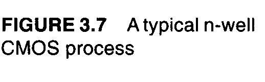
20 A Basic n-well Process 1. Creation of n-well: (fig. 3.7a) Moderately doped (impurity conc. Less than cm -3 ) p-type Si substrate Initial oxide layer grown on entire surface First lithographic mask (n-well mask) defines n-well region by an implanted of donor atoms, usually phosphorus into this window in oxide 2. Definition of Active areas & Field oxide (FOX) growth: Using LOCOS technique with p-type (Boron) implanted & n-well channel stop (resist) mask, fig 3.7b & c Stripped photoresist mask, leave the previously masked SiO 2 /SiN sandwich defining active areas, fig 3.7d Follow by growth thick Field Oxide (FOX) where SiN is absent, fig 3.7d 3. Polysilicon Deposition: (fig. 3.7e) Involves deposition of polysi into surface & then etching the required pattern (inverted U ) after completed previous steps of LOCOS 4. Source/Drain region Implantation: By using n+ mask, the thin-oxide & polysi areas implanted by n-type ion that will create a self-align n+ diffusion areas underneath thin-oxide surface to be an nmos transistor source & drain region, fig. 3.7f In modern small dimension processes, to reduce hot-carrier effects, the LDD (Lightly Doped Drain) method was used as shown in fig. 3.7g By using p+ mask, the other thin-oxide & polysi areas implanted by p-type ion that will create a self-align p+ diffusion areas underneath thin-oxide surface into n-well region to be finally as an pmos transistor source & drain region, fig. 3.7h
21 Continued,. 5. Oxide (SiO 2 ) Deposition and contact Hole Etch: Deposit the entire surface with SiO 2 and then etch or patterning it down to the surface to be a contact hole, fig. 3.7i These will allows metal (next step) to contact with diffusion or polysi regions 6. Interconnection & Metallization: Metallization is then applied to the surface and selectively etched (fig. 3.7j) to produce circuit interconnections.
22
23 Figure 3.7. Continued
24
25 Cross-sectionsection Fig. 3.8c shows the cross-section of the finished n-well process The layout of the n-well CMOS transistor corresponding to this cross-section is illustrated in fig. 3.8b The corresponding schematic (for inverter) is shown in fig. 3.8a. From this fig.3.8, it is evident that p-type substrate accommodates n-channel devices, whereas the n-well accommodates p-channel devices. Fig. 3.8 also appear in color as in plate 1.

26 Fabrication of nmos using ATHENA 1.MESH Definition go athena # mesh definition line x loc=0.00 spac=0.100 line x loc=0.20 spac=0.006 line x loc=0.40 spac=0.006 line x loc=0.60 spac=0.010 # line y loc=0.00 spac=0.002 line y loc=0.20 spac=0.005 line y loc=0.50 spac=0.050 line y loc=0.80 spac=0.150
27 2.Initial Substrate Phosphorus Impurity to from a n-type substrate on Silicon # Initial Substate. init silicon c.phosphor=1.0e14 orientation=100 two.d struct outfile=nmos021.str

28 3. Forming p-type substrate Implant Boron to form a p-type substrate # Implantasi Boron untuk menjadikan substrat jenis-p implant boron dose=8.0e12 energy=100 tilt=0 rotation=0 crystal lat.ratio1=1.0 \ lat.ratio2=1.0 struct outfile=nmos022.str

29 4. Diffusion to enhance p-type substrate quality # Resapan berulang-ulang lapisan oksida yang bertujuan untuk memulihkan substrat-p. diffus time=10 temp=950 weto2 press=1.00 hcl.pc=3 # Resapan dilakukan diffus time=62 temp=950 t.final=1200 dryo2 press=1.00 hcl.pc=3 # Resapan dilakukan diffus time=220 temp=1200 nitro press=1.00 # Resapan dilakukan diffus time=90 temp=1200 t.final=800 nitro press=1.00 struct outfile=nmos023.str
30 5. Etching all the SiO 2 # Pembersihan lapisan oksida pada permukaan substrat. etch oxide all struct outfile=nmos024.str
31 6. Growth of Oxide layer by an oxidation process # Lapisan oksida ditumbuhkan dengan teknik resapan basah. diffus time=11 temp=950 dryo2 press=1.00 hcl.pc=3 struct outfile=nmos025.str

32 7. Implantation of Boron p-type to adjust the threshold voltage # Penyelarasan voltan ambang dengan membuat implantasi boron. implant boron dose=9.5e11 energy=10 tilt=0 rotation=0 amorph lat.ratio1=1.0 \ lat.ratio2=1.0 struct outfile=nmos026.str
33 8. Deposit Polysilicon as a gate electrode and etching # Penumbuhan get polisilikon dengan menggunakan teknik endapan. deposit poly thick=0.20 divisions=10 # Selepas ditumbuhkan get ini dipunarkan. etch poly left p1.x=0.40 struct outfile=nmos027.str

34 9. Oxidation process to enhance gate quality # Pembentukan lapisan oksida pada get polisilikon dan subtrat untuk menghilangkan kecacatan. method compress init.time=0.10 fermi diffus time=3 temp=900 weto2 press=1.00 hcl.pc=3 struct outfile=nmos028.str

35 10. Implantation of phosphorus n-type of forming n+ region # Pengedopan get polisilikon yang menyebabkan saluran-n dan telaga n+ terbentuk pada substrat. implant phosphor dose=4.0e14 energy=20 tilt=0 rotation=0 amorph \ lat.ratio1=1.0 lat.ratio2=1.0 struct outfile=nmos029.str

36 11. Deposit thick oxide # Pembentukan ruangan oksida pada bahagian tepi get polisilikon. deposit oxide thick=0.12 divisions=8 struct outfile=nmos030.str
37 12. Etching oxide to form good isolation # Lapisan ruangan oksida di atas substrat dibersihkan. etch oxide dry thick=0.12 struct outfile=nmos031.str

38 13. Implantation of arsenic n-type for forming both source and drain region # Pembentukan kawasan sumber dan salir. implant arsenic dose=4.9e11 energy=50 tilt=0 rotation=0 amorph lat.ratio1=1.0 \ lat.ratio2=1.0 struct outfile=nmos032.str

39 14. Oxidation to enhance S/D region # Pemulihan kawasan sumber/salir method compress init.time=0.10 fermi diffus time=1 temp=900 nitro press=1.00 struct outfile=nmos033.str
40 15. Etching oxide to form S/D window # Pembukaan tingkap kawasan salir dan sumber pada bahagian atas substrat. etch oxide left p1.x=0.20 struct outfile=nmos034.str
41 16. Deposit Aluminum as the contact # Pembentukan lapisan aluminium menggunakan kaedah endapan. deposit alumin thick=0.03 divisions=2 struct outfile=nmos035.str
42 17. Etching Al as the S/D contact # Pembentukan terminal get, sumber dan salir. etch aluminum right p1.x=0.10

43 20. Mirror the structure to have a complete nmos transistor #Struktur dicerminkan untuk mendapat peranti nmos penuh struct mirror right struc outfile=nmos040.str
44 21. Naming all the electrode or contact #Penamaan terminal nmos. electrode name=gate x=0.50 y=0.10 # electrode name=source x=0.10 # electrode name=drain x=1.10 # electrode name=substrate backside struc outfile=nmos043.str structure outfile=finaldevice-a.str quit

45 Characterization: ATLAS 1. Specified structure device go atlas # mesh infile=finaldevice-a.str tonyplot finaldevice-a.str #
46 2. Models : For Numerical Computation # models cvt srh boltzman print temperature=300 # mobility bn.cvt=4.75e+07 bp.cvt=9.925e+06 cn.cvt= cp.cvt= \ taun.cvt=0.125 taup.cvt= gamn.cvt=2.5 gamp.cvt=2.2 \ mu0n.cvt=52.2 mu0p.cvt=44.9 mu1n.cvt=43.4 mu1p.cvt=29 mumaxn.cvt=1417 \ mumaxp.cvt=470.5 crn.cvt=9.68e+16 crp.cvt=2.23e+17 csn.cvt=3.43e+20 \ csp.cvt=6.1e+20 alphn.cvt=0.68 alphp.cvt=0.71 betan.cvt=2 betap.cvt=2 \ pcn.cvt=0 pcp.cvt=2.3e+15 deln.cvt=5.82e+14 delp.cvt=2.0546e+14
47 4. Specified Contacts used & Interface fixed charge # contact name=gate n.poly # interface # s.n=0.0 s.p=0.0 qf=3e10 5. Numerical method used # method newton gummel itlimit=25 trap atrap=0.5 maxtrap=4 autonr \ nrcriterion=0.1 tol.time=0.005 dt.min=1e-25 damped delta=0.5 \ damploop=10 dfactor=10 iccg lu1cri=0.003 lu2cri=0.03 maxinner=25 log outf=nmos100a.log
48 6. To generate Drain current Vs Gate Voltage (Transfer characteristics) # solve init solve vdrain=0.1 solve vgate=0 vstep=0.25 vfinal=3.0 name=gate # tonyplot NMOS100a.log # V TH

49 7. Output Characteristics # solve vgate=1 outf=solve1 solve vgate=2 outf=solve2 solve vgate=3 outf=solve3 # load infile=solve1 log outfile=nmos2-1a.log solve name=drain vdrain=0 vfinal=3 vstep=0.2 # load infile=solve2 log outfile=nmos2-2a.log solve name=drain vdrain=0 vfinal=3 vstep=0.2 # load infile=solve3 log outfile=nmos2-3a.log solve name=drain vdrain=0 vfinal=3 vstep=0.2 # tonyplot -overlay NMOS2-1a.log NMOS2-2a.log NMOS2-3a.log quit
Figure 2.3 (cont., p. 60) (e) Block diagram of Pentium 4 processor with 42 million transistors (2000). [Courtesy Intel Corporation.
 (e) Block diagram of Pentium 4 processor with 42 million transistors (2000). [Courtesy Intel Corporation.") Figure 2.1 (p. 58) Basic fabrication steps in the silicon planar process: (a) oxide formation, (b) selective oxide removal, (c) deposition of dopant atoms on wafer, (d) diffusion of dopant atoms into exposed
Figure 2.1 (p. 58) Basic fabrication steps in the silicon planar process: (a) oxide formation, (b) selective oxide removal, (c) deposition of dopant atoms on wafer, (d) diffusion of dopant atoms into exposed
VLSI Systems and Computer Architecture Lab
 ΚΥΚΛΩΜΑΤΑ VLSI Πανεπιστήμιο Ιωαννίνων CMOS Technology Τμήμα Μηχανικών Η/Υ και Πληροφορικής 1 From the book: An Introduction ti to VLSI Process By: W. Maly ΚΥΚΛΩΜΑΤΑ VLSI Διάρθρωση 1. N well CMOS 2. Active
Isolation Technology. Dr. Lynn Fuller
 ROCHESTER INSTITUTE OF TECHNOLOGY MICROELECTRONIC ENGINEERING Isolation Technology Dr. Lynn Fuller Motorola Professor 82 Lomb Memorial Drive Rochester, NY 14623-5604 Tel (585) 475-2035 Fax (585) 475-5041
Lecture 030 Integrated Circuit Technology - I (5/8/03) Page 030-1
 Page 030-1") Lecture 030 Integrated Circuit Technology - I (5/8/03) Page 030-1 LECTURE 030 INTEGRATED CIRCUIT TECHNOLOGY - I (References [7,8]) Objective The objective of this presentation is: 1.) Illustrate integrated
Lecture 030 Integrated Circuit Technology - I (5/8/03) Page 030-1 LECTURE 030 INTEGRATED CIRCUIT TECHNOLOGY - I (References [7,8]) Objective The objective of this presentation is: 1.) Illustrate integrated
Fabrication Technology
 Fabrication Technology By B.G.Balagangadhar Department of Electronics and Communication Ghousia College of Engineering, Ramanagaram 1 OUTLINE Introduction Why Silicon The purity of Silicon Czochralski
HOMEWORK 4 and 5. March 15, Homework is due on Monday March 30, 2009 in Class. Answer the following questions from the Course Textbook:
 HOMEWORK 4 and 5 March 15, 2009 Homework is due on Monday March 30, 2009 in Class. Chapter 7 Answer the following questions from the Course Textbook: 7.2, 7.3, 7.4, 7.5, 7.6*, 7.7, 7.9*, 7.10*, 7.16, 7.17*,
Lecture 19 Microfabrication 4/1/03 Prof. Andy Neureuther
 EECS 40 Spring 2003 Lecture 19 Microfabrication 4/1/03 Prof. ndy Neureuther How are Integrated Circuits made? Silicon wafers Oxide formation by growth or deposition Other films Pattern transfer by lithography
CMOS FABRICATION. n WELL PROCESS
 CMOS FABRICATION n WELL PROCESS Step 1: Si Substrate Start with p- type substrate p substrate Step 2: Oxidation Exposing to high-purity oxygen and hydrogen at approx. 1000 o C in oxidation furnace SiO
Ajay Kumar Gautam [VLSI TECHNOLOGY] VLSI Technology for 3RD Year ECE/EEE Uttarakhand Technical University
![Ajay Kumar Gautam [VLSI TECHNOLOGY] VLSI Technology for 3RD Year ECE/EEE Uttarakhand Technical University](/thumbs/75/72824557.jpg "Ajay Kumar Gautam [VLSI TECHNOLOGY] VLSI Technology for 3RD Year ECE/EEE Uttarakhand Technical University") 2014 Ajay Kumar Gautam [VLSI TECHNOLOGY] VLSI Technology for 3RD Year ECE/EEE Uttarakhand Technical University Page1 Syllabus UNIT 1 Introduction to VLSI Technology: Classification of ICs, Scale of integration,
2014 Ajay Kumar Gautam [VLSI TECHNOLOGY] VLSI Technology for 3RD Year ECE/EEE Uttarakhand Technical University Page1 Syllabus UNIT 1 Introduction to VLSI Technology: Classification of ICs, Scale of integration,
EE40 Lec 22. IC Fabrication Technology. Prof. Nathan Cheung 11/19/2009
 Suggested Reading EE40 Lec 22 IC Fabrication Technology Prof. Nathan Cheung 11/19/2009 300mm Fab Tour http://www-03.ibm.com/technology/manufacturing/technology_tour_300mm_foundry.html Overview of IC Technology
VLSI Technology. By: Ajay Kumar Gautam
 By: Ajay Kumar Gautam Introduction to VLSI Technology, Crystal Growth, Oxidation, Epitaxial Process, Diffusion Process, Ion Implantation, Lithography, Etching, Metallization, VLSI Process Integration,
Fabrication and Layout
 Fabrication and Layout Kenneth Yun UC San Diego Adapted from EE271 notes, Stanford University Overview Semiconductor properties How chips are made Design rules for layout Reading Fabrication: W&E 3.1,
Silicon Wafer Processing PAKAGING AND TEST
 Silicon Wafer Processing PAKAGING AND TEST Parametrical test using test structures regularly distributed in the wafer Wafer die test marking defective dies dies separation die fixing (not marked as defective)
Semiconductor Manufacturing Technology. IC Fabrication Process Overview
 Semiconductor Manufacturing Technology Michael Quirk & Julian Serda October 00 by Prentice Hall Chapter 9 IC Fabrication Process Overview /4 Objectives After studying the material in this chapter, you
CMOS Manufacturing Process
 CMOS Manufacturing Process CMOS Process A Modern CMOS Process gate-oxide TiSi 2 AlCu Tungsten SiO 2 n+ p-well p-epi poly n-well p+ SiO 2 p+ Dual-Well Trench-Isolated CMOS Process Circuit Under Design V
VLSI Technology Dr. Nandita Dasgupta Department of Electrical Engineering Indian Institute of Technology, Madras
 VLSI Technology Dr. Nandita Dasgupta Department of Electrical Engineering Indian Institute of Technology, Madras Lecture - 33 Problems in LOCOS + Trench Isolation and Selective Epitaxy So, we are discussing
Process Flow in Cross Sections
 Process Flow in Cross Sections Process (simplified) 0. Clean wafer in nasty acids (HF, HNO 3, H 2 SO 4,...) --> wear gloves! 1. Grow 500 nm of SiO 2 (by putting the wafer in a furnace with O 2 2. Coat
3.155J / 6.152J Micro/Nano Processing Technology TAKE-HOME QUIZ FALL TERM 2005
 3.155J / 6.152J Micro/Nano Processing Technology TAKE-HOME QUIZ FALL TERM 2005 1) This is an open book, take-home quiz. You are not to consult with other class members or anyone else. You may discuss the
FABRICATION ENGINEERING MICRO- NANOSCALE ATTHE AND. Fourth Edition STEPHEN A. CAMPBELL. of Minnesota. University OXFORD UNIVERSITY PRESS
 AND FABRICATION ENGINEERING ATTHE MICRO- NANOSCALE Fourth Edition STEPHEN A. CAMPBELL University of Minnesota New York Oxford OXFORD UNIVERSITY PRESS CONTENTS Preface xiii prrt i OVERVIEW AND MATERIALS
Modeling of Local Oxidation Processes
 Introduction Isolation Processes in the VLSI Technology Main Aspects of LOCOS simulation Athena Oxidation Models Several Examples of LOCOS structures Calibration of LOCOS effects using VWF Field Oxide
PROCESSING OF INTEGRATED CIRCUITS
 PROCESSING OF INTEGRATED CIRCUITS Overview of IC Processing (Part I) Silicon Processing Lithography Layer Processes Use in IC Fabrication (Part II) Integrating the Fabrication Steps IC Packaging (Part
Historical Development. Babbage s second computer. Before the digital age
 Historical Development To fully appreciate the computers of today, it is helpful to understand how things got the way they are The evolution of computing machinery has taken place over several centuries
National Semiconductor LM2672 Simple Switcher Voltage Regulator
 Construction Analysis National Semiconductor LM2672 Simple Switcher Voltage Regulator Report Number: SCA 9712-570 Global Semiconductor Industry the Serving Since 1964 17350 N. Hartford Drive Scottsdale,
CMOS Manufacturing process. Circuit designer. Design rule set. Process engineer. Set of optical masks. Fabrication process.
 CMOS Manufacturing process Circuit design Set of optical masks Fabrication process Circuit designer Design rule set Process engineer All material: Chap. 2 of J. Rabaey, A. Chandrakasan, B. Nikolic, Digital
Lecture 2. Fabrication and Layout
 Lecture 2 Fabrication and Layout Mark Horowitz Modified by Azita Emami Computer Systems Laboratory Stanford University azita@stanford.edu 1 Overview Reading W&E 3.1(scan), 3.2.1, 3.3.1 - Fabrication W&E
KGC SCIENTIFIC Making of a Chip
 KGC SCIENTIFIC www.kgcscientific.com Making of a Chip FROM THE SAND TO THE PACKAGE, A DIAGRAM TO UNDERSTAND HOW CPU IS MADE? Sand CPU CHAIN ANALYSIS OF SEMICONDUCTOR Material for manufacturing process
Ion Implantation Most modern devices doped using ion implanters Ionize gas sources (single +, 2+ or 3+ ionization) Accelerate dopant ions to very
 Accelerate dopant ions to very") Ion Implantation Most modern devices doped using ion implanters Ionize gas sources (single +, 2+ or 3+ ionization) Accelerate dopant ions to very high voltages (10-600 KeV) Use analyzer to selection charge/mass
Ion Implantation Most modern devices doped using ion implanters Ionize gas sources (single +, 2+ or 3+ ionization) Accelerate dopant ions to very high voltages (10-600 KeV) Use analyzer to selection charge/mass
Metallization deposition and etching. Material mainly taken from Campbell, UCCS
 Metallization deposition and etching Material mainly taken from Campbell, UCCS Application Metallization is back-end processing Metals used are aluminum and copper Mainly involves deposition and etching,
Intel Pentium Processor W/MMX
 Construction Analysis Intel Pentium Processor W/MMX Report Number: SCA 9706-540 Global Semiconductor Industry the Serving Since 1964 15022 N. 75th Street Scottsdale, AZ 85260-2476 Phone: 602-998-9780 Fax:
Technology. Semiconductor Manufacturing. Hong Xiao INTRODUCTION TO SECOND EDITION SPIE PRESS
 INTRODUCTION TO Semiconductor Manufacturing Technology SECOND EDITION Hong Xiao TECHNISCHE INFORMATIONSBiBUOTHEK UNIVERSITATSBIBLIOTHEK HANNOVER SPIE PRESS Bellingham,Washington USA Contents Preface to
Radiation Tolerant Isolation Technology
 Radiation Tolerant Isolation Technology Background The following contains a brief description of isolation technologies used for radiation hardened integrated circuits. The technologies mentioned are junction
Cost of Integrated Circuits
 Cost of IC Design 1 Cost of Integrated Circuits NRE (Non-Recurrent Engineering) costs fixed design time and effort, mask generation independent of sales volume / number of products one-time cost factor
Surface micromachining and Process flow part 1
 Surface micromachining and Process flow part 1 Identify the basic steps of a generic surface micromachining process Identify the critical requirements needed to create a MEMS using surface micromachining
Ion Implantation Most modern devices doped using ion implanters Implant dopants by accelerating individual atoms (ions) Ionize gas sources (single +,
 Ionize gas sources (single +,") Ion Implantation Most modern devices doped using ion implanters Implant dopants by accelerating individual atoms (ions) Ionize gas sources (single +, 2+ or 3+ ionization) Use analyzer to selection charge/mass
Ion Implantation Most modern devices doped using ion implanters Implant dopants by accelerating individual atoms (ions) Ionize gas sources (single +, 2+ or 3+ ionization) Use analyzer to selection charge/mass
CHAPTER 1 HOW SEMICONDUCTOR CHIPS ARE MADE
 CHAPTER 1 HOW SEMICONDUCTOR CHIPS ARE MADE Hwaiyu Geng Hewlett-Packard Company Palo Alto, California Lin Zhou Intel Corporation Hillsboro, Oregon 1.1 INTRODUCTION Over the past decades, an information
Semiconductor Technology
 Semiconductor Technology von A bis Z Metallization www.halbleiter.org Contents Contents List of Figures List of Tables II III 1 Metallization 1 1.1 Requirements on metallization........................
Motorola PC603R Microprocessor
 Construction Analysis Motorola PC603R Microprocessor Report Number: SCA 9709-551 Global Semiconductor Industry the Serving Since 1964 17350 N. Hartford Drive Scottsdale, AZ 85255 Phone: 602-515-9780 Fax:
Today s agenda (19-JAN-2010)
") Today s agenda (19-JAN-2010) 1) Overview of Integrated Circuit technology 2) Managing Deadlines 3) A look @ Spring Schedule 4) Suggested milestones 5) Project concept presentations Action items from last
Today s agenda (19-JAN-2010) 1) Overview of Integrated Circuit technology 2) Managing Deadlines 3) A look @ Spring Schedule 4) Suggested milestones 5) Project concept presentations Action items from last
Isolation of elements
 1 In an IC, devices on the same substrate must be isolated from one another so that there is no current conduction between them. Isolation uses either the junction or dielectric technique or a combination
Lattice isplsi1032e CPLD
 Construction Analysis Lattice isplsi1032e CPLD Report Number: SCA 9612-522 Global Semiconductor Industry the Serving Since 1964 15022 N. 75th Street Scottsdale, AZ 85260-2476 Phone: 602-998-9780 Fax: 602-948-1925
Dallas Semicoductor DS80C320 Microcontroller
 Construction Analysis Dallas Semicoductor DS80C320 Microcontroller Report Number: SCA 9702-525 Global Semiconductor Industry the Serving Since 1964 15022 N. 75th Street Scottsdale, AZ 85260-2476 Phone:
Rockwell R RF to IF Down Converter
 Construction Analysis Rockwell R6732-13 RF to IF Down Converter Report Number: SCA 9709-552 Global Semiconductor Industry the Serving Since 1964 17350 N. Hartford Drive Scottsdale, AZ 85255 Phone: 602-515-9780
1. Introduction. What is implantation? Advantages
 Ion implantation Contents 1. Introduction 2. Ion range 3. implantation profiles 4. ion channeling 5. ion implantation-induced damage 6. annealing behavior of the damage 7. process consideration 8. comparison
id : class06 passwd: class06
 http://wwwee.stanford.edu/class_directory.php http://ocw.mit.edu/ocwweb/index.htm http://nanosioe.ee.ntu.edu.tw id : class06 passwd: class06 Display and OLED Market OLED on glass only ~US$ 0.5B in 04,
How To Write A Flowchart
 1 Learning Objectives To learn how you transfer a device concept into a process flow to fabricate the device in the EKL labs You learn the different components that makes up a flowchart; process blocks,
ION-IMPLANTED PHOTORESIST STRIPPING USING SUPERCRITICAL CARBON DIOXIDE
 ION-IMPLANTED PHOTORESIST STRIPPING USING SUPERCRITICAL CARBON DIOXIDE K. Saga, H. Kuniyasu, and T. Hattori, M. B. Korzenski*, P.M. Visintin*, T. H. Baum* Sony Corporation Atsugi 243-8585 JAPAN Advanced
Etching Etching Definitions Isotropic Etching: same in all direction Anisotropic Etching: direction sensitive Selectivity: etch rate difference
 Etching Etching Definitions Isotropic Etching: same in all direction Anisotropic Etching: direction sensitive Selectivity: etch rate difference between 2 materials Need strong selectivity from masking
EE-612: Lecture 28: Overview of SOI Technology
 EE-612: Lecture 28: Overview of SOI Technology Mark Lundstrom Electrical and Computer Engineering Purdue University West Lafayette, IN USA Fall 2006 NCN www.nanohub.org Lundstrom EE-612 F06 1 outline 1)
BASICS OF MANUFACTURING INTEGRATED CIRCUITS
 BASICS OF MANUFACTURING INTEGRATED CIRCUITS Opportunities for filtration exist for the manufacture of very small electronic components referred to as semiconductors. This broad category includes devices
SGS-Thomson M17C1001 1Mb UVEPROM
 Construction Analysis SGS-Thomson M17C1001 1Mb UVEPROM Report Number: SCA 9612-518 Global Semiconductor Industry the Serving Since 1964 15022 N. 75th Street Scottsdale, AZ 85260-2476 Phone: 602-998-9780
Nonplanar Metallization. Planar Metallization. Professor N Cheung, U.C. Berkeley
 Nonplanar Metallization Planar Metallization Passivation Metal 5 (copper) Metal 3 (copper) Interlevel dielectric (ILD) Via (tungsten) Metal 1 (copper) Tungsten Plug to Si Silicon Caps and Plugs oxide oxide
LANDOLT-BÖRNSTEIN. Zahlenwerte und Funktionen aus Naturwissenschaften und Technik. Neue Serie. Gesamtherausgabe: K.-H. Hellwege O.
 LANDOLT-BÖRNSTEIN Zahlenwerte und Funktionen aus Naturwissenschaften und Technik Neue Serie Gesamtherausgabe: K.-H. Hellwege O. Madelung Gruppe III: Kristall- und Festkörperphysik Band 17 Halbleiter Herausgeber:
Lecture 5. SOI Micromachining. SOI MUMPs. SOI Micromachining. Silicon-on-Insulator Microstructures. Agenda:
 EEL6935 Advanced MEMS (Spring 2005) Instructor: Dr. Huikai Xie SOI Micromachining Agenda: SOI Micromachining SOI MUMPs Multi-level structures Lecture 5 Silicon-on-Insulator Microstructures Single-crystal
Chapter 2. Density 2.65 g/cm 3 Melting point Young s modulus Tensile strength Thermal conductivity Dielectric constant 3.
 Chapter 2 Thin Film Materials Thin films of Silicon dioxide, Silicon nitride and Polysilicon have been utilized in the fabrication of absolute micro pressure sensor. These materials are studied and discussed
Lecture 10: MultiUser MEMS Process (MUMPS)
") MEMS: Fabrication Lecture 10: MultiUser MEMS Process (MUMPS) Prasanna S. Gandhi Assistant Professor, Department of Mechanical Engineering, Indian Institute of Technology, Bombay, 1 Recap Various VLSI based
MEMS: Fabrication Lecture 10: MultiUser MEMS Process (MUMPS) Prasanna S. Gandhi Assistant Professor, Department of Mechanical Engineering, Indian Institute of Technology, Bombay, 1 Recap Various VLSI based
Thermal Evaporation. Theory
 Thermal Evaporation Theory 1. Introduction Procedures for depositing films are a very important set of processes since all of the layers above the surface of the wafer must be deposited. We can classify
Lecture 4. Oxidation (applies to Si and SiC only) Reading: Chapter 4
 Reading: Chapter 4") Lecture 4 Oxidation (applies to Si and SiC only) Reading: Chapter 4 Introduction discussion: Oxidation: Si (and SiC) Only The ability to grow a high quality thermal oxide has propelled Si into the forefront
Lecture 4 Oxidation (applies to Si and SiC only) Reading: Chapter 4 Introduction discussion: Oxidation: Si (and SiC) Only The ability to grow a high quality thermal oxide has propelled Si into the forefront
1 Thin-film applications to microelectronic technology
 1 Thin-film applications to microelectronic technology 1.1 Introduction Layered thin-film structures are used in microelectronic, opto-electronic, flat panel display, and electronic packaging technologies.
Section 4: Thermal Oxidation. Jaeger Chapter 3. EE143 - Ali Javey
 Section 4: Thermal Oxidation Jaeger Chapter 3 Properties of O Thermal O is amorphous. Weight Density =.0 gm/cm 3 Molecular Density =.3E molecules/cm 3 O Crystalline O [Quartz] =.65 gm/cm 3 (1) Excellent
Surface Micromachining
 Surface Micromachining Outline Introduction Material often used in surface micromachining Material selection criteria in surface micromachining Case study: Fabrication of electrostatic motor Major issues
ME 141B: The MEMS Class Introduction to MEMS and MEMS Design. Sumita Pennathur UCSB
 ME 141B: The MEMS Class Introduction to MEMS and MEMS Design Sumita Pennathur UCSB Outline today Introduction to thin films Oxidation Deal-grove model CVD Epitaxy Electrodeposition 10/6/10 2/45 Creating
Thin Films: Sputtering Systems (Jaeger Ch 6 & Ruska Ch 7,) Can deposit any material on any substrate (in principal) Start with pumping down to high
 Can deposit any material on any substrate (in principal) Start with pumping down to high") Thin Films: Sputtering Systems (Jaeger Ch 6 & Ruska Ch 7,) Can deposit any material on any substrate (in principal) Start with pumping down to high vacuum ~10-7 torr Removes residual gases eg oxygen from
Thin Films: Sputtering Systems (Jaeger Ch 6 & Ruska Ch 7,) Can deposit any material on any substrate (in principal) Start with pumping down to high vacuum ~10-7 torr Removes residual gases eg oxygen from
Dr. Priyabrat Dash Office: BM-406, Mob: Webpage: MB: 205
 Email: dashp@nitrkl.ac.in Office: BM-406, Mob: 8895121141 Webpage: http://homepage.usask.ca/~prd822/ MB: 205 Nonmanufacturing In continuation from last class... 2 Top-Down methods Mechanical-energy methods
Metallization. Typical current density ~105 A/cm2 Wires introduce parasitic resistance and capacitance
 Metallization Interconnects Typical current density ~105 A/cm2 Wires introduce parasitic resistance and capacitance RC time delay Inter-Metal Dielectric -Prefer low dielectric constant to reduce capacitance
Semiconductor Manufacturing Technology. Semiconductor Manufacturing Technology
 Semiconductor Manufacturing Technology Michael Quirk & Julian Serda October 2001 by Prentice Hall Chapter 11 Deposition Film Layers for an MSI Era NMOS Transistor Topside Nitride Pre-metal oxide Sidewall
Metallization. Typical current density ~10 5 A/cm 2 Wires introduce parasitic resistance and capacitance
 Metallization Interconnects Typical current density ~10 5 A/cm 2 Wires introduce parasitic resistance and capacitance RC time delay Inter-Metal Dielectric -Prefer low dielectric constant to reduce capacitance
Lecture Day 2 Deposition
 Deposition Lecture Day 2 Deposition PVD - Physical Vapor Deposition E-beam Evaporation Thermal Evaporation (wire feed vs boat) Sputtering CVD - Chemical Vapor Deposition PECVD LPCVD MVD ALD MBE Plating
EE C245 ME C218 Introduction to MEMS Design Fall 2011
 Lecture Outline EE C245 ME C218 Introduction to MEMS Design Fall 2011 Prof. Clark T.-C. Nguyen Dept. of Electrical Engineering & Computer Sciences University of California at Berkeley Berkeley, CA 94720
Hitachi A 64Mbit (8Mb x 8) Dynamic RAM
 Dynamic RAM") Construction Analysis Hitachi 5165805A 64Mbit (8Mb x 8) Dynamic RAM Report Number: SCA 9712-565 Global Semiconductor Industry the Serving Since 1964 17350 N. Hartford Drive Scottsdale, AZ 85255 Phone:
Construction Analysis Hitachi 5165805A 64Mbit (8Mb x 8) Dynamic RAM Report Number: SCA 9712-565 Global Semiconductor Industry the Serving Since 1964 17350 N. Hartford Drive Scottsdale, AZ 85255 Phone:
Lecture 12. Physical Vapor Deposition: Evaporation and Sputtering Reading: Chapter 12. ECE Dr. Alan Doolittle
 Lecture 12 Physical Vapor Deposition: Evaporation and Sputtering Reading: Chapter 12 Evaporation and Sputtering (Metalization) Evaporation For all devices, there is a need to go from semiconductor to metal.
Lab #2 Wafer Cleaning (RCA cleaning)
") Lab #2 Wafer Cleaning (RCA cleaning) RCA Cleaning System Used: Wet Bench 1, Bay1, Nanofabrication Center Chemicals Used: H 2 O : NH 4 OH : H 2 O 2 (5 : 1 : 1) H 2 O : HF (10 : 1) H 2 O : HCl : H 2 O 2
Lab #2 Wafer Cleaning (RCA cleaning) RCA Cleaning System Used: Wet Bench 1, Bay1, Nanofabrication Center Chemicals Used: H 2 O : NH 4 OH : H 2 O 2 (5 : 1 : 1) H 2 O : HF (10 : 1) H 2 O : HCl : H 2 O 2
Oxide Growth. 1. Introduction
 Oxide Growth 1. Introduction Development of high-quality silicon dioxide (SiO2) has helped to establish the dominance of silicon in the production of commercial integrated circuits. Among all the various
Thin Films: Sputtering Systems (Jaeger Ch 6 & Ruska Ch 7,) Sputtering: gas plasma transfers atoms from target to substrate Can deposit any material
 Sputtering: gas plasma transfers atoms from target to substrate Can deposit any material") Thin Films: Sputtering Systems (Jaeger Ch 6 & Ruska Ch 7,) Sputtering: gas plasma transfers atoms from target to substrate Can deposit any material on any substrate (in principal) Start with pumping down
Thin Films: Sputtering Systems (Jaeger Ch 6 & Ruska Ch 7,) Sputtering: gas plasma transfers atoms from target to substrate Can deposit any material on any substrate (in principal) Start with pumping down
Supporting Information
 Supporting Information Fast-Response, Sensitivitive and Low-Powered Chemosensors by Fusing Nanostructured Porous Thin Film and IDEs-Microheater Chip Zhengfei Dai,, Lei Xu,#,, Guotao Duan *,, Tie Li *,,
Atomic Layer Deposition(ALD)
") Atomic Layer Deposition(ALD) AlO x for diffusion barriers OLED displays http://en.wikipedia.org/wiki/atomic_layer_deposition#/media/file:ald_schematics.jpg Lam s market-leading ALTUS systems combine CVD
Atomic Layer Deposition(ALD) AlO x for diffusion barriers OLED displays http://en.wikipedia.org/wiki/atomic_layer_deposition#/media/file:ald_schematics.jpg Lam s market-leading ALTUS systems combine CVD
CMOS VLSI Design M.Tech. First semester VTU Anil V. Nandi, ECE department, BVBCET, Hubli
 CMOS VLSI Design M.Tech. First semester VTU Anil V. Nandi, ECE department, BVBCET, Hubli-580031. Contents: Semiconductor Technology overview Silicon Growth/Processing,Oxidation, Diffusion, Epitaxy, deposition,
THE MANUFACTURING PROCESS
 chapter2.fm Page 33 Monday, September 4, 2000 11:11 AM CHAPTER 2 THE MANUFACTURING PROCESS Overview of manufacturing process n Design rules n IC packaging n Future Trends in Integrated Circuit Technology
Kerf! Microns. Driving Forces Impact of kerf is substantial in terms of silicon usage 50 % of total thickness for 100 mm wafers
 2nd. Annual c-si PVMC Workshop at Intersolar NA, San Francisco, CA, July 2013 1 Microns Kerf! Driving Forces Impact of kerf is substantial in terms of silicon usage 50 % of total thickness for 100 mm wafers
CSI G SYSTEMS CSI GAS DELIVERY SUPPORT. Chemical Vapor Deposition (CVD)
") This page discusses the CVD processes often used for integrated circuits (ICs). Particular materials are deposited best under particular conditions. Facilitation recommendations are at the bottom of the
This page discusses the CVD processes often used for integrated circuits (ICs). Particular materials are deposited best under particular conditions. Facilitation recommendations are at the bottom of the
IEEE TRANSACTIONS ON NUCLEAR SCIENCE, VOL. 55, NO. 4, AUGUST
 IEEE TRANSACTIONS ON NUCLEAR SCIENCE, VOL. 55, NO. 4, AUGUST 2008 1833 Radiation Effects in MOS Oxides James R. Schwank, Fellow, IEEE, Marty R. Shaneyfelt, Fellow, IEEE, Daniel M. Fleetwood, Fellow, IEEE,
5.8 Diaphragm Uniaxial Optical Accelerometer
 5.8 Diaphragm Uniaxial Optical Accelerometer Optical accelerometers are based on the BESOI (Bond and Etch back Silicon On Insulator) wafers, supplied by Shin-Etsu with (100) orientation, 4 diameter and
Microstructures using RF sputtered PSG film as a sacrificial layer in surface micromachining
 Sādhanā Vol. 34, Part 4, August 2009, pp. 557 562. Printed in India Microstructures using RF sputtered PSG film as a sacrificial layer in surface micromachining VIVEKANAND BHATT 1,, SUDHIR CHANDRA 1 and
Activation Behavior of Boron and Phosphorus Atoms Implanted in Polycrystalline Silicon Films by Heat Treatment at 250 C
 Japanese Journal of Applied Physics Vol. 44, No. 3, 2005, pp. 1186 1191 #2005 The Japan Society of Applied Physics Activation Behavior of Boron and Phosphorus Atoms Implanted in Polycrystalline Silicon
Micro-Electro-Mechanical Systems (MEMS) Fabrication. Special Process Modules for MEMS. Principle of Sensing and Actuation
 Fabrication. Special Process Modules for MEMS. Principle of Sensing and Actuation") Micro-Electro-Mechanical Systems (MEMS) Fabrication Fabrication Considerations Stress-Strain, Thin-film Stress, Stiction Special Process Modules for MEMS Bonding, Cavity Sealing, Deep RIE, Spatial forming
Micro-Electro-Mechanical Systems (MEMS) Fabrication Fabrication Considerations Stress-Strain, Thin-film Stress, Stiction Special Process Modules for MEMS Bonding, Cavity Sealing, Deep RIE, Spatial forming
Development of a Deep-Submicron CMOS Process for Fabrication of High Performance 0.25 mm Transistors
 Development of a Deep-Submicron CMOS Process for Fabrication of High Performance 0.25 mm Transistors Michael Aquilino M.S. Thesis Defense Department May 19, 2006 Motivation o Enable the department to continue
2006 UPDATE METROLOGY
 INTERNATIONAL TECHNOLOGY ROADMAP FOR SEMICONDUCTORS METROLOGY THE ITRS DEVED AND INTENDED FOR TECHNOLOGY ASSESSMENT ONLY AND WITHOUT REGARD TO ANY COMMERCIAL CONSIDERATIONS PERTAINING TO INDIVIDUAL PRODUCTS
Schottky-Barrier-Height Modulation of Ni Silicide/Si Contacts by Insertion of Thin Er or Pt Layers
 Schottky-Barrier-Height Modulation of Ni Silicide/Si Contacts by Insertion of Thin Er or Pt Layers Yoshihisa Ohishi 1, Kohei Noguchi 1, Kuniyuki Kakushima 2, Parhat Ahmet 1, Kazuo Tsutsui 2, Nobuyuki Sugii
Advanced Gate Stack, Source/Drain, and Channel Engineering for Si-Based CMOS 6: New Materials, Processes, and Equipment
 Advanced Gate Stack, Source/Drain, and Channel Engineering for Si-Based CMOS 6: New Materials, Processes, and Equipment Editors: E. P. Gusev Qualcomm MEMS Technologies San Jose, California, USA D-L. Kwong
Overview of CMP for TSV Applications. Robert L. Rhoades, Ph.D. Presentation for AVS Joint Meeting June 2013 San Jose, CA
 Overview of CMP for TSV Applications Robert L. Rhoades, Ph.D. Presentation for AVS Joint Meeting June 2013 San Jose, CA Outline TSV s and the Role of CMP TSV Pattern and Fill TSV Reveal (non-selective)
Introduction to Micro/Nano Fabrication Techniques. Date: 2015/05/22 Dr. Yi-Chung Tung. Fabrication of Nanomaterials
 Introduction to Micro/Nano Fabrication Techniques Date: 2015/05/22 Dr. Yi-Chung Tung Fabrication of Nanomaterials Top-Down Approach Begin with bulk materials that are reduced into nanoscale materials Ex:
From microelectronics down to nanotechnology.
 From microelectronics down to nanotechnology sami.franssila@tkk.fi Contents Lithography: scaling x- and y-dimensions MOS transistor physics Scaling oxide thickness (z-dimension) CNT transistors Conducting
Section 4: Thermal Oxidation. Jaeger Chapter 3
 Section 4: Thermal Oxidation Jaeger Chapter 3 Properties of O Thermal O is amorphous. Weight Density =.0 gm/cm 3 Molecular Density =.3E molecules/cm 3 O Crystalline O [Quartz] =.65 gm/cm 3 (1) Excellent
Regents of the University of California
 Surface-Micromachining Process Flow Photoresist Sacrificial Oxide Structural Polysilcon Deposit sacrificial PSG: Target = 2 m 1 hr. 40 min. LPCVD @450 o C Densify the PSG Anneal @950 o C for 30 min. Lithography
State of the art quality of a GeOx interfacial passivation layer formed on Ge(001)
") APPLICATION NOTE State of the art quality of a Ox interfacial passivation layer formed on (001) Summary A number of research efforts have been made to realize Metal-Oxide-Semiconductor Field Effect Transistors
APPLICATION NOTE State of the art quality of a Ox interfacial passivation layer formed on (001) Summary A number of research efforts have been made to realize Metal-Oxide-Semiconductor Field Effect Transistors
2007 Elsevier Science. Reprinted with permission from Elsevier.
 J. Härkönen, E. Tuovinen, P. Luukka, H.K. Nordlund, and E. Tuominen, Magnetic Czochralski silicon as detector material, Nuclear Instruments and Methods in Physics Research A 579 (2007) 648 652. 2007 Elsevier
Silicon Oxides: SiO 2
 Silicon Oxides: SiO 2 Uses: diffusion masks surface passivation gate insulator (MOSFET) isolation, insulation Formation: grown / native thermal: highest quality anodization deposited: C V D, evaporate,
Silver Diffusion Bonding and Layer Transfer of Lithium Niobate to Silicon
 Chapter 5 Silver Diffusion Bonding and Layer Transfer of Lithium Niobate to Silicon 5.1 Introduction In this chapter, we discuss a method of metallic bonding between two deposited silver layers. A diffusion
p. 57 p. 89 p. 97 p. 119
 Preface Program Committee Members Transistor Physics History John Bardeen and Transistor Physics p. 3 Challenges p. xiii p. xv Technology in the Internet Era p. 33 Metrology Needs and Challenges for the
Interconnects. Outline. Interconnect scaling issues Aluminum technology Copper technology. Properties of Interconnect Materials
 Interconnects Outline Interconnect scaling issues Aluminum technology Copper technology 1 Properties of Interconnect Materials Metals Silicides Barriers Material Thin film Melting resistivity point ( C)
EXCIMER LASER ANNEALING FOR LOW- TEMPERATURE POLYSILICON THIN FILM TRANSISTOR FABRICATION ON PLASTIC SUBSTRATES
 EXCIMER LASER ANNEALING FOR LOW- TEMPERATURE POLYSILICON THIN FILM TRANSISTOR FABRICATION ON PLASTIC SUBSTRATES G. Fortunato, A. Pecora, L. Maiolo, M. Cuscunà, D. Simeone, A. Minotti, and L. Mariucci CNR-IMM,