Mechanical Engineering and Applied Mechanics University of Pennsylvania. A glimpse of MEMS. Presented to MEAM 550 (Fall 2001) students
|
|
|
- Clarence Baker
- 5 years ago
- Views:
Transcription
 students G. K.")
1 Mechanical Engineering and Applied Mechanics University of Pennsylvania A glimpse of MEMS Presented to MEAM 550 (Fall 2001) students G. K. Ananthasuresh September 17, 2001
2 What s in a name? Micro-Electro-Mechanical Systems (MEMS) Widely used in Americas. MicroSystems Technology (MST) Popular in Europe. Micromachines Used in Japan. Microscience Some people prefer to call it this way as they begin to explore scientific aspects of MEMS.
3 Outline What are they? How small are they? How are they useful? How do they work? What are they made of? How are they made? How do you design them? What are the modeling and design issues and challenges for us?
4 A MEMS design question What does this mean? 1. MEMS field is somewhat mature because people are asking routine questions about how to design them. 2. There must be something different about designing them. 3. There is a need to learn the basics of the field and be familiar with the jargon of the field. And so we begin
5 What are they? MEMS are systems that integrate sensing actuation computation control communication power They are smaller more functional faster less power-consuming and cheaper!
6 How small are they? Nanotechnology Microsystems Meso Macrosystems 10 nm 1 um 100 um 10 mm 1 m 0 A 1 nm 0.1 um 10 um 1 mm 100 mm 10 m Atoms Molecules DNA Nanostructures Virus Smallest microelectronic features Bacteria Biological cells Dust particles Dia. of human hair MEMS Optical fibers Packaged ICs Packaged MEMS Lab-on-a-chip Plain old machines Humans Animals Plamts Planes, trains, and automobiles Micro-machining Nano-machining Precision machining Macro-machining
7 Why are they small? Micro size is almost incidental. They are small because of the technologies used to make them. And it is economical to make them small when made in large volumes just like microelectronics. Of course, there are some MEMS devices that would not work if they are any bigger.
8 A bit of history There is plenty of room at the bottom - A 1959 lecture by Richard Feynman Pioneered by Professor James Angell at Stanford University, researchers at Westinghouse in late 1960 s into 1970 s Infinitesimal Machinery - A 1983 lecture by Richard Feynman Formal identity ( MEMS ) to the field came in late1980 s
9 What (more) are they? Early on Solid state transducers And later Integrated systems MEMS sensors actuators are batch fabricated are economical have more functionality involve physical, chemical, biochemical phenomena at small scales act upon macro scale too Take leverage of the enormously successful VLSI technology
10 How are they useful Commercial successes Pressure sensors Accelerometers Ink-jet printer heads Projection display with micro mirror array Portable clinical analyzers etc. Movable solids and fluids at microscale made possible lots and lots of sensors and actuators.
11 More applications Inertial measurement devices Accelerometers, gyroscopes Mass data storage Opto-mechanical devices Projection displays, photonics, optics-on-a-chip Flow control Bio-chemical lab-on-a-chip Communication hardware Mechanical filters, RF-switches and relays Chemical microreactors Power MEMS Micro engines, generators

12 A slide from DARPA-MTO website

13 UCLA A slide from DARPA web site MEMS creating large effects an example

14 Bio-flips A slide from DARPA-MTO web site Towards lab-on-a-chip

15 A slide from DARPA-MTO web site Impact on the health-care
16 Outline What are they? How small are they? How are they useful How do they work? Pressure sensor V Capacitive sensing Piezoresistive sensing
17 How do they work? Accelerometer Side view V Top view
18 How do they work? TI s digital light processor torsional beam Tiltable mirror torsional beam actuating electrode 1 actuating electrode 2
 and")

19 What lies beneath TI s digital light processor (DLP) and deformable mirror display (DMD) Anatomy of DLP/DMD Ant s leg on the DMD array
20 How do they work Ink-jet printer head paper orifice ejected ink droplet Weight: ng resistive heater drive air bubble Electronics are integrated to trigger the drive bubble
21 How do they work? A mechanical relay Dielectric Signal output V Signal input
22 How do they work? A normally closed fluidic valve Trapped fluid Glass Silicon Glass Flow (Redwood Microsystems)
23 How do they work? A diaphragm pump Diaphragm V Passive inlet valve Passive outlet valve
24 Outline What are they? How small are they? How are they useful How do they work? What are they made of? How are they made?
25 What are they made of? Phase 1: Old materials and old processes Silicon, its oxide, nitride, and some metals IC-chip processing technology Lithography Thin film deposition (e.g., chemical vapor deposition CVD) Etching Doping Phase 2: Old materials and new processes Silicon, its oxide, nitride, glass, polysilicon, and some metals IC-chip processing techniques enhanced as micromachining techniques Sacrificial layer process Dissolved wafer process Wafer bonding LIGA Hexil Deep reactive ion etching Etc.
26 What are they made of (contd.) Phase 3: New materials and old processes Polymers More metals Ceramics Silicon carbide Piezoelectric films Ferroelectric films Shape-memory materials, etc. e.g., PDMS George Whitesides at Harvard Phase 4: New materials and new processes Processes unconventional to the microelectronic field Processes that re-define the size of MEMS micro to meso or nano Deposition and etching for the new materials
27 How are they made? Surface micromachining Deposition of thin films (mainly polysilicon) Etching using masks Layered construction Bulk-micromachining Carving features into bulk wafers by etching Wafer bonding Patterning individual wafers Wafer-to-wafer bonding LIGA HEXIL
28 Micromachining is not precision machining! Precision machining Relative tolerance (feature to part size) is better than For micromachinig, it is 10-2 to Roughly what we have for building houses. With micromachining, You can make it small, but not precisely. (at least not yet. Wait for nanotechnology )
29 Surface micromachining Deposit or grow silicon dioxide Silicon wafer Pattern the oxide using a mask Deposit polysilicon Pattern polysilicon Sacrifice oxide layer by dissolving The sacrificial layer process to make released structures (Berkeley)
30 Isotropic etching Types of etching With agitation Without agitation Anisotropic etching (111) plane (111) (100) silicon (110) silicon Slanted surfaces
31 Bulk micromachining Etch using a mask Boron doping using a mask Silicon wafer Flip and bond to a glass Glass Dissolve undoped silicon Boron doped dissolved wafer process (Michigan)
32 Wafer bonding Etch a cavity in a wafer Bond another wafer Thin down / polish and etch Released cantilever using MIT s wafer bonding process
33 Making an electrostatic micromotor using surface micromachining Side view Top view After sacrificing oxide layers Rotor Stator poles Cronos MUMPs (formerly MCNC MUMPs)


34 Making a micromotor Deposit poly0 Etch poly0 Deposit oxide1 Dimples in oxide1 Etch oxide1 Deposit poly1
 Etch poly1 Deposit oxide2")

35 Making a micromotor (contd.) Etch poly1 Deposit oxide2 Cross-section up to this point Cronos MUMPs (formerly MCNC MUMPs)
 Etch oxide2 Deposit poly2 Etch poly2")
 Cross-section before")
36 Making the micromotor (contd.) Etch oxide2 Deposit poly2 Etch poly2 Deposit and etch metal Cronos MUMPs (formerly MCNC MUMPs) Cross-section before sacrificing oxide layers
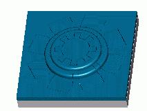
37 Finished micromotor

38 Micromotor after release Cronos MUMPs (formerly MCNC MUMPs)
39 How much should we know about u-fab?

40 Visualize device from a verbal description of the process Being able to draw the process flow diagrams from a description. Shallow pits were etched into n-type substrates, and p-type deflection electrodes were diffused in the above pits, followed by fusion bonding of a second wafer above the first. The top wafer was then ground and polished down to a thickness of 6 um. A passivation layer was then formed on the top wafer and sensing piezoesistors were formed using ion implantation, after which contact holes for metallization to connect to he diffused deflection electrodes were etched. Bond pads and interconnect metallization were then deposited and patterned, followed by etching of the diaphragm from the back of the wafer. Finally, two slots were etched next to the beam to release it over the buried cavity. (Petersen et al., 1991) See
41 Visualize the process steps from a device cross section Visualizing a process from a cross-section. How was this made? See
 Now, owned and operated by Uniphase.")
42 MEMS Foundries You don t have to make them if you don t want to or can t. Cronos MUMPs (formerly MCNC s MUMPs) Now, owned and operated by Uniphase.

")
43 Making elements of mechanisms A surface micromachined hinge (Kris Pister, Berkeley) Substrate hinge


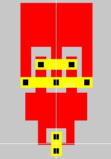
44 Floating hinges Mask layout
45 Electrostatic comb drive Misaligned comb capacitors align creating actuation. Folded-beam suspension Moving combs Shuttle mass anchor Fixed combs

46 Sandia s micro mechanical lock Pin in a maze

47 Close-up of Sandia s micro lock

48 Merry go-around for mites See Sandia s web site for animation
49 Sandia s SUMMiT process revolute joint Rotor Pin Substrate
50 Deep etching Deep RIE (reactive ion etching) to get vertical sidewalls over large depths of several hundred microns. E.g., SCREAM (Cornell) bulk-micromachining
51 SCREAM process Noel MacDonald, Cornell university Deposit and pattern mask oxide Etch bottom sidewall oxide Deep RIE silicon etch Second deep RIE silicon etch Deposit sidewall oxide Isotropic silicon etch
52 Packaging! Packaging access to and protection from the external macro world Packaging is a big problem with MEMS. Sometimes, it may be better not integrate sensor/actuator and electronics. Packaging serves Signal redistribution Mechanical support Power distribution Thermal management Fluidic fittings Etc. Some techniques Ball and wire bonding Flip-chip Sandia s process Research continues
53 Outline What are they? How small are they? How are they useful How do they work? What are they made of? How are they made? How do you design them? What are the modeling and design issues and challenges for us?
54 Modeling and design of MEMS What is different? Integration of sensor, actuator, mechanism, processor, power, and communication makes system level tasks challenging -- common representation for multiple energy domains Device level too has multiple energy domains -- macromodels Component level -- coupled energy domain equations Mask level -- geometric modeling
55 Modeling and design of MEMS System Representing as block diagrams of multi-domain subsystems Device Reduced order macro models of the components Component (physical) Multiple, coupled energy behavioral simulations Artwork of masks and process Defining mask geometry for the process steps Each level involves design There is analysis (forward) problem and synthesis (inverse) problem.
56 The future of MEMS? The proverb: Forecasting is difficult, especially the future. (from Chinese fortune cookies) In any case, MEMS will impact the following industries: Automotive Aerospace Biomedical/bio-tech Health-care Telecommunication Information technology
57 Books Further reading Principles of microfabrication Marc Madou Micromachined transducers: A source book Greg Kovacs Microsystem Design Steve Senturia MEMS: Advanced materials and fabrication methods National Research Council (NRC) committee report, 1997 An Introduction to Microelectromechanical Systems Engineering N. Maluf Microsensors J. W. Gardner Sensor Technology and Devices L. Ristic Transducers, Sensors, and Detectors R. G. Seippel Microactuators: Electrical, Magnetic, Thermal, Optical, Mechanical, Chemical, and Smart Structures M. Tabib-Azar Nano- and Microelectromechanical Systems: Fundamentals of Nano- and Microengineering S. E. Lyshevski
Fabrication Technology, Part II
 EEL5225: Principles of MEMS Transducers (Fall 2003) Fabrication Technology, Part II Agenda: Process Examples TI Micromirror fabrication process SCREAM CMOS-MEMS processes Wafer Bonding LIGA Reading: Senturia,
Dr. Lynn Fuller Webpage:
 ROCHESTER INSTITUTE OF TECHNOLOGY MICROELECTRONIC ENGINEERING Microelectromechanical Systems (MEMs) Process Integration Dr. Lynn Fuller Webpage: http://people.rit.edu/lffeee 82 Lomb Memorial Drive Rochester,
Preface Preface to First Edition
 Contents Foreword Preface Preface to First Edition xiii xv xix CHAPTER 1 MEMS: A Technology from Lilliput 1 The Promise of Technology 1 What Are MEMS or MST? 2 What Is Micromachining? 3 Applications and
Micro and Smart Systems
 Micro and Smart Systems 1. G.K. Ananthasuresh, Mechanical Engineering,IISc IIScsuresh@mecheng.iisc.ernet.in 2. K.J. Vinoy, Electrical Communications Engineering, IISc, kjvinoy@ece.iisc.ernet.in 3. S. Gopalakrishnan,
Micromachining: What you really need to know
 Micromachining: What you really need to know Presented to Proficience #33 class in Jan.-May term of 2005 Lecture 2 G. K. Ananthasuresh suresh@mecheng.iisc.ernet.in Mechanical Engineering Indian Institute
General Introduction to Microstructure Technology p. 1 What is Microstructure Technology? p. 1 From Microstructure Technology to Microsystems
 General Introduction to Microstructure Technology p. 1 What is Microstructure Technology? p. 1 From Microstructure Technology to Microsystems Technology p. 9 The Parallels to Microelectronics p. 15 The
Welcome MNT Conference 1 Albuquerque, NM - May 2010
 Welcome MNT Conference 1 Albuquerque, NM - May 2010 Introduction to Design Outline What is MEMs Design General Considerations Application Packaging Process Flow What s available Sandia SUMMiT Overview
Lecture 10: MultiUser MEMS Process (MUMPS)
") MEMS: Fabrication Lecture 10: MultiUser MEMS Process (MUMPS) Prasanna S. Gandhi Assistant Professor, Department of Mechanical Engineering, Indian Institute of Technology, Bombay, 1 Recap Various VLSI based
MEMS: Fabrication Lecture 10: MultiUser MEMS Process (MUMPS) Prasanna S. Gandhi Assistant Professor, Department of Mechanical Engineering, Indian Institute of Technology, Bombay, 1 Recap Various VLSI based
Evolution of MEMS Technology
 Evolution of MEMS Technology 1 Raksha Sahadev Hukkeri, 2 Shreya Madapurmath, 3 Shreelekha Navale 1,2,3 UG Student, Department of ECE, SDMCET Dharwad Abstract Micro-Electro-Mechanical Systems (MEMS) is
EE C245 ME C218 Introduction to MEMS Design
 EE C245 ME C218 Introduction to MEMS Design Fall 2007 Prof. Clark T.-C. Nguyen Dept. of Electrical Engineering & Computer Sciences University of California at Berkeley Berkeley, CA 94720 Lecture 10: Surface
Today s Class. Materials for MEMS
 Lecture 2: VLSI-based Fabrication for MEMS: Fundamentals Prasanna S. Gandhi Assistant Professor, Department of Mechanical Engineering, Indian Institute of Technology, Bombay, Recap: Last Class What is
4/10/2012. Introduction to Microfabrication. Fabrication
 Introduction to Microfabrication Fabrication 1 MEMS Fabrication Flow Basic Process Flow in Micromachining Nadim Maluf, An introduction to Microelectromechanical Systems Engineering 2 Thin Film Deposition
MEMS II: January 23. Lab 1: Pop-up mirror - PolyMUMPS - Thermal actuators - Mirror CoventorWare
 MEMS II: January 23 Lab 1: Pop-up mirror - PolyMUMPS - Thermal actuators - Mirror CoventorWare Microelectromechanical Systems (MEMS) Multi-User MEMS Processes (MUMPS) Example Design Anchor hole 2.0 0.5
Surface micromachining and Process flow part 1
 Surface micromachining and Process flow part 1 Identify the basic steps of a generic surface micromachining process Identify the critical requirements needed to create a MEMS using surface micromachining
Micro-Scale Engineering I Microelectromechanical Systems (MEMS) Y. C. Lee
 Y. C. Lee") Micro-Scale Engineering I Microelectromechanical Systems (MEMS) Y. C. Lee Department of Mechanical Engineering University of Colorado Boulder, CO 80309-0427 leeyc@colorado.edu September 2, 2008 1 Three
Micro-Scale Engineering I Microelectromechanical Systems (MEMS) Y. C. Lee Department of Mechanical Engineering University of Colorado Boulder, CO 80309-0427 leeyc@colorado.edu September 2, 2008 1 Three
EECS130 Integrated Circuit Devices
 EECS130 Integrated Circuit Devices Professor Ali Javey 9/13/2007 Fabrication Technology Lecture 1 Silicon Device Fabrication Technology Over 10 15 transistors (or 100,000 for every person in the world)
EE C245 ME C218 Introduction to MEMS Design Fall 2007
 EE C245 ME C218 Introduction to MEMS Design Fall 2007 Prof. Clark T.-C. Nguyen Dept. of Electrical Engineering & Computer Sciences University of California at Berkeley Berkeley, CA 94720 Lecture 10: Bulk
Gaetano L Episcopo. Introduction to MEMS
 Gaetano L Episcopo Introduction to MEMS What are MEMS? Micro Electro Mechanichal Systems MEMS are integrated devices, or systems of devices, with microscopic parts, such as: Mechanical Parts Electrical
EE C245 ME C218 Introduction to MEMS Design Fall 2011
 Lecture Outline EE C245 ME C218 Introduction to MEMS Design Fall 2011 Prof. Clark T.-C. Nguyen Dept. of Electrical Engineering & Computer Sciences University of California at Berkeley Berkeley, CA 94720
Cambridge University Press A Guide to Hands-on MEMS Design and Prototyping Joel A. Kubby Excerpt More information.
 1 Introduction 1.1 Overview of MEMS fabrication Microelectromechanical systems (MEMS) fabrication developed out of the thin-film processes first used for semiconductor fabrication. To understand the unique
Lecture 7 CMOS MEMS. CMOS MEMS Processes. CMOS MEMS Processes. Why CMOS-MEMS? Agenda: CMOS MEMS: Fabrication. MEMS structures can be made
 EEL6935 Advanced MEMS (Spring 2005) Instructor: Dr. Huikai Xie CMOS MEMS Agenda: Lecture 7 CMOS MEMS: Fabrication Pre-CMOS Intra-CMOS Post-CMOS Deposition Etching Why CMOS-MEMS? Smart on-chip CMOS circuitry
Regents of the University of California
 Topography Issues Degradation of lithographic resolution PR step coverage, streaking Thickness differences pose problems for reduction steppers Direction of Spin PR PR PR Stringers Problematic when using
Manufacturing Technologies for MEMS and SMART SENSORS
 4 Manufacturing Technologies for MEMS and SMART SENSORS Dr. H. K. Verma Distinguished Professor (EEE) Sharda University, Greater Noida (Formerly: Deputy Director and Professor of Instrumentation Indian
Microsystem Technology: A Survey of the State of the Art
 Microsystem Technology: A Survey of the State of the Art Stephanus BÜTTGENBACH Institute for Microtechnology, Technical University of Braunschweig Langer Kamp 8, D-38106 Braunschweig, Germany Abstract.
Regents of the University of California 1
 Electroplating: Metal MEMS Nickel Surface-Micromachining Process Flow Photoresist Wafer Release Etchant Use electroplating to obtain metal μstructures When thick: call it LIGA Pros: fast low temp deposition,
Tutorial on Micro Electro Mechanical Systems (MEMS)
") Tutorial on Micro Electro Mechanical Systems (MEMS) Bruce Kim Department of Electrical, 1 ! What is MEMS! Why MEMS! Applications! MEMS Fabrication! MEMS Packaging! Conclusion MEMS 2 WHAT IS MEMS! MEMS
Tutorial on Micro Electro Mechanical Systems (MEMS) Bruce Kim Department of Electrical, 1 ! What is MEMS! Why MEMS! Applications! MEMS Fabrication! MEMS Packaging! Conclusion MEMS 2 WHAT IS MEMS! MEMS
Mikrosensorer. Microfabrication 1
 Mikrosensorer Microfabrication 1 Literature Introductory MEMS Fabrication and Applications Thomas M. Adams and Richard A. Layton Available as ebook on http://www.lub.lu.se/en/search/lubsearch.html This
Chapter 2 OVERVIEW OF MEMS
 6 Chapter 2 OVERVIEW OF MEMS 2.1 MEMS and Microsystems The term MEMS is an abbreviation of microelectromechanical system. MEMS contains components ofsizes in 1 micrometer to 1 millimeter. The core element
Lecture 3: Integrated Processes
 Lecture 3: Integrated Processes Single-Crystal Silicon Process Integration Polysilicon Micromachining Process Integrated CMOS Micromachining Process ENE 5400, Spring 2004 1 Single Crystal Silicon ENE 5400,
Thomas M. Adams Richard A. Layton. Introductory MEMS. Fabrication and Applications. Springer
 Thomas M. Adams Richard A. Layton Introductory MEMS Fabrication and Applications Springer Contents Preface xiü Part I Fabrication Chapter 1: Introduction 3 1.1 What are MEMS? 3 1.2 Why MEMS? 4 1.2.1. Low
Surface Micromachining II
 Surface Micromachining II Dr. Thara Srinivasan Lecture 4 Picture credit: Sandia National Lab Lecture Outline Reading From reader: Bustillo, J. et al., Surface Micromachining of Microelectromechanical Systems,
Chapter 3 Silicon Device Fabrication Technology
 Chapter 3 Silicon Device Fabrication Technology Over 10 15 transistors (or 100,000 for every person in the world) are manufactured every year. VLSI (Very Large Scale Integration) ULSI (Ultra Large Scale
Introduction to Microeletromechanical Systems (MEMS) Lecture 5 Topics. JDS Uniphase MUMPs
 Lecture 5 Topics. JDS Uniphase MUMPs") Introduction to Microeletromechanical Systems (MEMS) Lecture 5 Topics JDS Uniphase MUMPS Foundry Process and Devices Foundry Process Sequence Design Rules and Process Interactions Examples CMOS for MEMS
Introduction to Microeletromechanical Systems (MEMS) Lecture 5 Topics JDS Uniphase MUMPS Foundry Process and Devices Foundry Process Sequence Design Rules and Process Interactions Examples CMOS for MEMS
Single crystal silicon supported thin film micromirrors for optical applications
 Single crystal silicon supported thin film micromirrors for optical applications Zhimin J. Yao* Noel C. MacDonald Cornell University School of Electrical Engineering and Cornell Nanofabrication Facility
CMOS Technology. Flow varies with process types & company. Start with substrate selection. N-Well CMOS Twin-Well CMOS STI
 CMOS Technology Flow varies with process types & company N-Well CMOS Twin-Well CMOS STI Start with substrate selection Type: n or p Doping level, resistivity Orientation, 100, or 101, etc Other parameters
MEMSAND MICROSYSTEMS Design, Manufacture, and Nanoscale Engineering
 MEMSAND MICROSYSTEMS Design, Manufacture, and Nanoscale Engineering Second Edition TAI-RAN HSU Microsystems Design and Packaging Laboratory Department of Mechanical and Aerospace Engineering San Jose State
MEMS Fabrication. Beyond Integrated Circuits. MEMS Basic Concepts
 MEMS Fabrication Beyond Integrated Circuits MEMS Basic Concepts Uses integrated circuit fabrication techniques to make mechanical as well as electrical components on a single chip. Small size 1µm 1mm Typically
Poly-SiGe MEMS actuators for adaptive optics
 Poly-SiGe MEMS actuators for adaptive optics Blake C.-Y. Lin a,b, Tsu-Jae King a, and Richard S. Muller a,b a Department of Electrical Engineering and Computer Sciences, b Berkeley Sensor and Actuator
Ultrasonic Micromachining in the fabrication of MEMS Micro-sensors
 Ultrasonic Micromachining in the fabrication of MEMS Micro-sensors Jamil Akhtar Professor AcSIR New Delhi Chief Scientist & Head, CSIR-CEERI, Pilani, INDIA CEERI, Pilani A constituent laboratory of CSIR,
Applications of High-Performance MEMS Pressure Sensors Based on Dissolved Wafer Process
 Applications of High-Performance MEMS Pressure Sensors Based on Dissolved Wafer Process Srinivas Tadigadapa and Sonbol Massoud-Ansari Integrated Sensing Systems (ISSYS) Inc., 387 Airport Industrial Drive,
EE 330 Lecture 9. IC Fabrication Technology Part 2
 EE 330 Lecture 9 IC Fabrication Technology Part 2 Quiz 8 A 2m silicon crystal is cut into wafers using a wire saw. If the wire diameter is 220um and the wafer thickness is 350um, how many wafers will this
Materials for MEMS. Dr. Yael Hanein. 11 March 2004 Materials Applications Yael Hanein
 Materials for MEMS Dr. Yael Hanein Materials for MEMS MEMS (introduction) Materials used in MEMS Material properties Standard MEMS processes MEMS The world s smallest guitar is about 10 micrometers long
MEMS Devices. Fraunhofer Institute for Silicon Technology ISIT. Itzehoe, Germa. any
 Examples of CMP Processess for the Manufacturing of MEMS Devices Gerfried Zwicke er Fraunhofer Institute for Silicon Technology ISIT Itzehoe, Germa any gerfried.zwicker@isit.fraunhofer.de Contents MEMS
PROCESS FLOW AN INSIGHT INTO CMOS FABRICATION PROCESS
 Contents: VI Sem ECE 06EC63: Analog and Mixed Mode VLSI Design PROCESS FLOW AN INSIGHT INTO CMOS FABRICATION PROCESS 1. Introduction 2. CMOS Fabrication 3. Simplified View of Fabrication Process 3.1 Alternative
4. Process Integration: Case Studies
 Case Study #2: FCantilevered Microgripper Surface Machined MEMS Case Study #2: FCantilevered Microgripper Sandia Lucent Sandia Integrated Accelerometers Optomechanical Systems Integrated Sensors 1 Bulk
EE 5344 Introduction to MEMS. CHAPTER 3 Conventional Si Processing
 3. Conventional licon Processing Micromachining, Microfabrication. EE 5344 Introduction to MEMS CHAPTER 3 Conventional Processing Why silicon? Abundant, cheap, easy to process. licon planar Integrated
Course Code: BMEG5100 Course Title: Advanced Medical Robotics Course Code: BMEG5110 Course Title: Advanced Medical Devices and Sensor Networks
 Course Code: BMEG5100 Course Title: Advanced Medical Robotics Review of medical robotics fundamentals; introduction to robotics enabled endoscopic and laparoscopic surgeries; concepts of robotics based
The Physical Structure (NMOS)
") The Physical Structure (NMOS) Al SiO2 Field Oxide Gate oxide S n+ Polysilicon Gate Al SiO2 SiO2 D n+ L channel P Substrate Field Oxide contact Metal (S) n+ (G) L W n+ (D) Poly 1 3D Perspective 2 3 Fabrication
The Physical Structure (NMOS) Al SiO2 Field Oxide Gate oxide S n+ Polysilicon Gate Al SiO2 SiO2 D n+ L channel P Substrate Field Oxide contact Metal (S) n+ (G) L W n+ (D) Poly 1 3D Perspective 2 3 Fabrication
EE40 Lec 22. IC Fabrication Technology. Prof. Nathan Cheung 11/19/2009
 Suggested Reading EE40 Lec 22 IC Fabrication Technology Prof. Nathan Cheung 11/19/2009 300mm Fab Tour http://www-03.ibm.com/technology/manufacturing/technology_tour_300mm_foundry.html Overview of IC Technology
Optical MEMS in Communication and Sensing. Micromirror Arrays
 Optical MEMS in Communication and Sensing Fabrication, Design, and Scaling of Optical Microsystems Olav Solgaard University Introduction to Optical MEMS Opportunities and challenges Fabrication MEMS fabrication
FABRICATION PROCESSES FOR MAGNETIC MICROACTUATORS WITH POLYSILICON FLEXURES. Jack W. Judy and Richard S. Muller
 FABRICATION PROCESSES FOR MAGNETIC MICROACTUATORS WITH POLYSILICON FLEXURES Jack W. Judy and Richard S. Muller Berkeley Sensor & Actuator Center (BSAC) Department of EECS, University of California, Berkeley,
Sensor. Device that converts a non-electrical physical or chemical quantity into an electrical signal. Sensor Processor Display Output signal
 Microsensors Outline Sensor & microsensor Force and pressure microsensors Position and speed microsensors Acceleration microsensors Chemical microsensors Biosensors Temperature sensors Sensor Device that
Micromachining AMT 2505
 Micromachining AMT 2505 Shanmuga Raja.B (BVB0912004) Module leader : Mr. Raja Hussain Introduction Micromachining are inherently connected to the evolution of Micro Electro Mechanical Systems (MEMS). Decades
GE Sensing & Inspection Technologies MEMS. Global Solutions for Microsystems
 GE Sensing & Inspection Technologies MEMS Global Solutions for Microsystems g Global research, development and manufacturing excellence Groby, United Kingdom MEMS Design and Manufacturing Center Advanced
PETER PAZMANY CATHOLIC UNIVERSITY Consortium members SEMMELWEIS UNIVERSITY, DIALOG CAMPUS PUBLISHER
 PETER PAZMANY CATHOLIC UNIVERSITY SEMMELWEIS UNIVERSITY Development of Complex Curricula for Molecular Bionics and Infobionics Programs within a consortial* framework** Consortium leader PETER PAZMANY
EE 330 Lecture 9. IC Fabrication Technology Part II. -Oxidation -Epitaxy -Polysilicon -Planarization -Resistance and Capacitance in Interconnects
 EE 330 Lecture 9 IC Fabrication Technology Part II -Oxidation -Epitaxy -Polysilicon -Planarization -Resistance and Capacitance in Interconnects Review from Last Time IC Fabrication Technology Crystal Preparation
Fabrication Process. Crystal Growth Doping Deposition Patterning Lithography Oxidation Ion Implementation CONCORDIA VLSI DESIGN LAB
 Fabrication Process Crystal Growth Doping Deposition Patterning Lithography Oxidation Ion Implementation 1 Fabrication- CMOS Process Starting Material Preparation 1. Produce Metallurgical Grade Silicon
Lecture 5. SOI Micromachining. SOI MUMPs. SOI Micromachining. Silicon-on-Insulator Microstructures. Agenda:
 EEL6935 Advanced MEMS (Spring 2005) Instructor: Dr. Huikai Xie SOI Micromachining Agenda: SOI Micromachining SOI MUMPs Multi-level structures Lecture 5 Silicon-on-Insulator Microstructures Single-crystal
PHYS 534 (Fall 2008) Process Integration OUTLINE. Examples of PROCESS FLOW SEQUENCES. >Surface-Micromachined Beam
 Process Integration OUTLINE. Examples of PROCESS FLOW SEQUENCES. >Surface-Micromachined Beam") PHYS 534 (Fall 2008) Process Integration Srikar Vengallatore, McGill University 1 OUTLINE Examples of PROCESS FLOW SEQUENCES >Semiconductor diode >Surface-Micromachined Beam Critical Issues in Process
PHYS 534 (Fall 2008) Process Integration Srikar Vengallatore, McGill University 1 OUTLINE Examples of PROCESS FLOW SEQUENCES >Semiconductor diode >Surface-Micromachined Beam Critical Issues in Process
Tackling the optical interconnection challenge for the Integrated Photonics Revolution
 Tackling the optical interconnection challenge for the Integrated Photonics Revolution Dr. Ir. TU Delft, Precision and Microsystems Engineering m.tichem@tudelft.nl Microfabrication and MEMS Si microfabrication
Complexity of IC Metallization. Early 21 st Century IC Technology
 EECS 42 Introduction to Digital Electronics Lecture # 25 Microfabrication Handout of This Lecture. Today: how are Integrated Circuits made? Silicon wafers Oxide formation by growth or deposition Other
EE 330 Lecture 8. IC Fabrication Technology Part II. - Oxidation - Epitaxy - Polysilicon - Interconnects
 EE 330 Lecture 8 IC Fabrication Technology Part II - Oxidation - Epitaxy - Polysilicon - Interconnects Review from Last Time MOS Transistor Bulk Source Gate Drain p-channel MOSFET Lightly-doped n-type
Surface Micromachining and Inertial Sensors
 Surface Micromachining and Inertial Sensors Tutorial 2A Bob Sulouff Analog Devices Inc. Cambridge, MA. 02139 Bob.Sulouff@Analog.com 617-761- Presentation Outline Technology of MEMS Surface Micromachined
applied to Biomedical Instrumentation Microfabrication and Nanofabrication Microtechnology Nanotechnology Biomedical Lecture 9 and
 Lecture 9 Biomedical Microtechnology and Nanotechnology Microfabrication and Nanofabrication applied to Biomedical Instrumentation Why Micro/Nano? SCALING OF PARAMETERS The values of various parameters
MATERIALS AND RELIABILITY ISSUES IN MEMS AND MICROSYSTEMS
 MATERIALS AND RELIABILITY ISSUES IN MEMS AND MICROSYSTEMS By Aris Christou Materials Science and Engineering University of Maryland College Park, MD 20742-2115 Introduction To Microelectromechanical Systems
Microfabrication of Heterogeneous, Optimized Compliant Mechanisms SUNFEST 2001 Luo Chen Advisor: Professor G.K. Ananthasuresh
 Microfabrication of Heterogeneous, Optimized Compliant Mechanisms SUNFEST 2001 Luo Chen Advisor: Professor G.K. Ananthasuresh Fig. 1. Single-material Heatuator with selective doping on one arm (G.K. Ananthasuresh)
PRESSURE SENSOR MODEL ACTIVITY. Pressure Sensor Model Activity
 PRESSURE SENSOR MODEL ACTIVITY Pressure Sensor Model Activity Unit Overview This activity uses household materials to build a pressure sensor Wheatstone Bridge sensing circuit Flexible diaphragm Reference
Supporting Information: Model Based Design of a Microfluidic. Mixer Driven by Induced Charge Electroosmosis
 Supporting Information: Model Based Design of a Microfluidic Mixer Driven by Induced Charge Electroosmosis Cindy K. Harnett, Yehya M. Senousy, Katherine A. Dunphy-Guzman #, Jeremy Templeton * and Michael
Research Projects in Microelectromechanical Systems (MEMS) and Microfluidics
 and Microfluidics") Research Projects in Microelectromechanical Systems (MEMS) and Microfluidics Luc G. Fréchette, Ph.D. Associate Professor Canada Research Chair in Microfluidics and Power MEMS Department of Mechanical Engineering
Research Projects in Microelectromechanical Systems (MEMS) and Microfluidics Luc G. Fréchette, Ph.D. Associate Professor Canada Research Chair in Microfluidics and Power MEMS Department of Mechanical Engineering
6.777J/2.732J Design and Fabrication of Microelectromechanical Devices Spring Term Solution to Problem Set 2 (16 pts)
") 6.777J/2.732J Design and Fabrication of Microelectromechanical Devices Spring Term 2007 By Brian Taff (Adapted from work by Feras Eid) Solution to Problem Set 2 (16 pts) Issued: Lecture 4 Due: Lecture
6.777J/2.732J Design and Fabrication of Microelectromechanical Devices Spring Term 2007 By Brian Taff (Adapted from work by Feras Eid) Solution to Problem Set 2 (16 pts) Issued: Lecture 4 Due: Lecture
KGC SCIENTIFIC Making of a Chip
 KGC SCIENTIFIC www.kgcscientific.com Making of a Chip FROM THE SAND TO THE PACKAGE, A DIAGRAM TO UNDERSTAND HOW CPU IS MADE? Sand CPU CHAIN ANALYSIS OF SEMICONDUCTOR Material for manufacturing process
ASIM-X MEMS-Specific Design Rules
 ASIM-X MEMS-Specific Design Rules Version 2 Revised April 5, 2006. This is a beta version, subject to change. Revised by G. K. Fedder, Carnegie Mellon University. 1 Process Overview ASIM-X, an acronym
Shock Testing of MEMS Devices
 Shock Testing of MEMS Devices Michelle A. Duesterhaus Vesta I. Bateman Darren A. Hoke Sandia National Laboratories, P.O. Box 5800 MS-1310, Albuquerque, NM 87185-1310 ABSTRACT Micro-Electro-Mechanical Systems
INF5490 RF MEMS. LN02: MEMS Fabrication. Spring 2012, Oddvar Søråsen Department of Informatics, UoO
 INF5490 RF MEMS LN02: MEMS Fabrication Spring 2012, Oddvar Søråsen Department of Informatics, UoO 1 Micromachining Today s lecture Important process steps General Summary: MEMS-specific steps Examples
Surface Micromachining
 Surface Micromachining Micro Actuators, Sensors, Systems Group University of Illinois at Urbana-Champaign Outline Definition of surface micromachining Most common surface micromachining materials - polysilicon
L5: Micromachining processes 1/7 01/22/02
 97.577 L5: Micromachining processes 1/7 01/22/02 5: Micromachining technology Top-down approaches to building large (relative to an atom or even a transistor) structures. 5.1 Bulk Micromachining A bulk
CTN 10/1/09. EE 245: Introduction to MEMS Lecture 11: Bulk Micromachining. Copyright 2009 Regents of the University of California
 MUMPS: MultiUser MEMS ProcesS Foundry MEMS: The MUMPS Process Originally created by the Microelectronics Center of North Carolina (MCNC) now owned by MEMSCAP in France Three-level polysilicon surface micromachining
Mostafa Soliman, Ph.D. May 5 th 2014
 Mostafa Soliman, Ph.D. May 5 th 2014 Mostafa Soliman, Ph.D. 1 Basic MEMS Processes Front-End Processes Back-End Processes 2 Mostafa Soliman, Ph.D. Wafers Deposition Lithography Etch Chips 1- Si Substrate
MEMS and Nanotechnology
 MEMS and Nanotechnology slide 1 table of contents 1. 2. 3. 4. 5. 6. introduction definition of MEMS & NEMS active principles types of MEMS fabrication problems with the fabrication slide 2 progress 1.
Chapter 3 CMOS processing technology
 Chapter 3 CMOS processing technology (How to make a CMOS?) Si + impurity acceptors(p-type) donors (n-type) p-type + n-type => pn junction (I-V) 3.1.1 (Wafer) Wafer = A disk of silicon (0.25 mm - 1 mm thick),
Microelectronics. Integrated circuits. Introduction to the IC technology M.Rencz 11 September, Expected decrease in line width
 Microelectronics Introduction to the IC technology M.Rencz 11 September, 2002 9/16/02 1/37 Integrated circuits Development is controlled by the roadmaps. Self-fulfilling predictions for the tendencies
Silicon Wafer Processing PAKAGING AND TEST
 Silicon Wafer Processing PAKAGING AND TEST Parametrical test using test structures regularly distributed in the wafer Wafer die test marking defective dies dies separation die fixing (not marked as defective)
ELEC 3908, Physical Electronics, Lecture 4. Basic Integrated Circuit Processing
 ELEC 3908, Physical Electronics, Lecture 4 Basic Integrated Circuit Processing Lecture Outline Details of the physical structure of devices will be very important in developing models for electrical behavior
EE C245 ME C218 Introduction to MEMS Design Fall 2007
 EE C245 ME C218 Introduction to MEMS Design Fall 2007 Prof. Clark T.-C. Nguyen Dept. of Electrical Engineering & Computer Sciences University of California at Berkeley Berkeley, CA 94720 Lecture 9: Surface
Lecture 19 Microfabrication 4/1/03 Prof. Andy Neureuther
 EECS 40 Spring 2003 Lecture 19 Microfabrication 4/1/03 Prof. ndy Neureuther How are Integrated Circuits made? Silicon wafers Oxide formation by growth or deposition Other films Pattern transfer by lithography
ME 189 Microsystems Design and Manufacture. Chapter 9. Micromanufacturing
 ME 189 Microsystems Design and Manufacture Chapter 9 Micromanufacturing This chapter will offer an overview of the application of the various fabrication techniques described in Chapter 8 in the manufacturing
Solid State Sensors. Microfabrication 8/22/08 and 8/25/08
 Solid State Sensors Microfabrication 8/22/08 and 8/25/08 Purpose of This Material To introduce the student to microfabrication techniques as used to fabricate MEMS Sensors Understand concepts not specifics
SUMMiT V Five Level Surface Micromachining Technology Design Manual
 SUMMiT V Five Level Surface Micromachining Technology Design Manual Version 1.3 09/22/2005 MEMS Devices and Reliability Physics Department Microelectronics Development Laboratory Sandia National Laboratories
Process Integration. MEMS Release Techniques Sacrificial Layer Removal Substrate Undercut
 Process Integration Self-aligned Techniques LOCOS- self-aligned channel stop Self-aligned Source/Drain Lightly Doped Drain (LDD) Self-aligned silicide (SALICIDE) Self-aligned oxide gap MEMS Release Techniques
FABRICATION OF CMOS INTEGRATED CIRCUITS. Dr. Mohammed M. Farag
 FABRICATION OF CMOS INTEGRATED CIRCUITS Dr. Mohammed M. Farag Outline Overview of CMOS Fabrication Processes The CMOS Fabrication Process Flow Design Rules EE 432 VLSI Modeling and Design 2 CMOS Fabrication
Microfabrication of Integrated Circuits
 Microfabrication of Integrated Circuits OUTLINE History Basic Processes Implant; Oxidation; Photolithography; Masks Layout and Process Flow Device Cross Section Evolution Lecture 38, 12/05/05 Reading This
VLSI. Lecture 1. Jaeyong Chung System-on-Chips (SoC) Laboratory Incheon National University. Based on slides of David Money Harris
 Laboratory Incheon National University. Based on slides of David Money Harris") VLSI Lecture 1 Jaeyong Chung System-on-Chips (SoC) Laboratory Incheon National University Based on slides of David Money Harris Goals of This Course Learn the principles of VLSI design Learn to design
VLSI Lecture 1 Jaeyong Chung System-on-Chips (SoC) Laboratory Incheon National University Based on slides of David Money Harris Goals of This Course Learn the principles of VLSI design Learn to design
Lecture #18 Fabrication OUTLINE
 Transistors on a Chip Lecture #18 Fabrication OUTLINE IC Fabrication Technology Introduction the task at hand Doping Oxidation Thin-film deposition Lithography Etch Lithography trends Plasma processing
Integrated Processes. Lecture Outline
 Integrated Processes Thara Srinivasan Lecture 14 Picture credit: Lemkin et al. Lecture Outline From reader Bustillo, J. et al., Surface micromachining of MEMS, pp. 1556-9. A.E. Franke et al., Polycrystalline
FABRICATION ENGINEERING MICRO- NANOSCALE ATTHE AND. Fourth Edition STEPHEN A. CAMPBELL. of Minnesota. University OXFORD UNIVERSITY PRESS
 AND FABRICATION ENGINEERING ATTHE MICRO- NANOSCALE Fourth Edition STEPHEN A. CAMPBELL University of Minnesota New York Oxford OXFORD UNIVERSITY PRESS CONTENTS Preface xiii prrt i OVERVIEW AND MATERIALS
MICRO-ELECTRO-MECHANICAL VARIABLE BLAZE GRATINGS
 MICRO-ELECTRO-MECHANICAL VARIABLE BLAZE GRATINGS D. M. Burns and V. M. Bright Air Force Institute of Technology Department of Electrical and Computer Engineering Wright-Patterson Air Force Base, OH 45433-7765
Chapter 4 : ULSI Process Integration (0.18 m CMOS Process)
") Chapter : ULSI Process Integration (0.8 m CMOS Process) Reference. Semiconductor Manufacturing Technology : Michael Quirk and Julian Serda (00). - (00). Semiconductor Physics and Devices- Basic Principles(/e)
Chapter : ULSI Process Integration (0.8 m CMOS Process) Reference. Semiconductor Manufacturing Technology : Michael Quirk and Julian Serda (00). - (00). Semiconductor Physics and Devices- Basic Principles(/e)
UT Austin, ECE Department VLSI Design 2. CMOS Fabrication, Layout Rules
 2. CMOS Fabrication, Layout, Design Rules Last module: Introduction to the course How a transistor works CMOS transistors This module: CMOS Fabrication Design Rules CMOS Fabrication CMOS transistors are
Lecture 8-1 MCNC/MUMPS Process
 F. G. Tseng Fall/2016, 8-1, p1 Lecture 8-1 MCNC/MUMPS Process!! MCNC/MUMPS structure Layers provided: 7.0 µm Cr/Au=0.5 poly2=1.5 ox2=0.5 poly1=2.0 ox1=2.0 Poly0=0.5 Nitride=0.5 MUMPS Cross section with